
September 1995
1/53
This is advance information from SGS-THOMSON. Details are subject to change without notice.
ST10R165
16-BIT ROMLESS MICROCONTROLLER
ADVANCE DATA
■
High performance 16-bit CPU with 4-stage
pipeline
■
100 nsinstructioncycle timeat20-MHz CPUclock
■
500 ns multiplication (16
×
16 bits), 1
µ
s division
(32 / 16 bit)
■
Enhanced boolean bit manipulation facilities
■
Additional instructions to support HLL and
operating systems
■
Register-based design with multiple variable
register banks
■
Single-cycle context switching support
■
Up to 16 Mbytes linear address space for code
and data
■
2 Kbytes on-chip RAM
■
Programmable external bus characteristics for
different address ranges
■
8-Bit or 16-bit external data bus
■
Multiplexed or demultiplexed external address/
data buses
■
Five programmable chip-select signals
■
Hold- and hold-acknowledge bus arbitration
support
■
1024 bytes on-Chip special function register area
■
Idle and power down modes
■
8-channel interrupt-driven single-cycle data
transfer facilities via peripheral event controller
(PEC)
■
16-priority-level
interrupt
system
with
28
sources, sample-rate down to 50 ns
■
Two multi-functional general purpose timer
units with 5 timers
■
Two
serial
channels
(synchronous/
asynchronous and high-speed-synchronous)
■
Programmable watchdog timer
■
Up to 77 general purpose I/O lines
■
Supported by a wealth of development tools like
C-compilers,
macro-assembler
packages,
emulators, evaluation boards, HLL-debuggers,
simulators,
logic
analyser
disassemblers,
programming boards
■
On-chip bootstrap loader
■
100-Pin TQFP and PQFP package (EIAJ)
PQFP100
TQFP100
(Ordering Information at the end of the datasheet)

TABLE OF CONTENTS
2/53
ST10R165 . . . . . . . . . . . . . . . . . . . . . . . . . . . . . . . . . . . . . . . 1
1 INTRODUCTION . . . . . . . . . . . . . . . . . . . . . . . . . . . . . . . . . . . . . . . . . . . . . . . 3
2 FUNCTIONAL DESCRIPTION . . . . . . . . . . . . . . . . . . . . . . . . . . . . . . . . . . . 10
3 MEMORY ORGANIZATION . . . . . . . . . . . . . . . . . . . . . . . . . . . . . . . . . . . . . 11
4 EXTERNAL BUS CONTROLLER . . . . . . . . . . . . . . . . . . . . . . . . . . . . . . . . . 12
5 CENTRAL PROCESSING UNIT (CPU) . . . . . . . . . . . . . . . . . . . . . . . . . . . . 13
6 INTERRUPT SYSTEM . . . . . . . . . . . . . . . . . . . . . . . . . . . . . . . . . . . . . . . . . 15
7 GENERAL PURPOSE TIMER (GPT) UNIT . . . . . . . . . . . . . . . . . . . . . . . . . 18
8 PARALLEL PORTS . . . . . . . . . . . . . . . . . . . . . . . . . . . . . . . . . . . . . . . . . . . . 21
9 SERIAL CHANNELS . . . . . . . . . . . . . . . . . . . . . . . . . . . . . . . . . . . . . . . . . . . 21
10 WATCHDOG TIMER . . . . . . . . . . . . . . . . . . . . . . . . . . . . . . . . . . . . . . . . . . 22
11 INSTRUCTION SET SUMMARY . . . . . . . . . . . . . . . . . . . . . . . . . . . . . . . . 23
12 SPECIAL FUNCTION REGISTER OVERVIEW . . . . . . . . . . . . . . . . . . . . . 25
13 ELECTRICAL CHARACTERISTICS . . . . . . . . . . . . . . . . . . . . . . . . . . . . . . 29
13.1
ABSOLUTE MAXIMUM RATINGS . . . . . . . . . . . . . . . . . . . . . . . . . . 29
13.2
PARAMETER INTERPRETATION . . . . . . . . . . . . . . . . . . . . . . . . . . 29
13.3
DC CHARACTERISTICS . . . . . . . . . . . . . . . . . . . . . . . . . . . . . . . . . 30
13.4
TESTING WAVEFORMS . . . . . . . . . . . . . . . . . . . . . . . . . . . . . . . . . 33
13.5
AC CHARACTERISTICS . . . . . . . . . . . . . . . . . . . . . . . . . . . . . . . . . 34
14 PACKAGE MECHANICAL DATA . . . . . . . . . . . . . . . . . . . . . . . . . . . . . . . . 52
15 ORDERING INFORMATION . . . . . . . . . . . . . . . . . . . . . . . . . . . . . . . . . . . . 53
ST10R165
3/53
1 INTRODUCTION
The ST10R165 is a new derivative of the SGS
-
THOMSON ST10 family of full fea-
tured single-chip CMOS microcontrollers. It combines high CPU performance (up to
10 million instructions per second) with high peripheral functionality and enhanced
IO-capabilities.
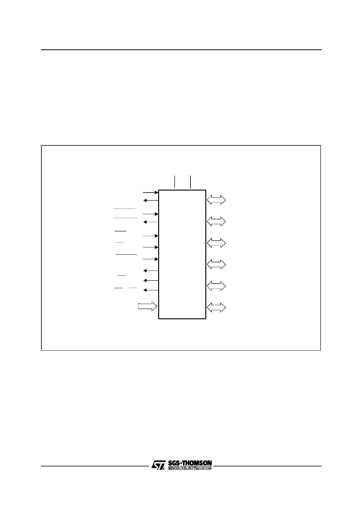
Figure 1. Logic Symbol
Port 6
8-Bit
Port 5
6-Bit
Port 4
8-Bit
Port 3
15-Bit
Port 2
8-Bit
Port 1
16-Bit
Port 0
16-Bit
V
DD
Vss
XTAL 2
XTAL 1
ALE
WR/WRL
RST in
RST out
NMI
EA
RD
READY
VR02045D
ST10R165
4/53
ST10R165
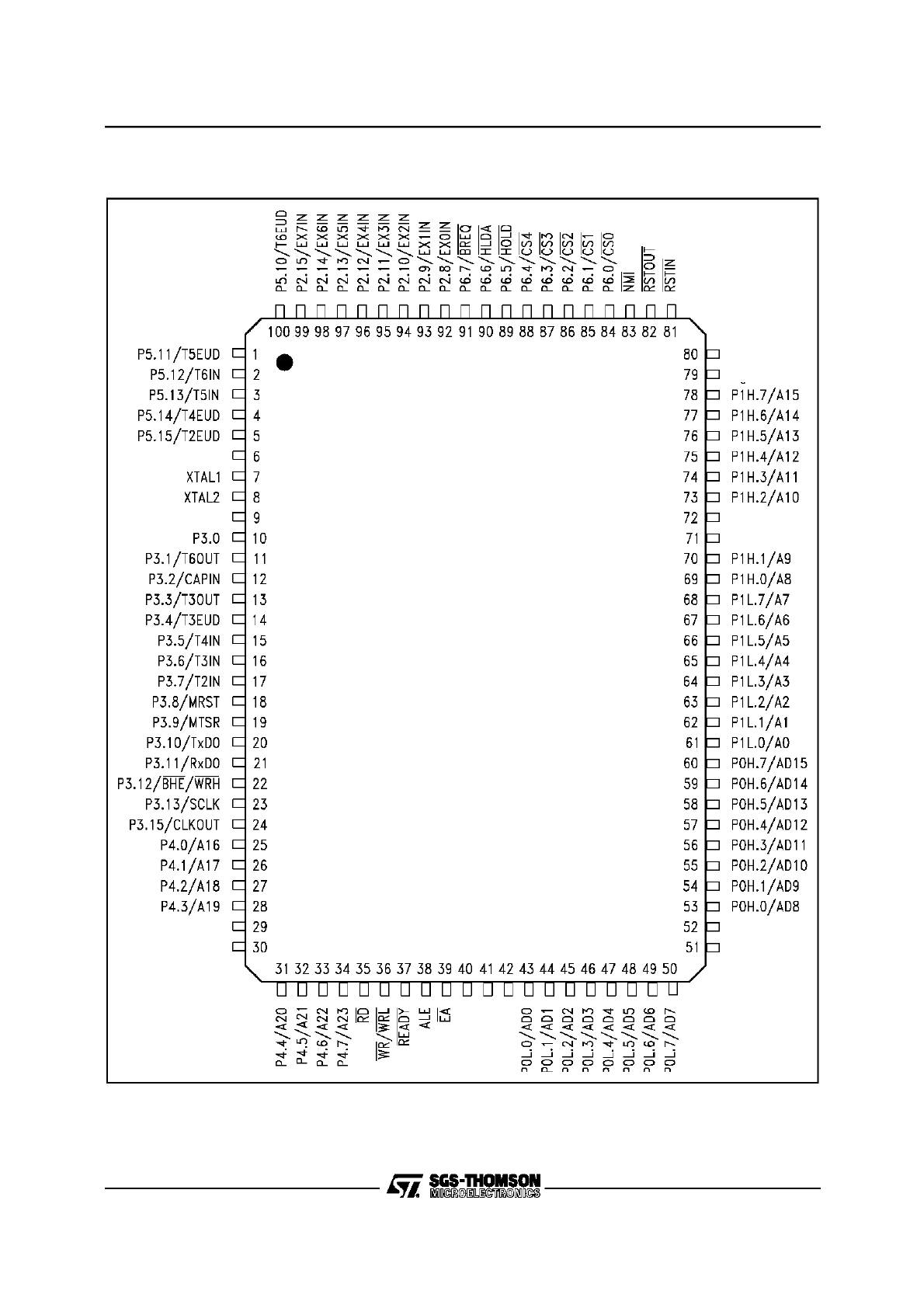
Figure 2. PQFP Pin Configuration (top view)
V
DD
V
SS
V
PP
V
DD
V
DD
V
DD
V
SS
V
SS
V
SS
V
DD
V
DD
V
SS
V
SS
ST10R165
VR02052B
ST10R165
5/53
Figure 3. TQFP Pin Configuration (top view)
ST10R165
VR02052A
1
2
3
4
5
7
6
9
8
10
11
12
13
14
16
15
18
17
19
20
21
22
23
25
24
P5.13/T5in
P5.14/T4EUD
P5.15/T2EUD
XTAL1
XTAL2
P3.0
P3.1/T6OUT
P3.2/CAPIN
P3.3/T3OUT
P3.4/T3EUD
P3.5/T4IN
P3.6/T3IN
P3.7/T2IN
P3.8/MRST
P3.9/MTSR
P3.10/TxD0
P3.11/RxD0
P3.13/SCLK
P3.15/CLKOUT
P4.0/A16
P4.1/A17
P4.2/A18
P3.12/BHE/WRH
75
74
73
72
71
69
70
67
68
66
65
64
63
62
60
61
58
59
57
56
55
54
53
51
52
26
28
27
30
29
32
31
34 35
33
37
36
40
39
38
43
42
41
46
45
44
48
47
50
49
100
98
99
96
97
94
95
92 91
93
89
90
86
87
88
83
84
85
80
81
82
78
79
76
77
P1L.0/A0
P1H.6/A14
P1H.5/A13
P1H.4/A12
P1H.3/A11
P1H.2/A10
P1H.0/A8
P1L.7/A7
P1L.6/A6
P1L.5/A5
P1H.1/A9
P1L.3/A3
P1L.2/A2
P1L.1/A1
P1L.4/A4
P0H.7/AD15
P0H.6/AD14
P0H.5/AD13
P0H.4/AD12
P0H.3/AD11
P0H.2/AD10
P0H.1/AD9
P0H.0/AD8
P4
.4
/A2
0
P
4
.3
/A
1
9
P4
.5/
A
2
1
P4
.6
/A
2
2
P4
.7
/A
2
3
P0
L
.0
/A
D
0
P
0
L.
1/
A
D
1
P
0
L.
2/
A
D
2
P
0
L.
3/
A
D
3
P
0
L.
4/
A
D
4
P
0
L.
5/
A
D
5
P
0
L.
6/
A
D
6
P
0
L.
7/
A
D
7
AL
E
RD
P1
H
.7
/A1
5
NM
I
P
5
.1
2
/T
6
IN
P2
.14
/EX6
IN
P2
.13
/EX5
IN
P2
.12
/EX4
IN
P5
.1
1
/T
5
EU
D
P5
.1
0
/T
6
E
U
D
P2
.15
/EX7
IN
P2
.11
/EX3
IN
P2
.10
/EX2
IN
P2
.9/
EX1
IN
P2
.8/
EX0
IN
V
DD
V
SS
V
DD
V
SS
V
DD
V
SS
P6
.7/
B
R
E
Q
P6
.6/
H
LDA
P6
.5/
H
O
L
D
P6
.4/
C
S4
P6
.3/
C
S3
P6
.2/
C
S2
P6
.1/
C
S1
P6
.0/
C
S0
RS
T
IN
RS
T
O
UT
V
SS
V
PP
V
DD
V
DD
V
SS
V
DD
V
SS
WR
/W
R
L
RE
A
D
Y
EA
6/53
ST10R165
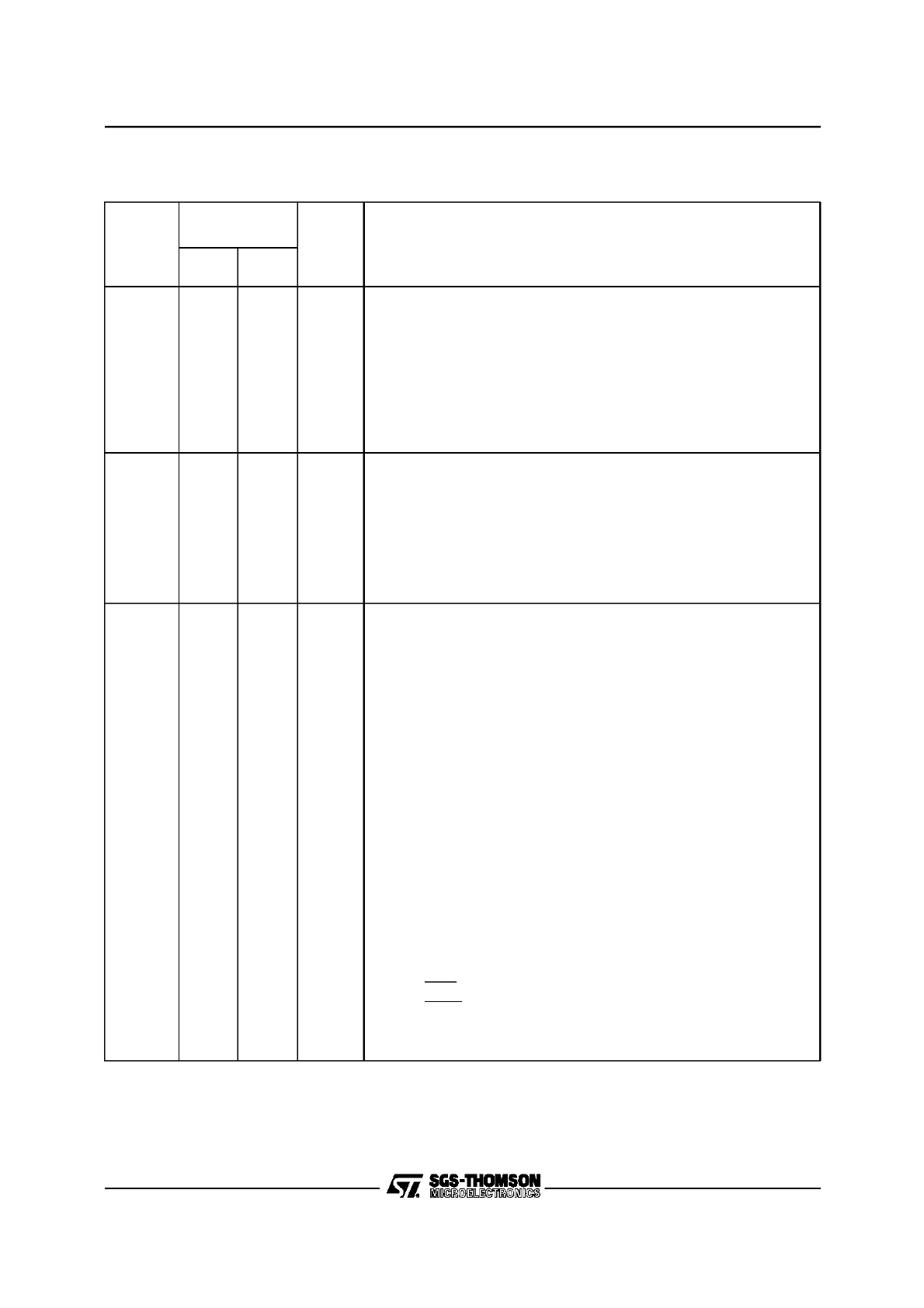
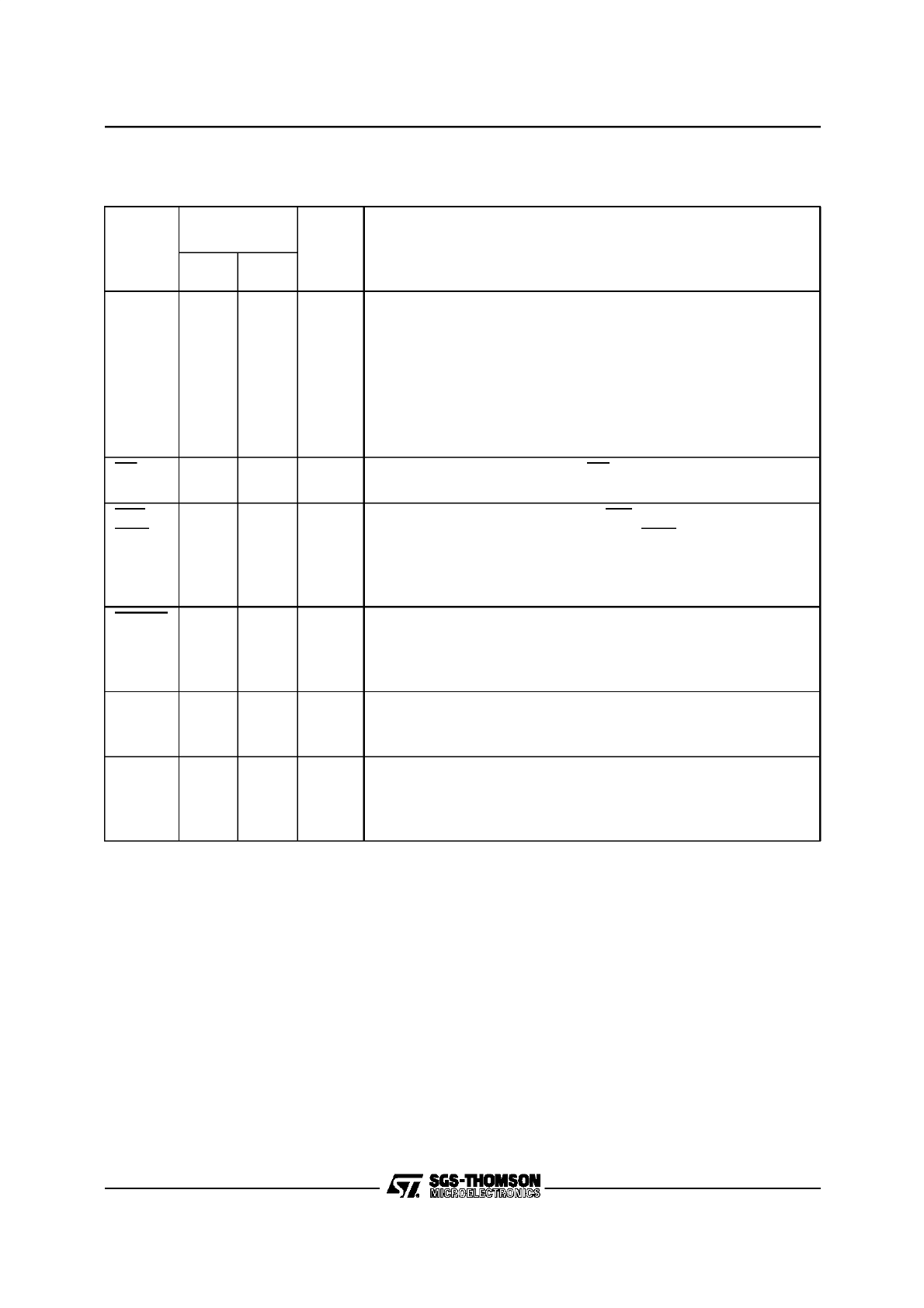
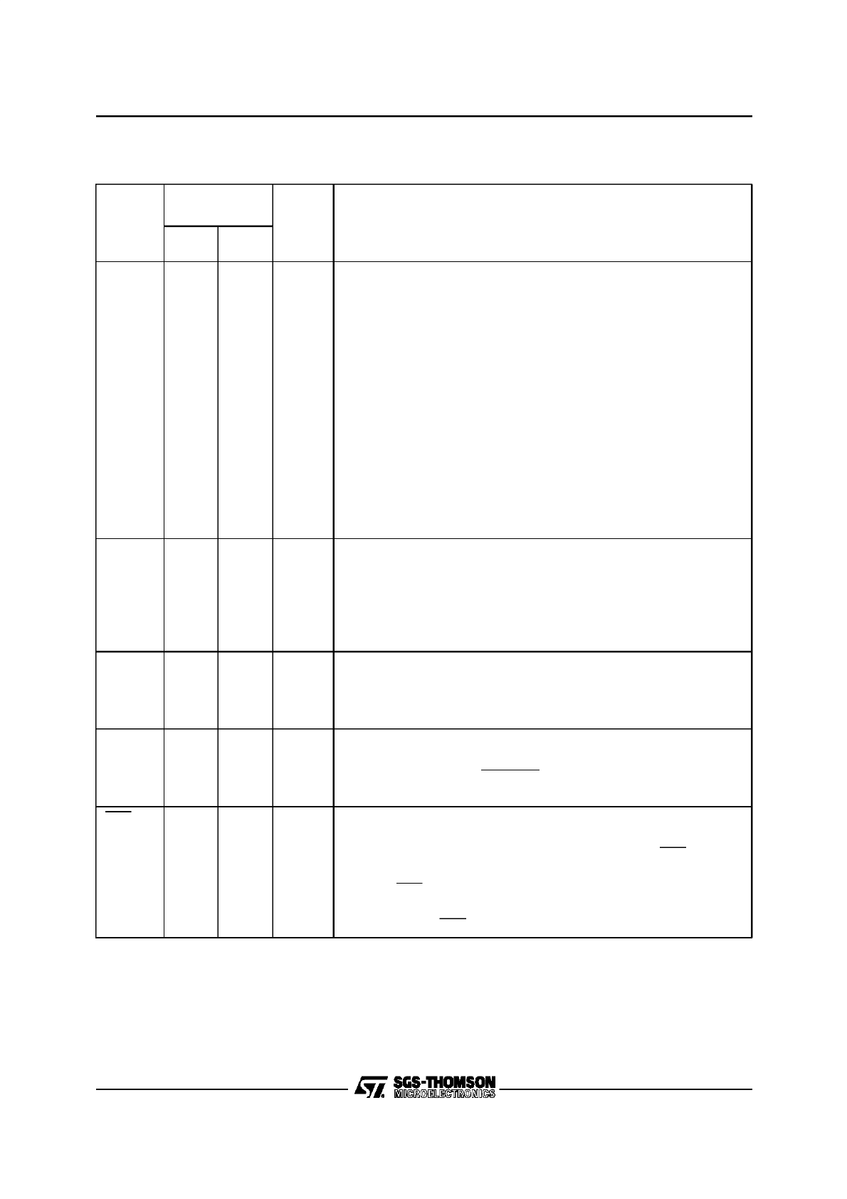
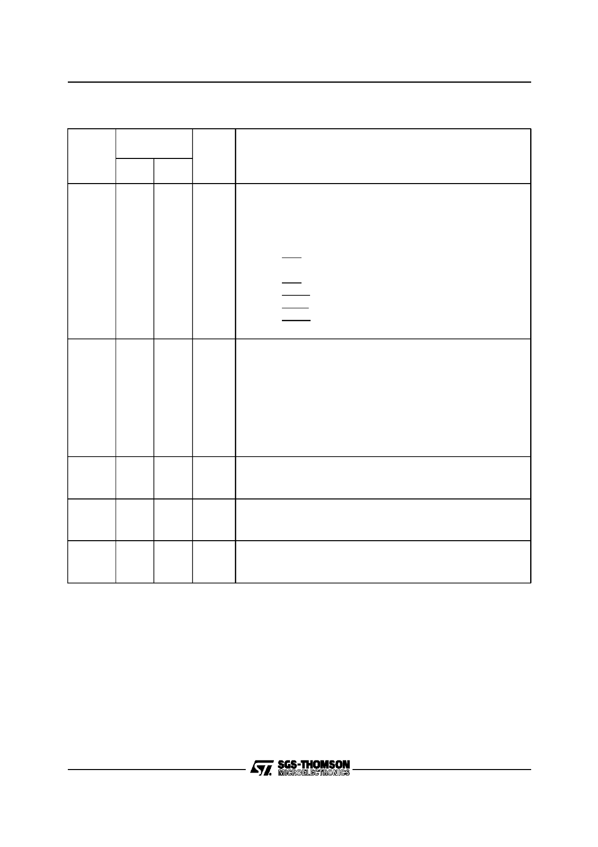
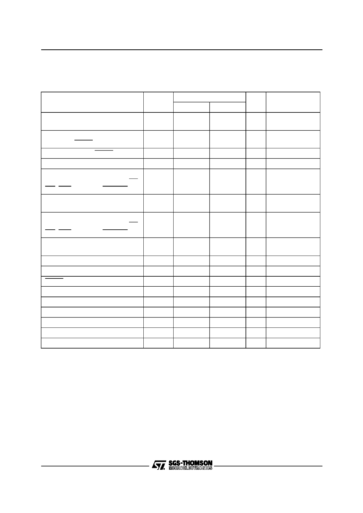
Table 1. Pin Definitions and Functions
Symbol
Pin
Number
Input
(I)
Output
(O)
Function
PQFP
TQFP
P5.10 –
P5.15
100
1 - 5
100
1
2
3
4
5
98
99 - 3
98
99
100
1
2
3
I
I
I
I
I
I
I
I
Port 5 is a 6-bit input-only port with Schmitt-Trigger characteris-
tics. The pins of Port 5 also serve as timer inputs:
P5.10
T6EUD GPT2 Timer T6 Ext.Up/Down Ctrl.Input
P5.11
T5EUD GPT2 Timer T5 Ext.Up/Down Ctrl.Input
P5.12
T6IN
GPT2 Timer T6 Count Input
P5.13
T5IN
GPT2 Timer T5 Count Input
P5.14
T4EUD GPT1 Timer T4 Ext.Up/Down Ctrl.Input
P5.15
T2EUD GPT1 Timer T2 Ext.Up/Down Ctrl.Input
XTAL1
XTAL2
7
8
5
6
I
O
XTAL1: Input to the oscillator amplifier and input to the internal
clock generator
XTAL2: Output of the oscillator amplifier circuit.
To clock the device from an external source, drive XTAL1, while
leaving XTAL2 unconnected. Minimum and maximum high/low
and rise/fall times specified in the AC Characteristics must be ob-
served.
P3.0 –
P3.13,
P3.15
10 –
23,
24
11
12
13
14
15
16
17
18
19
20
21
22
23
24
8
21
22
9
10
11
12
13
14
15
16
17
18
19
20
21
22
I/O
I/O
I/O
O
I
O
I
I
I
I
I/O
I/O
O
I/O
O
O
I/O
O
Port 3 is a 15-bit (P3.14 is missing) bidirectional I/O port. It is bit-
wise programmable for input or output via direction bits. For a pin
configured as input, the output driver is put into high-impedance
state. Port 3 outputs can be configured as push/pull or open drain
drivers.
The following Port 3 pins also serve for alternate functions:
P3.1
T6OUT
GPT2 Timer T6 Toggle Latch Output
P3.2
CAPIN
GPT2 Register CAPREL Capture Input
P3.3
T3OUT
GPT1 Timer T3 Toggle Latch Output
P3.4
T3EUD
GPT1 Timer T3 Ext.Up/Down Ctrl.Input
P3.5
T4IN
GPT1 Timer T4 Input for
Count/Gate/Reload/Capture
P3.6
T3IN
GPT1 Timer T3 Count/Gate Input
P3.7
T2IN
GPT1 Timer T2 Input for
Count/Gate/Reload/Capture
P3.8
MRST
SSC Master-Rec./Slave-Transmit I/O
P3.9
MTSR
SSC Master-Transmit/Slave-Rec. O/I
P3.10 T
×
D0
ASC0 Clock/Data Output (Asyn./Syn.)
P3.11 R
×
D0
ASC0 Data Input (Asyn.) or I/O (Syn.)
P3.12 BHE
Ext. Memory High Byte Enable Signal,
WRH
Ext. Memory High Byte Write Strobe
P3.13 SCLK
SSC Master Clock Outp./Slave Cl. Inp.
P3.15 CLKOUT System Clock Output (=CPU Clock)
ST10R165
7/53
P4.0 –
P4.7
25 -
28,
31 - 34
25
...
34
23 - 26
29 - 32
23
...
32
I/O
O
...
O
Port 4 is an 8-bit bidirectional I/O port. It is bit-wise programmable
for input or output via direction bits. For a pin configured as input,
the output driver is put into high-impedance state.
In case of an external bus configuration, Port 4 can be used to
output the segment address lines:
P4.0
A16
Least Significant Segment Addr. Line
...
...
...
P4.7
A23
Most Significant Segment Addr. Line
RD
35
33
O
External Memory Read Strobe. RD is activated for every external
instruction or data read access.
WR/
WRL
36
34
O
External Memory Write Strobe. In WR-mode this pin is activated
for every external data write access. In WRL-mode this pin is ac-
tivated for low byte data write accesses on a 16-bit bus, and for
every data write access on an 8-bit bus. See WRCFG in register
SYSCON for mode selection.
READY
37
35
I
Ready Input. When the Ready function is enabled, a high level at
this pin during an external memory access will force the insertion
of memory cycle time waitstates until the pin returns to a low lev-
el.
ALE
38
36
O
Address Latch Enable Output. Can be used for latching the ad-
dress into external memory or an address latch in the multiplexed
bus modes.
EA
39
37
I
External Access Enable pin. A low level at this pin during and af-
ter Reset forces the
ST10R165
to begin instruction execution
out of external memory. A high level forces execution out of the
internal ROM. The
ST10R165
must have this pin tied to ‘0’.
Symbol
Pin
Number
Input
(I)
Output
(O)
Function
PQFP
TQFP
Table 1. Pin Definitions and Functions (Cont’d)
8/53
ST10R165
PORT0:
P0L.0 –
P0L.7,
P0H.0 -
P0H.7
43 –
50
53 –
60
41
48
51
58
I/O
PORT0 consists of the two 8-bit bidirectional I/O ports P0L and
P0H. It is bit-wise programmable for input or output via direction
bits. For a pin configured as input, the output driver is put into
high-impedance state.
In case of an external bus configuration, PORT0 serves as the
address (A) and address/data (AD) bus in multiplexed bus modes
and as the data (D) bus in demultiplexed bus modes.
Demultiplexed bus modes:
Data Path Width:
8-bit
16-bit
P0L.0 – P0L.7:
D0 – D7
D0 - D7
P0H.0 – P0H.7:
I/O
D8 - D15
Multiplexed bus modes:
Data Path Width:
8-bit
16-bit
P0L.0 – P0L.7:
AD0 – AD7
AD0 - AD7
P0H.0 – P0H.7:
A8 - A15
AD8 - AD15
PORT1:
P1L.0 –
P1L.7,
P1H.0 -
P1H.7
61 -
68
69 -
70,
73 - 78
59
66
67 - 68
71 - 76
I/O
PORT1 consists of the two 8-bit bidirectional I/O ports P1L and
P1H. It is bit-wise programmable for input or output via direction
bits. For a pin configured as input, the output driver is put into
high-impedance state. PORT1 is used as the 16-bit address bus
(A) in demultiplexed bus modes and also after switching from a
demultiplexed bus mode to a multiplexed bus mode.
RSTIN
81
79
I
Reset Input with Schmitt-Trigger characteristics. A low level at
this pin for a specified duration while the oscillator is running re-
sets the
ST10R165
. An internal pullup resistor permits power-
on reset using only a capacitor connected to
V
SS
.
RSTOU
T
82
80
O
Internal Reset Indication Output. This pin is set to a low level
when the part is executing either a hardware-, a software- or a
watchdog timer reset. RSTOUT remains low until the EINIT (end
of initialization) instruction is executed.
NMI
83
81
I
Non-Maskable Interrupt Input. A high to low transition at this pin
causes the CPU to vector to the NMI trap routine. When the
PWRDN (power down) instruction is executed, the NMI pin must
be low in order to force the ST10R65 to go into power down
mode. If NMI is high, when PWRDN is executed, the part will con-
tinue to run in normal mode.
If not used, pin NMI should be pulled high externally.
Symbol
Pin
Number
Input
(I)
Output
(O)
Function
PQFP
TQFP
Table 1. Pin Definitions and Functions (Cont’d)
ST10R165
9/53
P6.0 –
P6.7
84 -
91
84
...
88
89
90
91
82 -
89
82
...
86
87
88
89
I/O
O
...
O
I
O
O
Port 6 is an 8-bit bidirectional I/O port. It is bit-wise programmable
for input or output via direction bits. For a pin configured as input,
the output driver is put into high-impedance state. Port 6 outputs
can be configured as push/pull or open drain drivers.
The following Port 6 pins also serve for alternate functions:
P6.0
CS0
Chip Select 0 Output
...
...
...
P6.4
CS4
Chip Select 4 Output
P6.5
HOLD
External Master Hold Request Input
P6.6
HLDA
Hold Acknowledge Output
P6.7
BREQ
Bus Request Output
P2.8 –
P2.15
92 -
99
92
...
99
90 -
97
90
...
97
I/O
I
...
I
Port 2 is an 8-bit bidirectional I/O port. It is bit-wise programmable
for input or output via direction bits. For a pin configured as input,
the output driver is put into high-impedance state. Port 2 outputs
can be configured as push/pull or open drain drivers.
The following Port 2 pins also serve for alternate functions:
P2.8
EX0IN
Fast External Interrupt 0 Input
...
...
...
P2.15
EX7IN
Fast External Interrupt 7 Input
V
PP
42
40
-
Flash programming voltage. This pin accepts the programming
voltage for flash versions of the
ST10R165
.
Note: This pin is not connected (NC) on non-flash versions.
V
DD
9, 30,
40, 51,
71, 80
7, 28,
38, 49,
69, 78
-
Digital Supply Voltage:
+ 5 V during normal operation and idle mode.
≥
2.5 V during power down mode
V
SS
6, 29,
41, 52,
72, 79
4, 27,
39, 50,
70, 77
-
Digital Ground.
Symbol
Pin
Number
Input
(I)
Output
(O)
Function
PQFP
TQFP
Table 1. Pin Definitions and Functions (Cont’d)
10/53
ST10R165
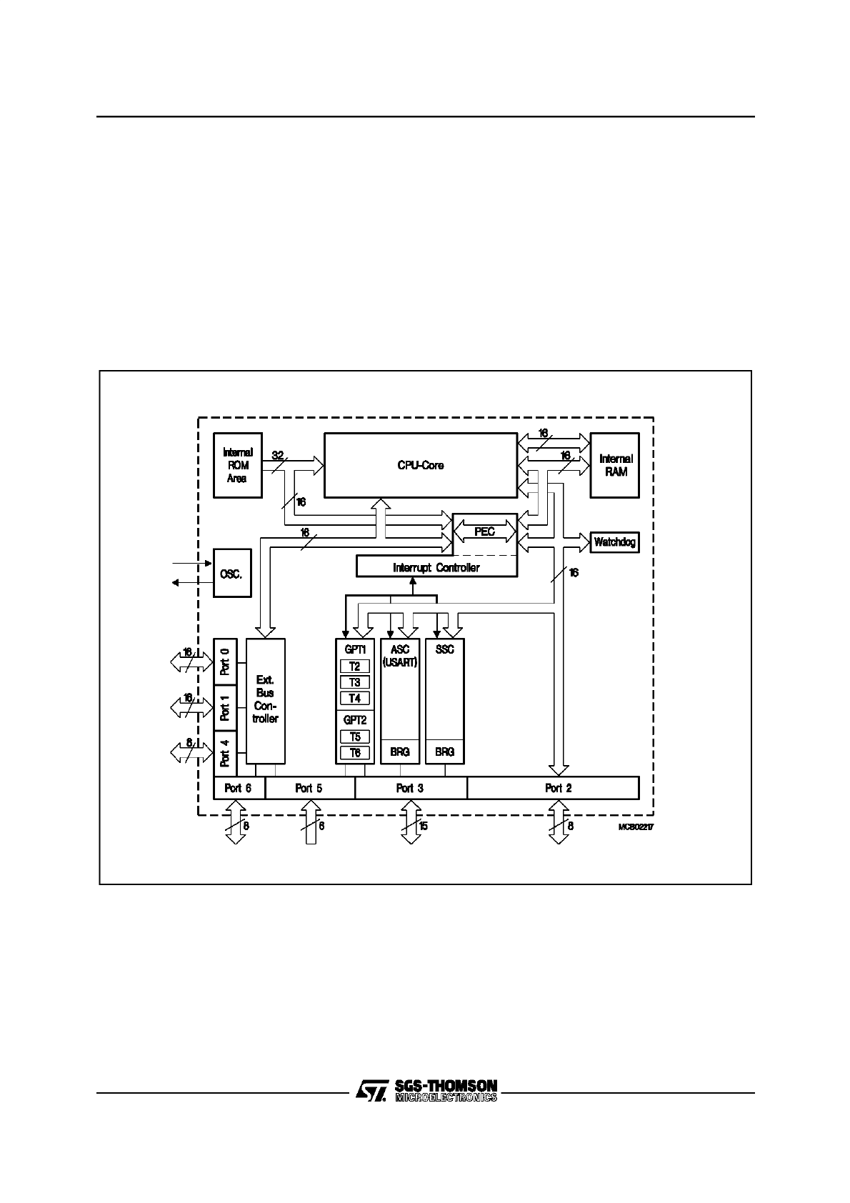
2 FUNCTIONAL DESCRIPTION
The architecture of the ST10R165 combines advantages of both RISC and CISC
processors and of advanced peripheral subsystems in a very well-balanced way. The
following block diagram gives an overview of the different on-chip components and of
the advanced, high bandwidth internal bus structure of the ST10R165.
Note: All time specifications refer to a CPU clock of 20 MHz (see definition in the AC
Characteristics section).
Figure 4. Block Diagram

ST10R165
11/53
3 MEMORY ORGANIZATION
The memory space of the ST10R165 is configured in a Von Neumann architecture
which means that code memory, data memory, registers and I/O ports are organized
within the same linear address space which includes 16 MBytes. The entire memory
space can be accessed bytewise or wordwise. Particular portions of the on-chip
memory have additionally been made directly bit addressable.The ST10R165 is pre-
pared to incorporate on-chip mask-programmable ROM for code or constant data.
Currently no ROM is integrated.
2 KBytes of on-chip RAM are provided as a storage for user defined variables, for the
system stack, general purpose register banks and even for code. A register bank can
consist of up to 16 wordwide (R0 to R15) and/or bytewide (RL0, RH0,
…
, RL7, RH7)
named General Purpose Registers (GPRs).
1024 bytes (2 * 512 bytes) of the address space are reserved for the Special Function
Register areas (SFR space and ESFR space). SFRs are wordwide registers which
are used for controlling and monitoring functions of the different on-chip units. Un-
used SFR addresses are reserved for future derivatives of the ST10R165.
In order to meet the needs of designs where more memory is required than is provid-
ed on chip, up to 16 MBytes of external RAM and/or ROM can be connected to the
microcontroller.

12/53
ST10R165
4 EXTERNAL BUS CONTROLLER
All of the external memory accesses are performed by a particular on-chip External
Bus Controller (EBC). It can be programmed either to Single Chip Mode when no ex-
ternal memory is required, or to one of four different external memory access modes,
which are as follows:
– 16-/18-/20-/24-bit Addresses, 16-bit Data, Demultiplexed
– 16-/18-/20-/24-bit Addresses, 16-bit Data, Multiplexed
– 16-/18-/20-/24-bit Addresses, 8-bit Data, Multiplexed
– 16-/18-/20-/24-bit Addresses, 8-bit Data, Demultiplexed
In the demultiplexed bus modes, addresses are output on PORT1 and data is input/
output on PORT0. In the multiplexed bus modes both addresses and data use
PORT0 for input/output.
Important timing characteristics of the external bus interface (Memory Cycle Time,
Memory Tri-State Time, Length of ALE and Read Write Delay) have been made pro-
grammable to allow the user the adoption of a wide range of different types of mem-
ories. In addition, different address ranges may be accessed with different bus char-
acteristics. Up to 5 external CS signals can be generated in order to save external
glue logic. Access to very slow memories is supported via a particular ‘Ready’ func-
tion. A HOLD/HLDA protocol is available for bus arbitration.
For applications which require less than 16 MBytes of external memory space, this
address space can be restricted to 1 MByte, 256 KByte or to 64 KByte. In this case
Port 4 outputs four, two or no address lines at all. It outputs all 8 address lines, if an
address space of 16 MBytes is used.
ST10R165
13/53
5 CENTRAL PROCESSING UNIT (CPU)
The main core of the CPU consists of a 4-stage instruction pipeline, a 16-bit arithme-
tic and logic unit (ALU) and dedicated SFRs. Additional hardware has been added for
a separate multiply and divide unit, a bit-mask generator and a barrel shifter.
Based on these hardware provisions, most of the ST10R165’s instructions can be ex-
ecuted in just one machine cycle which requires 100 ns at 20 MHz CPU clock. For ex-
ample, shift and rotate instructions are always processed during one machine cycle
independent of the number of bits to be shifted. All multiple-cycle instructions have
been optimized so that they can be executed very fast as well: branches in 2 cycles,
a 16
×
16 bit multiplication in 5 cycles and a 32/16 bit division in 10 cycles. Another
pipeline optimization, the named ‘Jump Cache’, allows reducing the execution time of
repeatedly performed jumps in a loop from 2 cycles to 1 cycle.
Figure 5. CPU Block Diagram
CPU
16
16
R 0
R 15
MDL
MDH
R0
General
Purpose
Registers
R 15
Code Seg. Ptr.
Mul./Div.-HW
Barrel-Shift
Bit-Mask Gen.
16-Bit
ALU
Exec. Unit
Instr. Ptr.
SP
STKOV
STKUN
SYSCON
PSW
ROM
not
Implemented
on the
ST10R165
Data Pg. Ptrs.
BUSCON 0
BUSCON 1
BUSCON 2
BUSCON 3
BUSCON 4
ADDRSEL 1
ADDRSEL 2
ADDRSEL 3
ADDRSEL 4
Instr. Reg.
4-Stage
Pipeline
Internal
RAM
2 KByte
32
VR02045B
16

14/53
ST10R165
Central Processing Unit (Cont’d)
The CPU includes an actual register context consisting of up to 16 wordwide GPRs
which are physically allocated within the on-chip RAM area. A Context Pointer (CP)
register determines the base address of the active register bank to be accessed by
the CPU at a time. The number of register banks is only restricted by the available in-
ternal RAM space. For easy parameter passing, a register bank may overlap others.
A system stack of up to 2048 bytes is provided as a storage for temporary data. The
system stack is allocated in the on-chip RAM area, and it is accessed by the CPU via
the stack pointer (SP) register. Two separate SFRs, STKOV and STKUN, are implic-
itly compared against the stack pointer value upon each stack access for the detec-
tion of a stack overflow or underflow.
The high performance offered by the hardware implementation of the CPU can effi-
ciently be utilized by a programmer via the highly efficient ST10R165 instruction set
which includes the following instruction classes:
– Arithmetic Instructions
– Logical Instructions
– Boolean Bit Manipulation Instructions
– Compare and Loop Control Instructions
– Shift and Rotate Instructions
– Prioritize Instruction
– Data Movement Instructions
– System Stack Instructions
– Jump and Call Instructions
– Return Instructions
– System Control Instructions
– Miscellaneous Instructions
The basic instruction length is either 2 or 4 bytes. Possible operand types are bits,
bytes and words. A variety of direct, indirect or immediate addressing modes are pro-
vided to specify the required operands.

ST10R165
15/53
6 INTERRUPT SYSTEM
With an interrupt response time within a range from just 250 ns to 600 ns (in case of
internal program execution), the ST10R165 is capable of reacting very fast to the oc-
currence of non-deterministic events.
The architecture of the ST10R165 supports several mechanisms for fast and flexible
response to service requests that can be generated from various sources internal or
external to the microcontroller. Any of these interrupt requests can be programmed to
being serviced by the Interrupt Controller or by the Peripheral Event Controller (PEC).
In contrast to a standard interrupt service where the current program execution is
suspended and a branch to the interrupt vector table is performed, just one cycle is
‘stolen’ from the current CPU activity to perform a PEC service. A PEC service im-
plies a single byte or word data transfer between any two memory locations with an
additional increment of either the PEC source or the destination pointer. An individual
PEC transfer counter is implicitly decremented for each PEC service except when
performing in the continuous transfer mode. When this counter reaches zero, a
standard interrupt is performed to the corresponding source related vector location.
PEC services are very well suited, for example, for supporting the transmission or re-
ception of blocks of data. The ST10R165 has 8 PEC channels each of which offers
such fast interrupt-driven data transfer capabilities.
A separate control register which contains an interrupt request flag, an interrupt ena-
ble flag and an interrupt priority bitfield exists for each of the possible interrupt sourc-
es. Via its related register, each source can be programmed to one of sixteen inter-
rupt priority levels. Once having been accepted by the CPU, an interrupt service can
only be interrupted by a higher prioritized service request. For the standard interrupt
processing, each of the possible interrupt sources has a dedicated vector location.
Fast external interrupt inputs are provided to service external interrupts with high pre-
cision requirements. These fast interrupt inputs feature programmable edge detec-
tion (rising edge, falling edge or both edges).
Software interrupts are supported by means of the ‘TRAP’ instruction in combination
with an individual trap (interrupt) number.
The following table shows all of the possible ST10R165 interrupt sources and the cor-
responding hardware-related interrupt flags, vectors, vector locations and trap (inter-
rupt) numbers:
Note: Four nodes in the table (X-Peripheral nodes) are prepared to accept interrupt requests
from integrated X-Bus peripherals. Nodes, where no X-Peripherals are connected, may
be used to generate software controlled interrupt requests by setting the respective XPnIR
bit. Also the three listed Software Nodes can be used for this purpose.
16/53
ST10R165
Interrupt System (Cont’d)
Source of Interrupt or
PEC Service Request
Request
Flag
Enable
Flag
Interrupt
Vector
Vector
Location
Trap
Number
External Interrupt 0
CC8IR
CC8IE
CC8INT
60h
18h
External Interrupt 1
CC9IR
CC9IE
CC9INT
64h
19h
External Interrupt 2
CC10IR
CC10IE
CC10INT
68h
1Ah
External Interrupt 3
CC11IR
CC11IE
CC11INT
6Ch
1Bh
External Interrupt 4
CC12IR
CC12IE
CC12INT
70h
1Ch
External Interrupt 5
CC13IR
CC13IE
CC13INT
74h
1Dh
External Interrupt 6
CC14IR
CC14IE
CC14INT
78h
1Eh
External Interrupt 7
CC15IR
CC15IE
CC15INT
7Ch
1Fh
GPT1 Timer 2
T2IR
T2IE
T2INT
88h
22h
GPT1 Timer 3
T3IR
T3IE
T3INT
8Ch
23h
GPT1 Timer 4
T4IR
T4IE
T4INT
90h
24h
GPT2 Timer 5
T5IR
T5IE
T5INT
94h
25h
GPT2 Timer 6
T6IR
T6IE
T6INT
98h
26h
GPT2 CAPREL Register
CRIR
CRIE
CRINT
9Ch
27h
ASC0 Transmit
S0TIR
S0TIE
S0TINT
A8h
2Ah
ASC0 Transmit Buffer
S0TBIR
S0TBIE
S0TBINT
11Ch
47h
ASC0 Receive
S0RIR
S0RIE
S0RINT
ACh
2Bh
ASC0 Error
S0EIR
S0EIE
S0EINT
B0h
2Ch
SSC Transmit
SCTIR
SCTIE
SCTINT
B4h
2Dh
SSC Receive
SCRIR
SCRIE
SCRINT
B8h
2Eh
SSC Error
SCEIR
SCEIE
SCEINT
BCh
2Fh
X-Peripheral Node 0
XP0IR
XP0IE
XP0INT
100h
40h
X-Peripheral Node 1
XP1IR
XP1IE
XP1INT
104h
41h
X-Peripheral Node 2
XP2IR
XP2IE
XP2INT
108h
42h
X-Peripheral Node 3
XP3IR
XP3IE
XP3INT
10Ch
43h
Software Node
CC29IR
CC29IE
CC29INT
110h
44h
Software Node
CC30IR
CC30IE
CC30INT
114h
45h
Software Node
CC31IR
CC31IE
CC31INT
118h
46h
ST10R165
17/53
Interrupt System (Cont’d)
The ST10R165 also provides an excellent mechanism to identify and to process ex-
ceptions or error conditions that arise during run-time, named ‘Hardware Traps’.
Hardware traps cause immediate non-maskable system reaction which is similar to a
standard interrupt service (branching to a dedicated vector table location). The occur-
rence of a hardware trap is additionally signified by an individual bit in the trap flag
register (TFR). Except when another higher prioritized trap service is in progress, a
hardware trap will interrupt any actual program execution. In turn, hardware trap serv-
ices can normally not be interrupted by standard or PEC interrupts.
The following table shows all of the possible exceptions or error conditions that can
arise during run-time:
Exception Condition
Trap
Flag
Trap
Vector
Vector
Location
Trap
Number
Trap
Priority
Reset Functions:
Hardware Reset
Software Reset
Watchdog Timer Overflow
RESET
RESET
RESET
00’0000
h
00’0000
h
00’0000
h
00
h
00
h
00
h
III
III
III
Class A Hardware Traps:
Non-Maskable Interrupt
Stack Overflow
Stack Underflow
NMI
STKOF
STKUF
NMITRAP
STOTRAP
STUTRAP
00’0008
h
00’0010
h
00’0018
h
02
h
04
h
06
h
II
II
II
Class B Hardware Traps:
Undefined Opcode
Protected Instruction
Fault
Illegal Word Operand
Access
Illegal Instruction Access
Illegal External Bus
Access
UNDOPC
PRTFLT
ILLOPA
ILLINA
ILLBUS
BTRAP
BTRAP
BTRAP
BTRAP
BTRAP
00’0028
h
00’0028
h
00’0028
h
00’0028
h
00’0028
h
0A
h
0A
h
0A
h
0A
h
0A
h
I
I
I
I
I
Reserved
[2C
h
– 3C
h
]
[0B
h
– 0F
h
]
Software Traps
TRAP Instruction
Any
[00’0000
h
–
00’01FC
h
]
in steps
of 4
h
Any
[00
h
– 7F
h
]
Current
CPU Priori-
ty

18/53
ST10R165
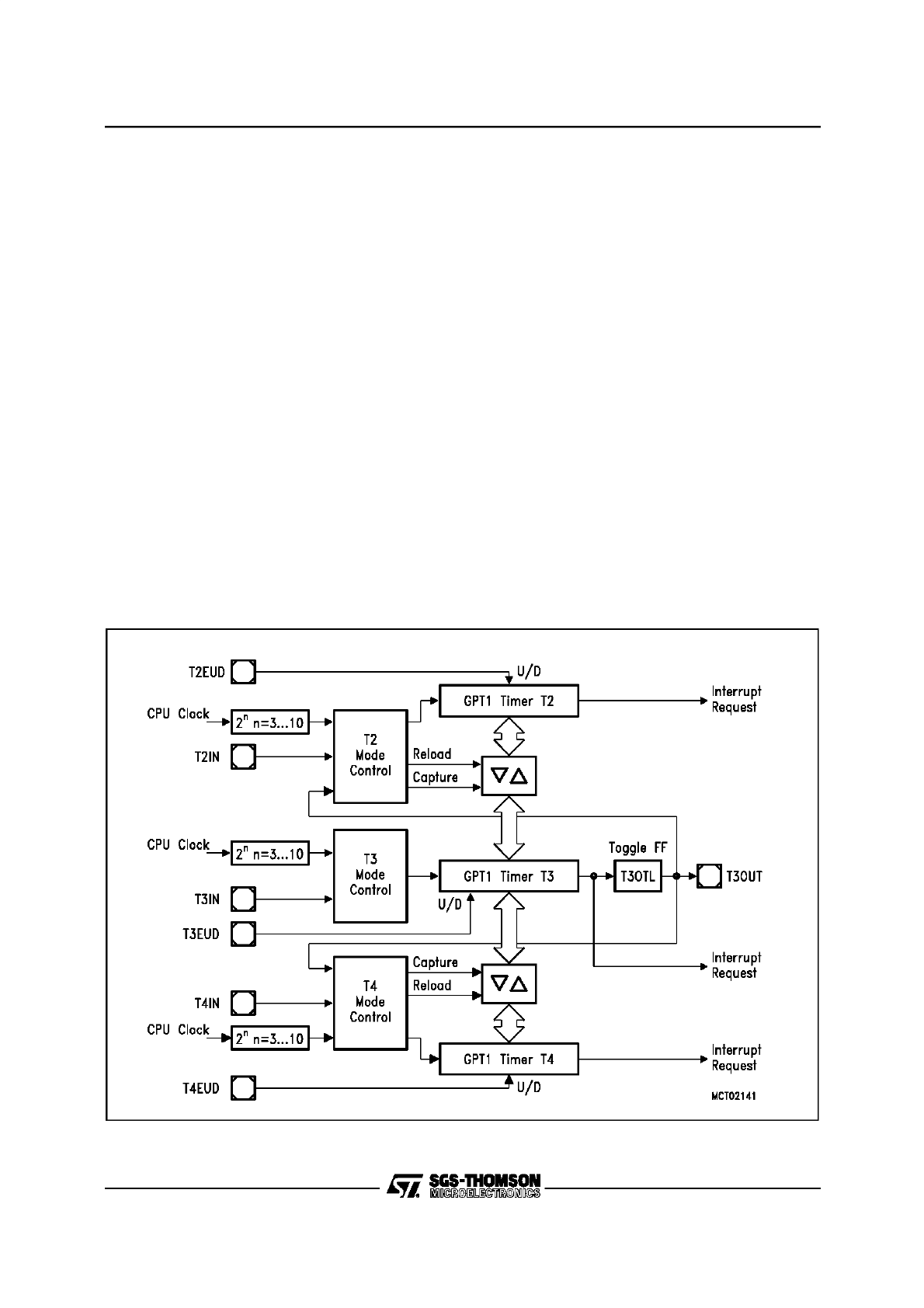
7 GENERAL PURPOSE TIMER (GPT) UNIT
The GPT unit represents a very flexible multifunctional timer/counter structure which
may be used for many different time related tasks such as event timing and counting,
pulse width and duty cycle measurements, pulse generation, or pulse multiplication.
The GPT unit incorporates five 16-bit timers which are organized in two separate
modules, GPT1 and GPT2. Each timer in each module may operate independently in
a number of different modes, or may be concatenated with another timer of the same
module.
Each of the three timers T2, T3, T4 of module GPT1 can be configured individually for
one of three basic modes of operation, which are Timer, Gated Timer, and Counter
Mode. In Timer Mode, the input clock for a timer is derived from the CPU clock, divid-
ed by a programmable prescaler, while Counter Mode allows a timer to be clocked in
reference to external events.
Pulse width or duty cycle measurement is supported in Gated Timer Mode, where the
operation of a timer is controlled by the ‘gate’ level on an external input pin. For these
purposes, each timer has one associated port pin (TxIN) which serves as gate or
clock input. The maximum resolution of the timers in module GPT1 is 400 ns (@ 20
MHz CPU clock).
The count direction (up/down) for each timer is programmable by software or may ad-
ditionally be altered dynamically by an external signal on a port pin (TxEUD) to facili-
tate e. g. position tracking.
Timers T3 and T4 have output toggle latches (TxOTL) which change their state on
each timer over-flow/underflow. The state of these latches may be output on port pins
(TxOUT) e. g. for time out monitoring of external hardware components, or may be
used internally to clock timers T2 and T4 for measuring long time periods with high
resolution.
In addition to their basic operating modes, timers T2 and T4 may be configured as re-
load or capture registers for timer T3. When used as capture or reload registers, tim-
ers T2 and T4 are stopped. The contents of timer T3 is captured into T2 or T4 in re-
sponse to a signal at their associated input pins (TxIN). Timer T3 is reloaded with the
contents of T2 or T4 triggered either by an external signal or by a selectable state
transition of its toggle latch T3OTL. When both T2 and T4 are configured to alternate-
ly reload T3 on opposite state transitions of T3OTL with the low and high times of a
PWM signal, this signal can be constantly generated without software intervention.
ST10R165
19/53
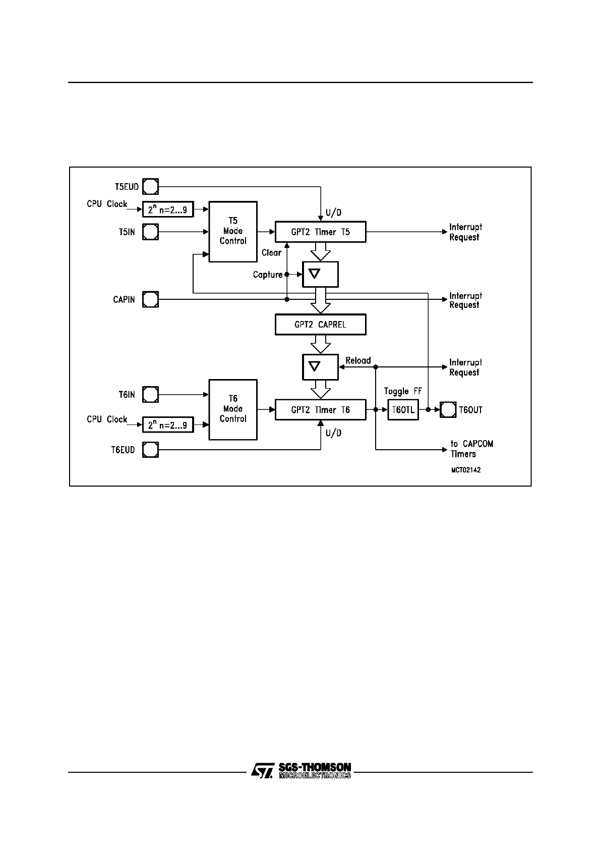
General Purpose Timer (GPT) Unit (Cont’d)
With its maximum resolution of 200 ns (@ 20 MHz), the GPT2 module provides pre-
cise event control and time measurement. It includes two timers (T5, T6) and a cap-
ture/reload register (CAPREL). Both timers can be clocked with an input clock which
is derived from the CPU clock via a programmable prescaler or with external signals.
The count direction (up/down) for each timer is programmable by software or may ad-
ditionally be altered dynamically by an external signal on a port pin (TxEUD). Con-
catenation of the timers is supported via the output toggle latch (T6OTL) of timer T6,
which changes its state on each timer overflow/underflow.
The state of this latch may be used to clock timer T5, or it may be output on a port pin
(T6OUT). The overflows/underflows of timer T6 can additionally be used to clock the
CAPCOM timers T0 or T1, and to cause a reload from the CAPREL register. The
CAPREL register may capture the contents of timer T5 based on an external signal
transition on the corresponding port pin (CAPIN), and timer T5 may optionally be
cleared after the capture procedure. This allows absolute time differences to be
measured or pulse multiplication to be performed without software overhead.
Figure 6. Block Diagram of GPT1
20/53
ST10R165
General Purpose Timer (GPT) Unit (Cont’d)
Figure 7. Block Diagram of GPT2

ST10R165
21/53
8 PARALLEL PORTS
The ST10R165 provides up to 77 I/O lines which are organized into six input/output
ports and one input port. All port lines are bit-addressable, and all input/output lines
are individually (bit-wise) programmable as inputs or outputs via direction registers.
The I/O ports are true bidirectional ports which are switched to high impedance state
when configured as inputs. The output drivers of three I/O ports can be configured
(pin by pin) for push/pull operation or open-drain operation via control registers. Dur-
ing the internal reset, all port pins are configured as inputs.
All port lines have programmable alternate input or output functions associated with
them. PORT0 and PORT1 may be used as address and data lines when accessing
external memory, while Port 4 outputs the additional segment address bits A23/19/
17...A16 in systems where segmentation is enabled to access more than 64KBytes of
memory. Port 6 provides optional bus arbitration signals (BREQ, HLDA, HOLD) and
chip select signals. Port 3 includes alternate functions of timers, serial interfaces, the
optional bus control signal BHE and the system clock output (CLKOUT). Port 5 is
used for timer control signals. All port lines that are not used for these alternate func-
tions may be used as general purpose I/O lines.
9 SERIAL CHANNELS
Serial communication with other microcontrollers, processors, terminals or external
peripheral components is provided by two serial interfaces with different functionality,
an Asynchronous/Synchronous Serial Channel (ASC0) and a High-Speed Synchro-
nous Serial Channel (SSC).
They support full-duplex asynchronous communication up to 625 KBaud and half-du-
plex synchronous communication up to 5 Mbaud (2.5 Mbaud on the ASC0) @ 20
MHz system clock.
Two dedicated baud rate generators allow to set up all standard baud rates without
oscillator tuning. For transmission, reception, and erroneous reception 3 separate in-
terrupt vectors are provided for each serial channel.
In asynchronous mode, 8- or 9-bit data frames are transmitted or received, preceded
by a start bit and terminated by one or two stop bits. For multiprocessor communica-
tion, a mechanism to distinguish address from data bytes has been included (8-bit
data + wake up bit mode).

22/53
ST10R165
Serial Channels (Cont’d)
In synchronous mode, the ASC0 transmits or receives bytes (8 bits) synchronously to
a shift clock which is generated by the ASC0. The SSC transmits or receives charac-
ters of 2...16 bits length synchronously to a shift clock which can be generated by the
SSC (master mode) or by an external master (slave mode). The SSC can start shift-
ing with the LSB or with the MSB, while the ASC0 always shifts the LSB first.
A loop back option is available for testing purposes.
A number of optional hardware error detection capabilities has been included to in-
crease the reliability of data transfers. A parity bit can automatically be generated on
transmission or be checked on reception. Framing error detection allows to recognize
data frames with missing stop bits. An overrun error will be generated, if the last char-
acter received has not been read out of the receive buffer register at the time the re-
ception of a new character is complete.
10 WATCHDOG TIMER
The Watchdog Timer represents one of the fail-safe mechanisms which have been
implemented to prevent the controller from malfunctioning for longer periods of time.
The Watchdog Timer is always enabled after a reset of the chip, and can only be dis-
abled in the time interval until the EINIT (end of initialization) instruction has been ex-
ecuted. Thus, the chip’s start-up procedure is always monitored. The software has to
be designed to service the Watchdog Timer before it overflows. If, due to hardware or
software related failures, the software fails to do so, the Watchdog Timer overflows
and generates an internal hardware reset and pulls the RSTOUT pin low in order to
allow external hardware components to be reset.
The Watchdog Timer is a 16-bit timer, clocked with the system clock divided either by
2 or by 128. The high byte of the Watchdog Timer register can be set to a pre-speci-
fied reload value (stored in WDTREL) in order to allow further variation of the moni-
tored time interval. Each time it is serviced by the application software, the high byte
of the Watchdog Timer is reloaded. Thus, time intervals between 25
µ
s and 420 ms
can be monitored (@ 20 MHz). The default Watchdog Timer interval after reset is
6.55 ms (@ 20 MHz).
ST10R165
23/53
11 INSTRUCTION SET SUMMARY
The table below lists the instructions of the ST10R165 in a condensed way.
The various addressing modes that can be used with a specific instruction, the oper-
ation of the instructions, parameters for conditional execution of instructions, and the
opcodes for each instruction can be found in the “ST10 Programming Manual”.
This document also provides a detailed description of each instruction.
Mnemonic
Description
Bytes
ADD(B)
Add word (byte) operands
2 / 4
ADDC(B)
Add word (byte) operands with Carry
2 / 4
SUB(B)
Subtract word (byte) operands
2 / 4
SUBC(B)
Subtract word (byte) operands with Carry
2 / 4
MUL(U)
(Un)Signed multiply direct GPR by direct GPR (16-16-bit)
2
DIV(U)
(Un)Signed divide register MDL by direct GPR (16-/16-bit)
2
DIVL(U)
(Un)Signed long divide reg. MD by direct GPR (32-/16-bit)
2
CPL(B)
Complement direct word (byte) GPR
2
NEG(B)
Negate direct word (byte) GPR
2
AND(B)
Bitwise AND, (word/byte operands)
2 / 4
OR(B)
Bitwise OR, (word/byte operands)
2 / 4
XOR(B)
Bitwise XOR, (word/byte operands)
2 / 4
BCLR
Clear direct bit
2
BSET
Set direct bit
2
BMOV(N)
Move (negated) direct bit to direct bit
4
BAND, BOR, BXOR
AND/OR/XOR direct bit with direct bit
4
BCMP
Compare direct bit to direct bit
4
BFLDH/L
Bitwise modify masked high/low byte of bit-addressable
direct word memory with immediate data
4
CMP(B)
Compare word (byte) operands
2 / 4
CMPD1/2
Compare word data to GPR and decrement GPR by 1/2
2 / 4
CMPI1/2
Compare word data to GPR and increment GPR by 1/2
2 / 4
PRIOR
Determine number of shift cycles to normalize direct
word GPR and store result in direct word GPR
2
SHL / SHR
Shift left/right direct word GPR
2
ROL / ROR
Rotate left/right direct word GPR
2
24/53
ST10R165
ASHR
Arithmetic (sign bit) shift right direct word GPR
2
MOV(B)
Move word (byte) data
2 / 4
MOVBS
Move byte operand to word operand with sign extension
2 / 4
MOVBZ
Move byte operand to word operand. with zero extension
2 / 4
JMPA, JMPI, JMPR
Jump absolute/indirect/relative if condition is met
4
JMPS
Jump absolute to a code segment
4
J(N)B
Jump relative if direct bit is (not) set
4
JBC
Jump relative and clear bit if direct bit is set
4
JNBS
Jump relative and set bit if direct bit is not set
4
CALLA, CALLI, CALLR
Call absolute/indirect/relative subroutine if condition is met
4
CALLS
Call absolute subroutine in any code segment
4
PCALL
Push direct word register onto system stack and call
absolute subroutine
4
TRAP
Call interrupt service routine via immediate trap number
2
PUSH, POP
Push/pop direct word register onto/from system stack
2
SCXT
Push direct word register onto system stack and update
register with word operand
4
RET
Return from intra-segment subroutine
2
RETS
Return from inter-segment subroutine
2
RETP
Return from intra-segment subroutine and pop direct
word register from system stack
2
RETI
Return from interrupt service subroutine
2
SRST
Software Reset
4
IDLE
Enter Idle Mode
4
PWRDN
Enter Power Down Mode
(supposes NMI-pin being low)
4
SRVWDT
Service Watchdog Timer
4
DISWDT
Disable Watchdog Timer
4
EINIT
Signify End-of-Initialization on RSTOUT-pin
4
ATOMIC
Begin ATOMIC sequence
2
EXTR
Begin EXTended Register sequence
2
EXTP(R)
Begin EXTended Page (and Register) sequence
2 / 4
EXTS(R)
Begin EXTended Segment (and Register) sequence
2 / 4
NOP
Null operation
2
Mnemonic
Description
Bytes
Instruction Set (Cont’d)
ST10R165
25/53
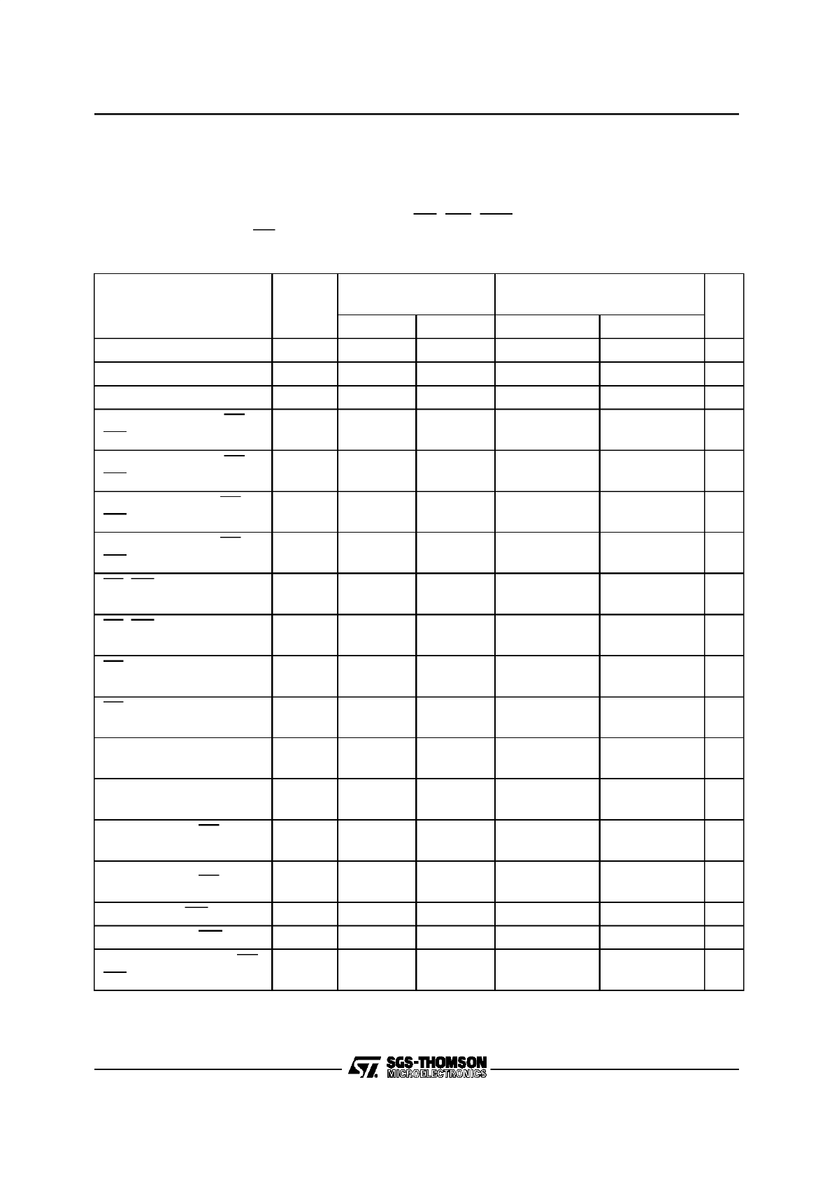
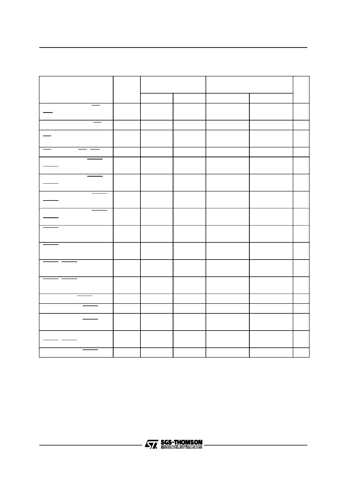
12 SPECIAL FUNCTION REGISTER OVERVIEW
The following table lists all SFRs which are implemented in the ST10R165 in alpha-
betical order.
Bit-addressable SFRs are marked with the letter “b” in column “Name”. SFRs within
the Extended SFR-Space (ESFRs) are marked with the letter “E” in column “Physi-
cal Address”.
An SFR can be specified via its individual mnemonic name. Depending on the select-
ed addressing mode, an SFR can be accessed via its physical address (using the
Data Page Pointers), or via its short 8-bit address (without using the Data Page Point-
ers).
Name
Physical
Address
8-Bit
Address
Description
Reset
Value
ADDRSEL1
FE18h
0Ch
Address Select Register 1
0000h
ADDRSEL2
FE1Ah
0Dh
Address Select Register 2
0000h
ADDRSEL3
FE1Ch
0Eh
Address Select Register 3
0000h
ADDRSEL4
FE1Eh
0Fh
Address Select Register 4
0000h
BUSCON0b
FF0Ch
86h
Bus Configuration Register 0
0XX0h
BUSCON1b
FF14h
8Ah
Bus Configuration Register 1
0000h
BUSCON2b
FF16h
8Bh
Bus Configuration Register 2
0000h
BUSCON3b
FF18h
8Ch
Bus Configuration Register 3
0000h
BUSCON4b
FF1Ah
8Dh
Bus Configuration Register 4
0000h
CAPREL
FE4Ah
25h
GPT2 Capture/Reload Register
0000h
CC8IC
b
FF88h
C4h
EX0IN Interrupt Control Register
0000h
CC9IC
b
FF8Ah
C5h
EX1IN Interrupt Control Register
0000h
CC10IC
b
FF8Ch
C6h
EX2IN Interrupt Control Register
0000h
CC11IC
b
FF8Eh
C7h
EX3IN Interrupt Control Register
0000h
CC12IC
b
FF90h
C8h
EX4IN Interrupt Control Register
0000h
CC13IC
b
FF92h
C9h
EX5IN Interrupt Control Register
0000h
CC14IC
b
FF94h
CAh
EX6IN Interrupt Control Register
0000h
CC15IC
b
FF96h
CBh
EX7IN Interrupt Control Register
0000h
CC29IC
b
F184h
E
C2h
Software Node Interrupt Control Register
0000h
CC30IC
b
F18Ch
E
C6h
Software Node Interrupt Control Register
0000h
CC31IC
b
F194h
E
CAh
Software Node Interrupt Control Register
0000h
CP
FE10h
08h
CPU Context Pointer Register
FC00h
26/53
ST10R165
CRIC
b
FF6Ah
B5h
GPT2 CAPREL Interrupt Control Register
0000h
CSP
FE08h
04h
CPU Code Segment Pointer Register (read only)
0000h
DP0L
b
F100h
E
80h
P0L Direction Control Register
00h
DP0H
b
F102h
E
81h
P0h Direction Control Register
00h
DP1L
b
F104h
E
82h
P1L Direction Control Register
00h
DP1H
b
F106h
E
83h
P1h Direction Control Register
00h
DP2
b
FFC2h
E1h
Port 2 Direction Control Register
0000h
DP3
b
FFC6h
E3h
Port 3 Direction Control Register
0000h
DP4
b
FFCAh
E5h
Port 4 Direction Control Register
00h
DP6
b
FFCEh
E7h
Port 6 Direction Control Register
00h
DPP0
FE00h
00h
CPU Data Page Pointer 0 Register (10 bits)
0000h
DPP1
FE02h
01h
CPU Data Page Pointer 1 Register (10 bits)
0001h
DPP2
FE04h
02h
CPU Data Page Pointer 2 Register (10 bits)
0002h
DPP3
FE06h
03h
CPU Data Page Pointer 3 Register (10 bits)
0003h
EXICON
b
F1C0h
E
E0h
External Interrupt Control Register
0000h
MDC
b
FF0Eh
87h
CPU Multiply Divide Control Register
0000h
MDH
FE0Ch
06h
CPU Multiply Divide Register – High Word
0000h
MDL
FE0Eh
07h
CPU Multiply Divide Register – Low Word
0000h
ODP2
b
F1C2h
E
E1h
Port 2 Open Drain Control Register
0000h
ODP3
b
F1C6h
E
E3h
Port 3 Open Drain Control Register
0000h
ODP6
b
F1CEh
E
E7h
Port 6 Open Drain Control Register
00h
ONES
FF1Eh
8Fh
Constant Value 1’s Register (read only)
FFFFh
P0L
b
FF00h
80h
Port 0 Low Register (Lower half of PORT0)
00h
P0H
b
FF02h
81h
Port 0 High Register (Upper half of PORT0)
00h
P1L
b
FF04h
82h
Port 1 Low Register (Lower half of PORT1)
00h
P1H
b
FF06h
83h
Port 1 High Register (Upper half of PORT1)
00h
P2
b
FFC0h
E0h
Port 2 Register
0000h
P3
b
FFC4h
E2h
Port 3 Register
0000h
P4
b
FFC8h
E4h
Port 4 Register (8 bits)
00h
P5
b
FFA2h
D1h
Port 5 Register (read only)
XXXXh
P6
b
FFCCh
E6h
Port 6 Register (8 bits)
00h
PECC0
FEC0h
60h
PEC Channel 0 Control Register
0000h
Name
Physical
Address
8-Bit
Address
Description
Reset
Value
Special Function Register Overview
(Cont’d)
ST10R165
27/53
PECC1
FEC2h
61h
PEC Channel 1 Control Register
0000h
PECC2
FEC4h
62h
PEC Channel 2 Control Register
0000h
PECC3
FEC6h
63h
PEC Channel 3 Control Register
0000h
PECC4
FEC8h
64h
PEC Channel 4 Control Register
0000h
PECC5
FECAh
65h
PEC Channel 5 Control Register
0000h
PECC6
FECCh
66h
PEC Channel 6 Control Register
0000h
PECC7
FECEh
67h
PEC Channel 7 Control Register
0000h
PSW
b
FF10h
88h
CPU Program Status Word
0000h
RP0H
b
F108h
E
84h
System Start-up Configuration Register (Rd. only)
XXh
S0BG
FEB4h
5Ah
Serial Channel 0 Baud Rate Generator Reload Reg-
ister
0000h
S0CON
b
FFB0h
D8h
Serial Channel 0 Control Register
0000h
S0EIC
b
FF70h
B8h
Serial Channel 0 Error Interrupt Control Register
0000h
S0RBUF
FEB2h
59h
Serial Channel 0 Receive Buffer Register
(read only)
XXh
S0RIC
b
FF6Eh
B7h
Serial Channel 0 Receive Interrupt Control Register
0000h
S0TBIC
b
F19Ch
E
CEh
Serial Channel 0 Transmit Buffer Interrupt Control
Register
0000h
S0TBUF
FEB0h
58h
Serial Channel 0 Transmit Buffer Register
(write only)
00h
S0TIC
b
FF6Ch
B6h
Serial Channel 0 Transmit Interrupt Control Register
0000h
SP
FE12h
09h
CPU System Stack Pointer Register
FC00h
SSCBR
F0B4h
E
5Ah
SSC Baudrate Register
0000h
SSCCON b
FFB2h
D9h
SSC Control Register
0000h
SSCEIC
b
FF76h
BBh
SSC Error Interrupt Control Register
0000h
SSCRB
F0B2h
E
59h
SSC Receive Buffer (read only)
XXXXh
SSCRIC
b
FF74h
BAh
SSC Receive Interrupt Control Register
0000h
SSCTB
F0B0h
E
58h
SSC Transmit Buffer (write only)
0000h
SSCTIC
b
FF72h
B9h
SSC Transmit Interrupt Control Register
0000h
STKOV
FE14h
0Ah
CPU Stack Overflow Pointer Register
FA00h
STKUN
FE16h
0Bh
CPU Stack Underflow Pointer Register
FC00h
SYSCON b
FF12h
89h
CPU System Configuration Register
0xx0h*)
T2
FE40h
20h
GPT1 Timer 2 Register
0000h
T2CON
b
FF40h
A0h
GPT1 Timer 2 Control Register
0000h
Name
Physical
Address
8-Bit
Address
Description
Reset
Value
Special Function Register Overview
(Cont’d)
28/53
ST10R165
*) The system configuration is selected during reset.
Note: The Interrupt Control Registers XPnIC are prepared to control interrupt requests from
integrated X-Bus peripherals. Nodes, where no X-Peripherals are connected, may be
used to generate software controlled interrupt requests by setting the respective XPnIR
bit.
T2IC
b
FF60h
B0h
GPT1 Timer 2 Interrupt Control Register
0000h
T3
FE42h
21h
GPT1 Timer 3 Register
0000h
T3CON
b
FF42h
A1h
GPT1 Timer 3 Control Register
0000h
T3IC
b
FF62h
B1h
GPT1 Timer 3 Interrupt Control Register
0000h
T4
FE44h
22h
GPT1 Timer 4 Register
0000h
T4CON
b
FF44h
A2h
GPT1 Timer 4 Control Register
0000h
T4IC
b
FF64h
B2h
GPT1 Timer 4 Interrupt Control Register
0000h
T5
FE46h
23h
GPT2 Timer 5 Register
0000h
T5CON
b
FF46h
A3h
GPT2 Timer 5 Control Register
0000h
T5IC
b
FF66h
B3h
GPT2 Timer 5 Interrupt Control Register
0000h
T6
FE48h
24h
GPT2 Timer 6 Register
0000h
T6CON
b
FF48h
A4h
GPT2 Timer 6 Control Register
0000h
T6IC
b
FF68h
B4h
GPT2 Timer 6 Interrupt Control Register
0000h
TFR
b
FFACh
D6h
Trap Flag Register
0000h
WDT
FEAEh
57h
Watchdog Timer Register (read only)
0000h
WDTCON
FFAEh
D7h
Watchdog Timer Control Register
0000h
XP0IC
b
F186h
E
C3h
X-Peripheral 0 Interrupt Control Register
0000h
XP1IC
b
F18Eh
E
C7h
X-Peripheral 1 Interrupt Control Register
0000h
XP2IC
b
F196h
E
CBh
X-Peripheral 2 Interrupt Control Register
0000h
XP3IC
b
F19Eh
E
CFh
X-Peripheral 3 Interrupt Control Register
0000h
ZEROS
b
FF1Ch
8Eh
Constant Value 0’s Register (read only)
0000h
Name
Physical
Address
8-Bit
Address
Description
Reset
Value
Special Function Register Overview
(Cont’d)

ST10R165
29/53
13 ELECTRICAL CHARACTERISTICS
13.1 Absolute Maximum Ratings
– Ambient temperature under bias (
T
A
): 0 to +70
°
C
– Storage temperature (
T
ST
):– 65 to +150
°
C
– Voltage on
V
DD
pins with respect to ground (
V
SS
): 0.5 to +6.5 V
– Voltage on any pin with respect to ground (
V
SS
): –0.5 to
V
DD
+0.5 V
– Input current on any pin during overload condition: –10 to +10 mA
– Absolute sum of all input currents during overload condition:|100 mA|
– Power dissipation:1.5 W
Note: Stresses above those listed under “Absolute Maximum Ratings” may cause permanent
damage to the device. This is a stress rating only and functional operation of the device at
these or any other conditions above those indicated in the operational sections of this
specification is not implied. Exposure to absolute maximum rating conditions for extended
periods may affect device reliability. During overload conditions (
V
IN
>
V
DD
or
V
IN
<
V
SS
) the
voltage on pins with respect to ground (
V
SS
) must not exceed the values defined by the
Absolute Maximum Ratings.
13.2 Parameter Interpretation
The parameters listed in the following partly represent the characteristics of the
ST10R165 and partly its demands on the system. To aid in interpreting the parame-
ters right, when evaluating them for a design, they are marked in column “Symbol”:
CC (Controller Characteristics):
The logic of the ST10R165 will provide signals with the respective timing characteris-
tics.
SR (System Requirement):
The external system must provide signals with the respective timing characteristics to
the ST10R165.
30/53
ST10R165
13.3 DC Characteristics
V
DD
= 5 V
±
10%;
V
SS
= 0 V; f
CPU
= 20 MHz; Reset active.
T
A
= 0 to +70
°
C
Parameter
Symbol
Limit Values
Unit
Test Condition
min.
max.
Input low voltage
V
IL
SR
– 0.5
0.2
V
DD
– 0.1
V
–
Input high voltage
(all except RSTIN and XTAL1)
V
IH
SR
0.2
V
DD
+ 0.9
V
DD
+ 0.5
V
–
Input high voltage RSTIN
V
IH1
SR
0.6
V
DD
V
DD
+ 0.5
V
–
Input high voltage XTAL1
V
IH2
SR
0.7
V
DD
V
DD
+ 0.5
V
–
Output low voltage
(PORT0, PORT1, Port 4, ALE, RD,
WR, BHE, CLKOUT, RSTOUT)
V
OL
CC
–
0.45
V
I
OL
= 2.4 mA
Output low voltage
(all other outputs)
V
OL1
CC
–
0.45
V
I
OL1
= 1.6 mA
Output high voltage
(PORT0, PORT1, Port 4, ALE, RD,
WR, BHE, CLKOUT, RSTOUT)
V
OH
CC
0.9
V
DD
2.4
–
V
I
OH
= – 500
µ
A
I
OH
= – 2.4 mA
Output high voltage
1)
(all other outputs)
V
OH1
CC
0.9
V
DD
2.4
–
V
V
I
OH
= – 250
µ
A
I
OH
= – 1.6 mA
Input leakage current
(Port 5)
I
OZ1
CC
–
±
200
nA
0 V <
V
IN
<
V
DD
Input leakage current (all other)
I
OZ2
CC
–
±
500
nA
0 V <
V
IN
<
V
DD
RSTIN pull-up resistor
R
RST
CC
50
150
k
Ω
–
Read/Write inactive current
4)
I
RWH
2)
–
-40
µ
A
V
OUT
= 2.4 V
Read/Write active current
4)
I
RWL
3)
-500
–
µ
A
V
OUT
=
V
OLmax
ALE inactive current
4)
I
ALEL
2)
–
40
µ
A
V
OUT
=
V
OLmax
ALE active current
4)
I
ALEH
3)
500
–
µ
A
V
OUT
= 2.4 V
Port 6 inactive current
4)
I
P6H
2)
–
-40
µ
A
V
OUT
= 2.4 V
Port 6 active current
4)
I
P6L
3)
-500
–
µ
A
V
OUT
=
V
OL1max
ST10R165
31/53
Notes:
1)
This specification is not valid for outputs which are switched to open drain mode. In this case
the respective output will float and the voltage results from the external circuitry.
2)
The maximum current may be drawn while the respective signal line remains inactive.
3)
The minimum current must be drawn in order to drive the respective signal line active.
4)
This specification is only valid during Reset, or during Hold- or Adapt-mode. Port 6 pins are
only affected, if they are used for CS output and the open drain function is not enabled.
5)
Not 100% tested, guaranteed by design characterization.
6)
The supply current is a function of the operating frequency. This dependency is illustrated in
the figure below.
These parameters are tested at V
DDmax
and 20 MHz CPU clock with all outputs discon-
nected and all inputs at V
IL
or V
IH
.
7)
This parameter is tested including leakage currents. All inputs (including pins configured as
inputs) at 0 V to 0.1 V or at V
DD
– 0.1 V to V
DD
, V
REF
= 0 V, all outputs (including pins config-
ured as outputs) disconnected.
PORT0 configuration current
4)
I
P0H
2)
–
-10
µ
A
V
IN
=
V
IHmin
I
P0L
3)
-100
–
µ
A
V
IN
=
V
ILmax
XTAL1 input current
I
IL
CC
–
±
20
µ
A
0 V <
V
IN
<
V
DD
Pin capacitance
5)
(digital inputs/outputs)
C
IO
CC
–
10
pF
f
= 1 MHz
T
A
= 25
°
C
Power supply current
I
CC
–
10 +
4 * f
CPU
mA
RSTIN =
V
IL2
f
CPU
in [MHz]
6)
Idle mode supply current
I
ID
–
2 +
1.2 * f
CPU
mA
RSTIN =
V
IH1
f
CPU
in [MHz]
6)
Power-down mode supply current
I
PD
–
100
µ
A
V
DD
= 5.5 V
7)
Parameter
Symbol
Limit Values
Unit
Test Condition
min.
max.
DC Characteristics (Cont’d)
V
DD
= 5 V
±
10%;
V
SS
= 0 V; f
CPU
= 20 MHz; Reset active.
T
A
= 0 to +70
°
C
32/53
ST10R165
DC Characteristics (Cont’d)
Figure 8. Supply/Idle Current as a Function of Operating Frequency
I
[mA]
f
CPU
[MHz]
5
10
15
20
150
100
50
10
I
CCmax
I
IDmax
ST10R165
33/53
13.4 Testing Waveforms
Figure 9. Input Output Waveforms
Figure 10. Float Waveforms
AC inputs during testing are driven at 2.4 V for a log-
For timing purposes a port pin is no longer floating
when a 100 mV change from load
34/53
ST10R165
13.5 AC Characteristics
External Clock Drive XTAL1
V
DD
= 5 V
±
10%;
V
SS
= 0 V
T
A
= 0 to +70
°
C
Figure 11. External Clock Drive XTAL1
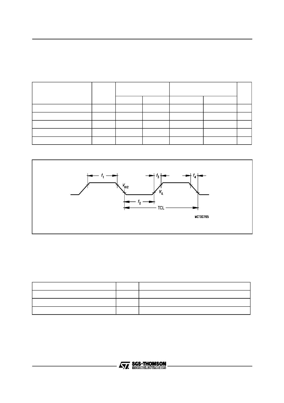
13.5.1 Memory Cycle Variables
The timing tables below use three variables which are derived from the BUSCONx
registers and represent the special characteristics of the programmed memory cycle.
The following table describes, how these variables are to be computed.
Parameter
Symbol
Max. CPU Clock
= 20 MHz
Variable CPU Clock
1/2TCL = 1 to 20 MHz
Unit
min.
max.
min.
max.
Oscillator period
TCL SR
25
25
25
500
ns
High time
t
1
SR
6
–
6
–
ns
Low time
t
2
SR
6
–
6
–
ns
Rise time
t
3
SR
–
5
–
5
ns
Fall time
t
4
SR
–
5
–
5
ns
Description
Symbol
Values
ALE Extension
t
A
TCL * <ALECTL>
Memory Cycle Time Waitstates
t
C
2TCL * (15 - <MCTC>)
Memory Tristate Time
t
F
2TCL * (1 - <MTTC>)
ST10R165
35/53
13.5.2 Multiplexed Bus
V
DD
= 5 V
±
10%;
V
SS
= 0 V
T
A
= 0 to +70
°
C
C
L
(for PORT0, PORT1, Port 4, ALE, RD, WR, BHE, CLKOUT) = 100 pF
C
L
(for Port 6, CS) = 100 pF
ALE cycle time = 6 TCL + 2
t
A
+
t
C
+
t
F
(150 ns at 20-MHz CPU clock without waitstates)
Parameter
Symbol
Max. CPU Clock
= 20 MHz
Variable CPU Clock
1/2TCL = 1 to 20 MHz
Unit
min.
max.
min.
max.
ALE high time
t
5
CC
15 +
t
A
–
TCL - 10 +
t
A
–
ns
Address setup to ALE
t
6
CC
10 +
t
A
–
TCL - 15 +
t
A
–
ns
Address hold after ALE
t
7
CC
15 +
t
A
–
TCL - 10 +
t
A
–
ns
ALE falling edge to RD,
WR (with RW-delay)
t
8
CC
15 +
t
A
–
TCL - 10 +
t
A
–
ns
ALE falling edge to RD,
WR (no RW-delay)
t
9
CC
-10 +
t
A
–
-10 +
t
A
–
ns
Address float after RD,
WR (with RW-delay)
t
10
CC
–
5
–
5
ns
Address float after RD,
WR (no RW-delay)
t
11
CC
–
30
–
TCL + 5
ns
RD, WR low time
(with RW-delay)
t
12
CC
40 +
t
C
–
2TCL - 10 +
t
C
–
ns
RD, WR low time
(no RW-delay)
t
13
CC
65 +
t
C
–
3TCL - 10 +
t
C
–
ns
RD to valid data in
(with RW-delay)
t
14
SR
–
30 +
t
C
–
2TCL - 20 +
t
C
ns
RD to valid data in
(no RW-delay)
t
15
SR
–
55 +
t
C
–
3TCL - 20 +
t
C
ns
ALE low to valid data in
t
16
SR
–
55
+
t
A
+
t
C
–
3TCL - 20
+
t
A
+
t
C
ns
Address to valid data in
t
17
SR
–
70
+ 2
t
A
+
t
C
–
4TCL - 30
+ 2
t
A
+
t
C
ns
Data hold after RD
rising edge
t
18
SR
0
–
0
–
ns
Data float after RD
t
19
SR
–
35 +
t
F
–
2TCL - 15
+
t
F
ns
Data valid to WR
t
22
SR
35 +
t
C
–
2TCL - 15 +
t
C
–
ns
Data hold after WR
t
23
CC
35 +
t
F
–
2TCL - 15 +
t
F
–
ns
ALE rising edge after RD,
WR
t
25
CC
35 +
t
F
–
2TCL - 15 +
t
F
–
ns
36/53
ST10R165
Address hold after RD,
WR
t
27
CC
35 +
t
F
–
2TCL - 15 +
t
F
–
ns
ALE falling edge to CS
t
38
CC
-5 -
t
A
10 -
t
A
-5 -
t
A
10 -
t
A
ns
CS low to Valid Data In
t
39
SR
–
55 +
t
C
+
2
t
A
–
3TCL - 20
+
t
C
+ 2
t
A
ns
CS hold after RD, WR
t
40
CC
60 +
t
F
–
3TCL - 15 +
t
F
–
ns
ALE fall. edge to RdCS,
WrCS (with RW delay)
t
42
CC
20 +
t
A
–
TCL - 5 +
t
A
–
ns
ALE fall. edge to RdCS,
WrCS (no RW delay)
t
43
CC
-5 +
t
A
–
-5 +
t
A
–
ns
Address float after RdCS,
WrCS (with RW delay)
t
44
CC
–
0
–
0
ns
Address float after RdCS,
WrCS (no RW delay)
t
45
CC
–
25
–
TCL
ns
RdCS to Valid Data In
(with RW delay)
t
46
SR
–
25 +
t
C
–
2TCL - 25
+
t
C
ns
RdCS to Valid Data In
(no RW delay)
t
47
SR
–
50 +
t
C
–
3TCL - 25
+
t
C
ns
RdCS, WrCS Low Time
(with RW delay)
t
48
CC
40 +
t
C
–
2TCL - 10 +
t
C
–
ns
RdCS, WrCS Low Time
(no RW delay)
t
49
CC
65 +
t
C
–
3TCL - 10 +
t
C
–
ns
Data valid to WrCS
t
50
CC
35 +
t
C
–
2TCL - 15 +
t
C
–
ns
Data hold after RdCS
t
51
SR
0
–
0
–
ns
Data float after RdCS
t
52
SR
–
30 +
t
F
–
2TCL - 20
+
t
F
ns
Address hold after
RdCS, WrCS
t
54
CC
30 +
t
F
–
2TCL - 20 +
t
F
–
ns
Data hold after WrCS
t
56
CC
30 +
t
F
–
2TCL - 20 +
t
F
–
ns
Parameter
Symbol
Max. CPU Clock
= 20 MHz
Variable CPU Clock
1/2TCL = 1 to 20 MHz
Unit
min.
max.
min.
max.
Multiplexed Bus (Cont’d)
ST10R165
37/53
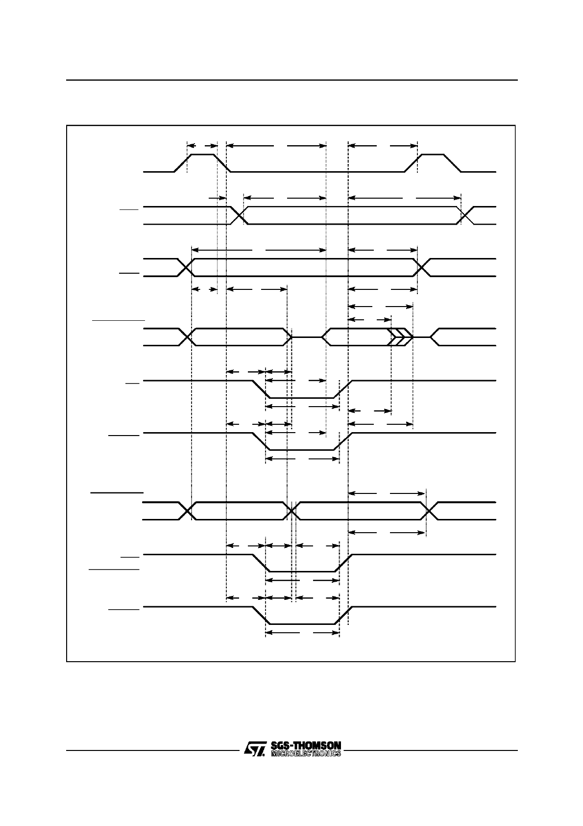
Figure 12. External Memory Cycle: Multiplexed Bus, With Read/Write Delay, Normal ALE
Data In
Data Out
Address
Address
t
38
t
44
t
10
Address
ALE
CSx
A23-A16
(A15-A8)
BHE
BUS
Read Cycle
RD
RdCSx
BUS
Write Cycle
WR,
WRL, WRH
WrCSx
t
5
t
16
t
17
t
6
t
7
t
39
t
40
t
25
t
27
t
18
t
19
t
14
t
46
t
12
t
48
t
10
t
22
t
23
t
44
t
12
t
48
t
8
t
42
t
42
t
8
t
50
t
51
t
54
t
52
t
56
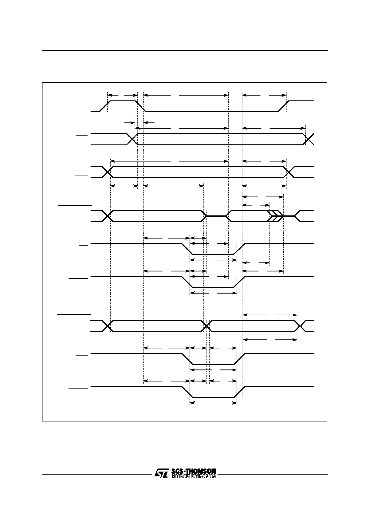
38/53
ST10R165
Figure 13. External Memory Cycle: Multiplexed Bus, With Read/Write Delay, Extended
ALE
Data Out
Address
Data In
Address
t
38
t
44
t
10
Address
ALE
CSx
A23-A16
(A15-A8)
BHE
BUS
Read Cycle
RD
RdCSx
BUS
Write Cycle
WR,
WRL, WRH
WrCSx
t
5
t
16
t
17
t
6
t
7
t
39
t
40
t
25
t
27
t
18
t
19
t
14
t
46
t
12
t
48
t
10
t
22
t
23
t
44
t
12
t
48
t
8
t
42
t
42
t
8
t
50
t
51
t
54
t
52
t
56
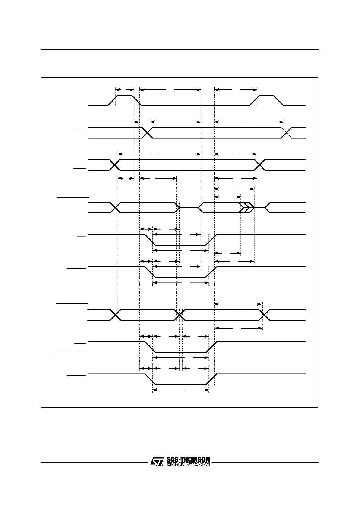
ST10R165
39/53
Figure 14. External Memory Cycle: Multiplexed Bus, No Read/Write Delay, Normal ALE
Data Out
Address
Address
Data In
t
38
Address
ALE
CSx
A23-A16
(A15-A8)
BHE
BUS
Read Cycle
RD
RdCSx
BUS
Write Cycle
WR,
WRL, WRH
WrCSx
t
5
t
16
t
17
t
6
t
7
t
39
t
40
t
25
t
27
t
18
t
19
t
15
t
47
t
13
t
49
t
22
t
23
t
13
t
49
t
9
t
43
t
43
t
9
t
11
t
45
t
11
t
45
t
50
t
51
t
54
t
52
t
56
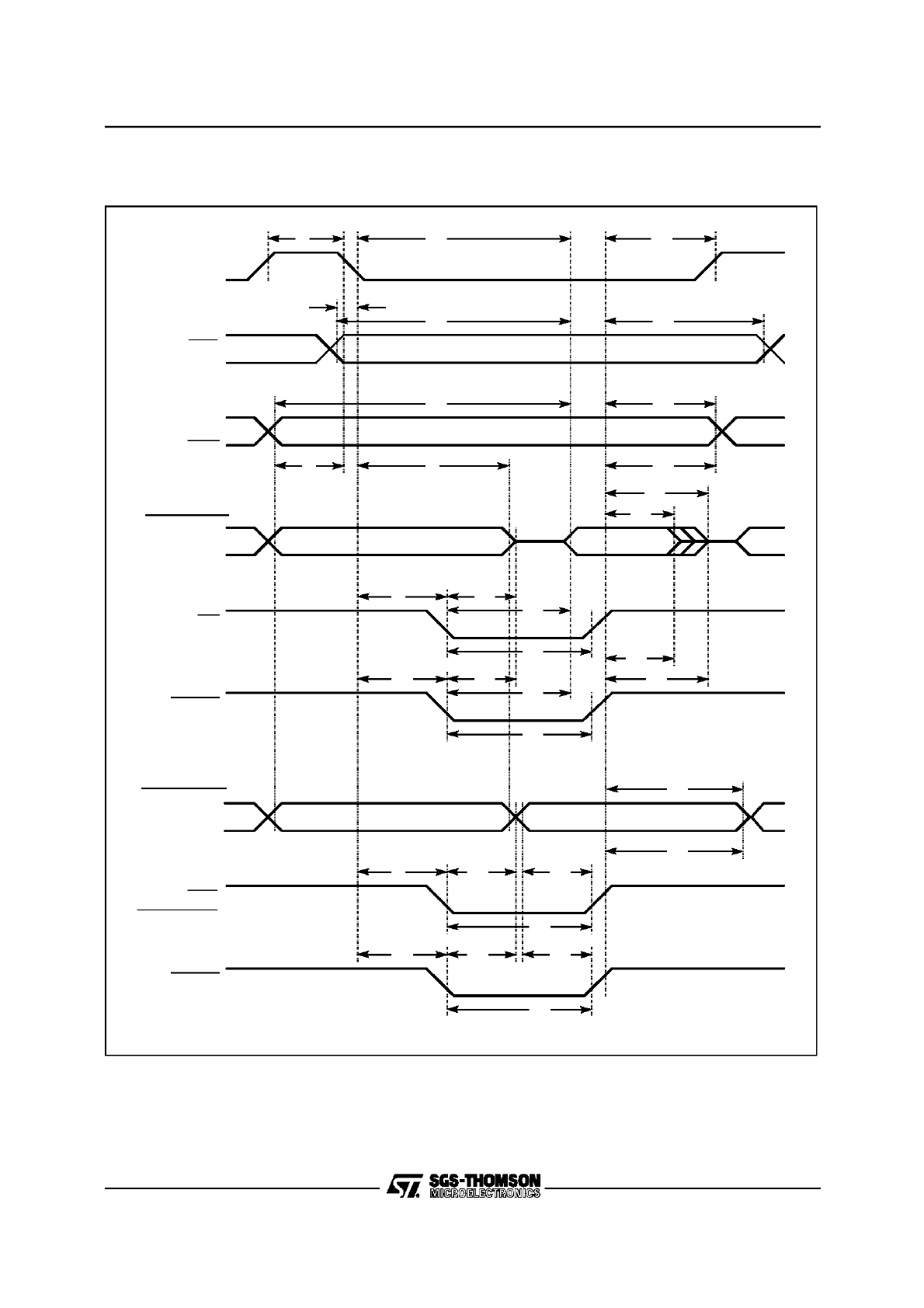
40/53
ST10R165
Figure 15. External Memory Cycle: Multiplexed Bus, No Read/Write Delay, Extended
ALE
Data Out
Address
Data In
Address
t
38
Address
ALE
CSx
A23-A16
(A15-A8)
BHE
BUS
Read Cycle
RD
RdCSx
BUS
Write Cycle
WR,
WRL, WRH
WrCSx
t
5
t
16
t
17
t
6
t
7
t
39
t
40
t
25
t
27
t
18
t
19
t
15
t
47
t
13
t
49
t
22
t
23
t
13
t
49
t
9
t
43
t
43
t
9
t
11
t
45
t
11
t
45
t
50
t
51
t
54
t
52
t
56
ST10R165
41/53
13.5.2.1 Demultiplexed Bus
V
DD
= 5 V
±
10%;
V
SS
= 0 V
T
A
= 0 to +70
°
C
C
L
(for PORT0, PORT1, Port 4, ALE, RD, WR, BHE, CLKOUT) = 100 pF
C
L
(for Port 6, CS) = 100 pF
ALE cycle time = 4 TCL + 2
t
A
+
t
C
+
t
F
(100 ns at 20 MHz CPU clock without waitstates)
Parameter
Symbol
Max. CPU Clock
= 20 MHz
Variable CPU Clock
1/2TCL = 1 to 20 MHz
Unit
min.
max.
min.
max.
ALE high time
t
5
CC
15 +
t
A
–
TCL - 10 +
t
A
–
ns
Address setup to ALE
t
6
CC
10 +
t
A
–
TCL - 15 +
t
A
–
ns
ALE falling edge to RD,
WR (with RW-delay)
t
8
CC
15 +
t
A
–
TCL - 10
+
t
A
–
ns
ALE falling edge to RD,
WR (no RW-delay)
t
9
CC
-10 +
t
A
–
-10
+
t
A
–
ns
RD, WR low time
(with RW-delay)
t
12
CC
40 +
t
C
–
2TCL - 10
+
t
C
–
ns
RD, WR low time
(no RW-delay)
t
13
CC
65 +
t
C
–
3TCL - 10
+
t
C
–
ns
RD to valid data in
(with RW-delay)
t
14
SR
–
30 +
t
C
–
2TCL - 20
+
t
C
ns
RD to valid data in
(no RW-delay)
t
15
SR
–
55 +
t
C
–
3TCL - 20
+
t
C
ns
ALE low to valid data in
t
16
SR
–
55
+
t
A
+
t
C
–
3TCL - 20
+
t
A
+
t
C
ns
Address to valid data in
t
17
SR
–
70
+ 2
t
A
+
t
C
–
4TCL - 30
+ 2
t
A
+
t
C
ns
Data hold after RD
rising edge
t
18
SR
0
–
0
–
ns
Data float after RD rising
edge (with RW-delay)
t
20
SR
–
35 +
t
F
–
2TCL - 15
+
t
F
ns
Data float after RD rising
edge (no RW-delay)
t
21
SR
–
15 +
t
F
–
TCL - 10
+
t
F
ns
Data valid to WR
t
22
CC
35 +
t
C
–
2TCL - 15
+
t
C
–
ns
Data hold after WR
t
24
CC
15 +
t
F
–
TCL - 10 +
t
F
–
ns
ALE rising edge after RD,
WR
t
26
CC
-10 +
t
F
–
-10
+
t
F
–
ns
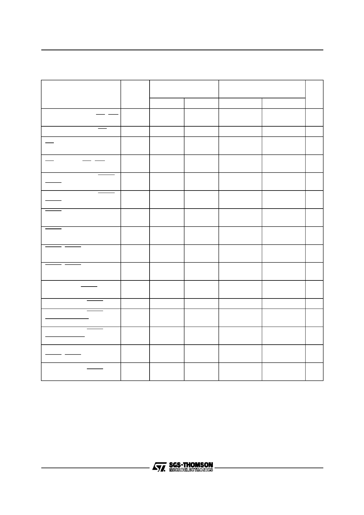
42/53
ST10R165
Address hold after RD, WR
t
28
CC
0 +
t
F
–
0
+
t
F
–
ns
ALE falling edge to CS
t
38
CC
-5 -
t
A
10 -
t
A
-5 -
t
A
10 -
t
A
ns
CS low to Valid Data In
t
39
SR
–
55
+
t
C
+ 2
t
A
–
3TCL - 20
+
t
C
+ 2
t
A
ns
CS hold after RD, WR
t
41
CC
10 +
t
F
–
TCL - 15
+
t
F
–
ns
ALE falling edge to RdCS,
WrCS (with RW-delay)
t
42
CC
20 +
t
A
–
TCL - 5
+
t
A
–
ns
ALE falling edge to RdCS,
WrCS (no RW-delay)
t
43
CC
-5 +
t
A
–
-5
+
t
A
–
ns
RdCS to Valid Data In
(with RW-delay)
t
46
SR
–
25 +
t
C
–
2TCL - 25
+
t
C
ns
RdCS to Valid Data In
(no RW-delay)
t
47
SR
–
50 +
t
C
–
3TCL - 25
+
t
C
ns
RdCS, WrCS Low Time
(with RW-delay)
t
48
CC
40 +
t
C
–
2TCL - 10
+
t
C
–
ns
RdCS, WrCS Low Time
(no RW-delay)
t
49
CC
65 +
t
C
–
3TCL - 10
+
t
C
–
ns
Data valid to WrCS
t
50
CC
35 +
t
C
–
2TCL - 15
+
t
C
–
ns
Data hold after RdCS
t
51
SR
0
–
0
–
ns
Data float after RdCS
(with RW-delay)
t
53
SR
–
30 +
t
F
–
2TCL - 20
+
t
F
ns
Data float after RdCS
(no RW-delay)
t
68
SR
–
5 +
t
F
–
TCL - 20
+
t
F
ns
Address hold after
RdCS, WrCS
t
55
CC
-5 +
t
F
–
-5
+
t
F
–
ns
Data hold after WrCS
t
57
CC
10 +
t
F
–
TCL - 15
+
t
F
–
ns
Parameter
Symbol
Max. CPU Clock
= 20 MHz
Variable CPU Clock
1/2TCL = 1 to 20 MHz
Unit
min.
max.
min.
max.
Demultiplexed Bus (Cont’d)
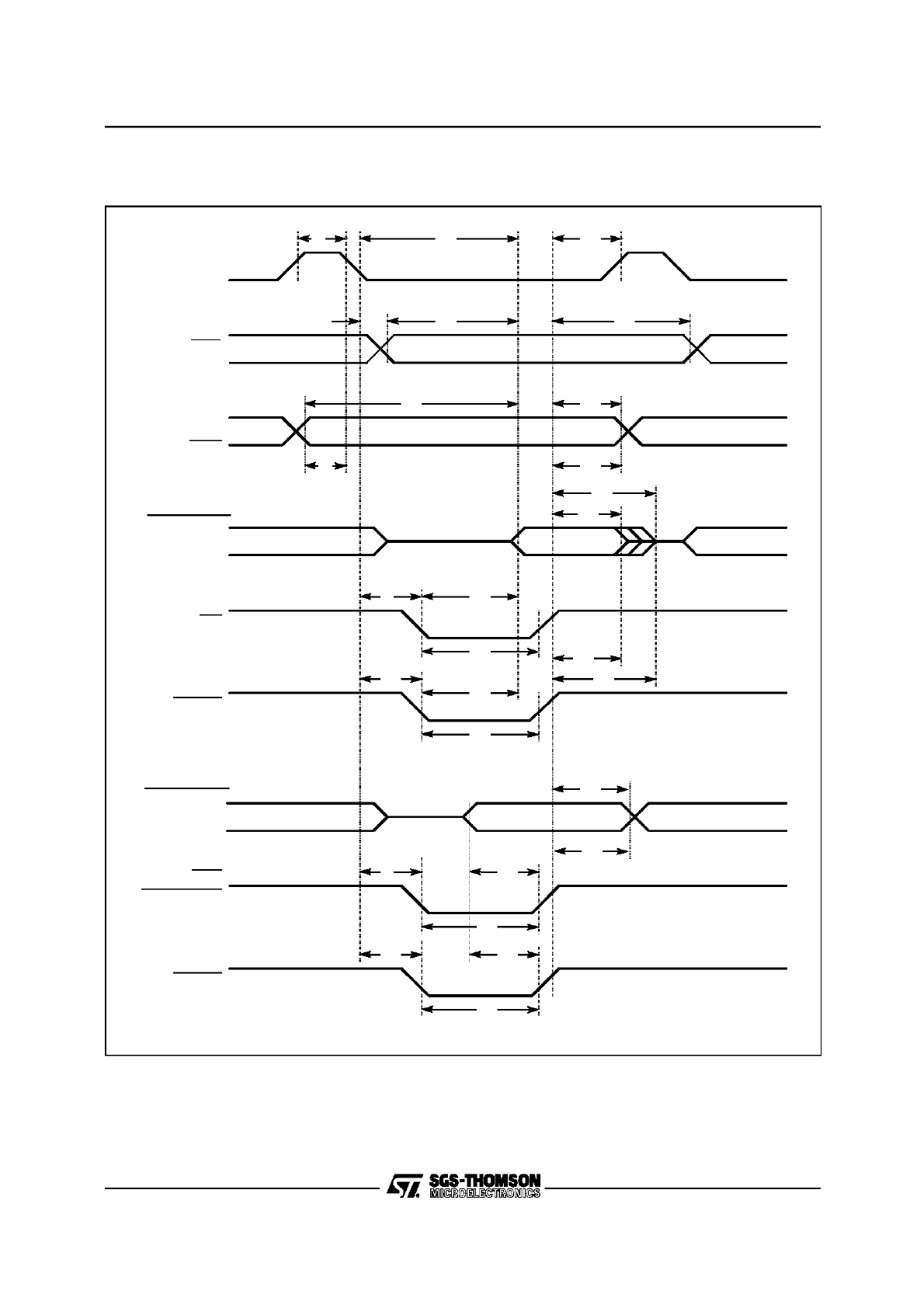
ST10R165
43/53
Figure 16. External Memory Cycle: Demultiplexed Bus, With Read/Write Delay, Normal
ALE
Data Out
Data In
t
38
Address
ALE
CSx
A23-A16
A15-A0
BHE
BUS
(D15-D8)
D7-D0
Read Cycle
RD
RdCSx
Write Cycle
WrCSx
t
5
t
16
t
17
t
6
t
39
t
41
t
26
t
28
t
18
t
20
t
14
t
46
t
12
t
48
t
22
t
24
t
12
t
48
t
8
t
42
t
42
t
8
t
50
t
51
t
55
t
53
t
57
BUS
(D15-D8)
D7-D0
WR,
WRL, WRH
44/53
ST10R165
Figure 17. External Memory Cycle: Demultiplexed Bus, With Read/Write Delay,
Extended ALE
Data Out
Data In
t
38
Address
ALE
CSx
A23-A16
A15-A0
BHE
Read Cycle
RD
RdCSx
Write Cycle
WrCSx
t
5
t
16
t
17
t
6
t
39
t
41
t
26
t
28
t
18
t
20
t
14
t
46
t
12
t
48
t
22
t
24
t
12
t
48
t
8
t
42
t
42
t
8
t
50
t
51
t
55
t
53
t
57
BUS
(D15-D8)
D7-D0
BUS
(D15-D8)
D7-D0
WR,
WRL, WRH
ST10R165
45/53
Figure 18. External Memory Cycle: Demultiplexed Bus, No Read/Write Delay, Normal
ALE
Data Out
Data In
t
38
Address
ALE
CSx
A23-A16
A15-A0
BHE
Read Cycle
RD
RdCSx
Write Cycle
WrCSx
t
5
t
16
t
17
t
6
t
39
t
41
t
26
t
28
t
18
t
21
t
15
t
47
t
13
t
49
t
22
t
24
t
13
t
49
t
9
t
43
t
43
t
9
t
50
t
51
t
55
t
68
t
57
BUS
(D15-D8)
D7-D0
BUS
(D15-D8)
D7-D0
WR,
WRL, WRH
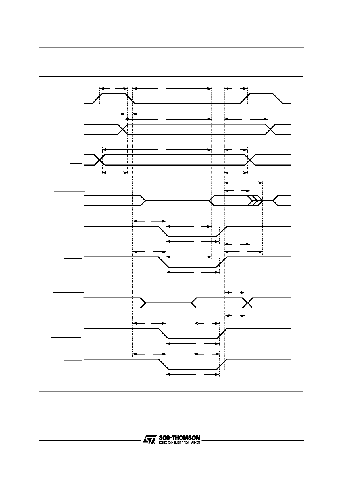
46/53
ST10R165
Figure 19. External Memory Cycle: Demultiplexed Bus, No Read/Write Delay, Extended
ALE
Data Out
Data In
t
38
Address
ALE
CSx
A23-A16
A15-A0
BHE
Read Cycle
RD
RdCSx
Write Cycle
WR,
WRL, WRH
WrCSx
t
5
t
16
t
17
t
6
t
39
t
41
t
26
t
28
t
18
t
21
t
15
t
47
t
13
t
49
t
22
t
24
t
13
t
49
t
9
t
43
t
43
t
9
t
50
t
51
t
55
t
68
t
57
BUS
(D15-D8)
D7-D0
BUS
(D15-D8)
D7-D0
ST10R165
47/53
AC Characteristics (Cont’d)
CLKOUT and READY
V
DD
= 5 V
±
10%;
V
SS
= 0 V
T
A
= 0 to +70
°
C
C
L
(for PORT0, PORT1, Port 4, ALE, RD, WR, BHE, CLKOUT) = 100 pF
C
L
(for Port 6, CS) = 100 pF
Notes:
1)
These timings are given for test purposes only, in order to assure recognition at a
specific clock edge.
2)
Demultiplexed bus is the worst case. For multiplexed bus 2TCL are to be added to
the maximum values. This adds even more time for deactivating READY.
The 2t
A
refer to the next following bus cycle.
Parameter
Symbol
Max. CPU Clock
= 20 MHz
Variable CPU Clock
1/2TCL = 1 to 20 MHz
Unit
min.
max.
min.
max.
CLKOUT cycle time
t
29
CC
50
50
2TCL
2TCL
ns
CLKOUT high time
t
30
CC
20
–
TCL – 5
–
ns
CLKOUT low time
t
31
CC
15
–
TCL – 10
–
ns
CLKOUT rise time
t
32
CC
–
5
–
5
ns
CLKOUT fall time
t
33
CC
–
5
–
5
ns
CLKOUT rising edge to
ALE falling edge
t
34
CC
0 +
t
A
10 +
t
A
0 +
t
A
10 +
t
A
ns
Synchronous READY
setup time to CLKOUT
t
35
SR
10
–
10
–
ns
Synchronous READY
hold time after CLKOUT
t
36
SR
0
–
0
–
ns
Asynchronous READY
low time
t
37
SR
65
–
2TCL + 15
–
ns
Asynchronous READY
setup time
1)
t
58
SR
15
–
15
–
ns
Asynchronous READY
hold time
1)
t
59
SR
0
–
0
–
ns
Async. READY hold time
after RD, WR high (Demul-
tiplexed Bus)
2)
t
60
SR
0
0
+ 2
t
A
+
t
F
2)
0
TCL - 25
+ 2
t
A
+
t
F
2)
ns
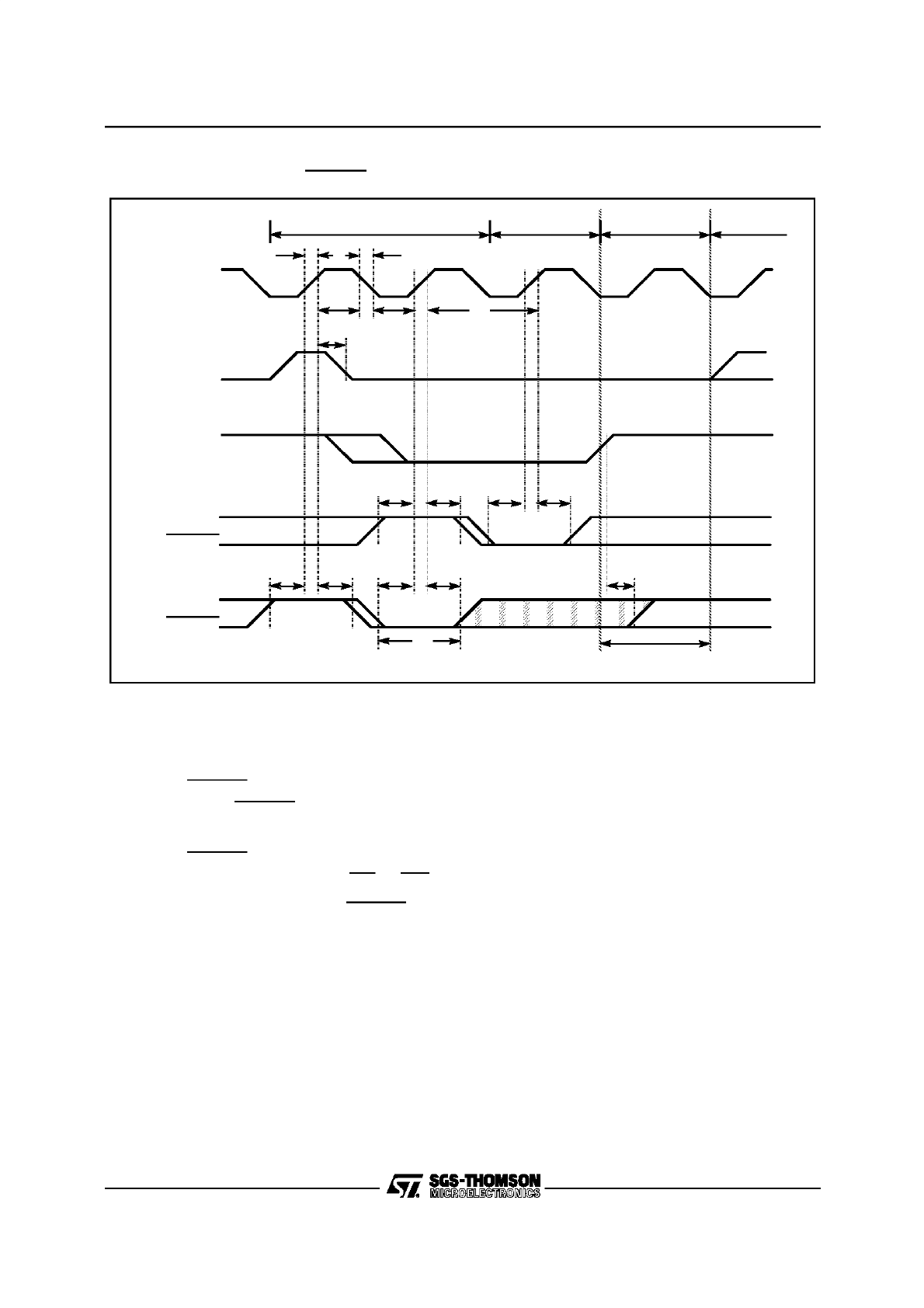
48/53
ST10R165
Figure 20. CLKOUT and READY
Notes:
1)
Cycle as programmed, including MCTC waitstates (Example shows 0 MCTC WS).
2)
The leading edge of the respective command depends on RW-delay.
3)
READY sampled HIGH at this sampling point generates a READY controlled wait-
state, READY sampled LOW at this sampling point terminates the currently run-
ning bus cycle.
4)
READY may be deactivated in response to the trailing (rising) edge of the corre-
sponding command (RD or WR).
5)
If the Asynchronous READY signal does not fulfill the indicated setup and hold
times with respect to CLKOUT (e.g. because CLKOUT is not enabled), it must ful-
fill
t
37
in order to be safely synchronized. This is guaranteed, if READY is removed
in response to the command (see Note 4)).
6)
Multiplexed bus modes have a MUX waitstate added after a bus cycle, and an
additional MTTC waitstate may be inserted here.
For a multiplexed bus with MTTC waitstate this delay is 2 CLKOUT cycles, for a
demultiplexed bus without MTTC waitstate this delay is zero.
7)
The next external bus cycle may start here.
CLKOUT
ALE
t
30
t
34
Sync
READY
t
35
t
36
t
35
t
36
Async
READY
t
58
t
59
t
58
t
59
waitstate
READY
MUX/Tristate 6)
t
32
t
33
t
29
Running cycle 1)
t
31
t
37
3)
3)
5)
Command RD,
WR
t
60
4)
see 6)
2)
7)
3)
3)
ST10R165
49/53
13.5.2.2 External Bus Arbitration
V
DD
= 5 V
±
10%;
V
SS
= 0 V
T
A
= 0 to +70
°
C
C
L
(for PORT0, PORT1, Port 4, ALE, RD, WR, BHE, CLKOUT) = 100 pF
C
L
(for Port 6, CS) = 100 pF
Parameter
Symbol
Max. CPU Clock
= 20 MHz
Variable CPU Clock
1/2TCL = 1 to 20 MHz
Unit
min.
max.
min.
max.
HOLD input setup time
to CLKOUT
t
61
SR
20
–
20
–
ns
CLKOUT to HLDA high
or BREQ low delay
t
62
CC
–
20
–
20
ns
CLKOUT to HLDA low
or BREQ high delay
t
63
CC
–
20
–
20
ns
CSx release
t
64
CC
–
20
–
20
ns
CSx drive
t
65
CC
-5
25
-5
25
ns
Other signals release
t
66
CC
–
20
–
20
ns
Other signals drive
t
67
CC
-5
25
-5
25
ns
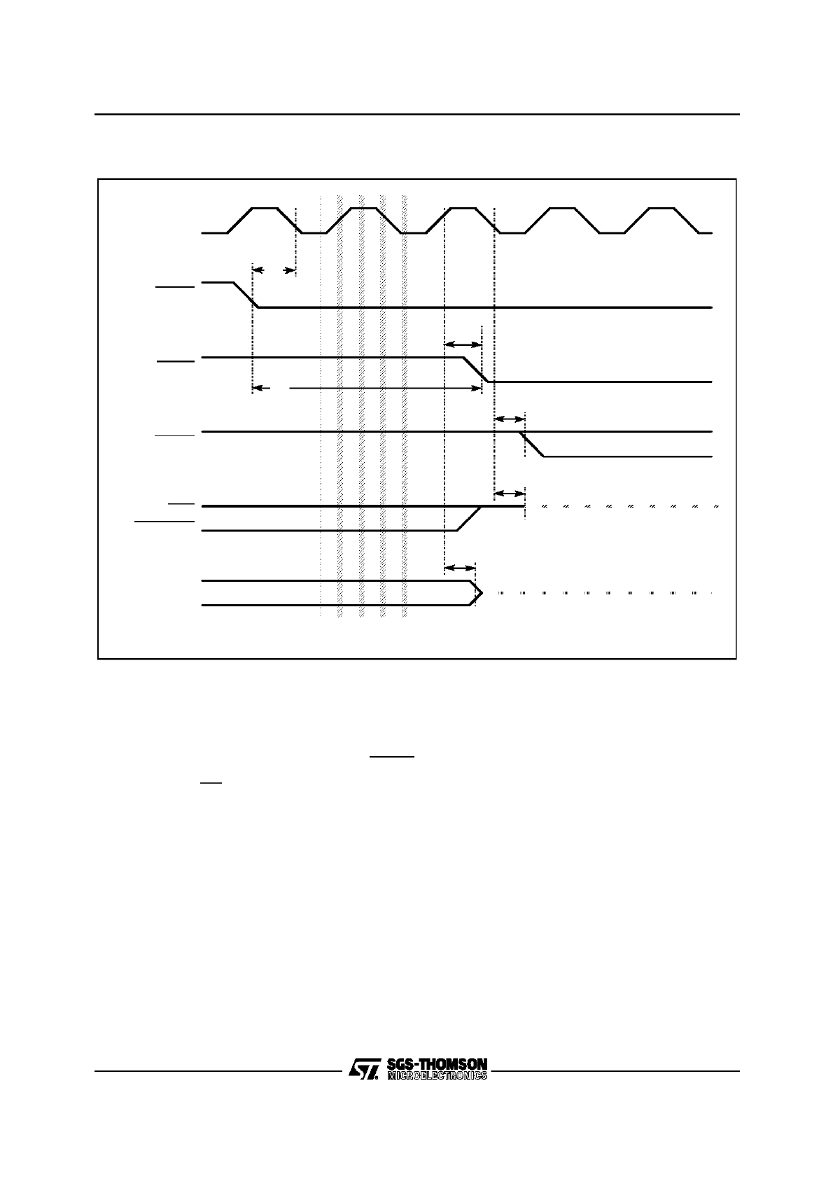
50/53
ST10R165
Figure 21. External Bus Arbitration, Releasing the Bus
Notes:
1)
The ST10R165 will complete the currently running bus cycle before granting bus
access.
2)
This is the first possibility for BREQ to get active.
3)
The CS outputs will be resistive high (pullup) after
t
64
.
CLKOUT
HOLD
t
61
HLDA
t
63
Other
Signals
t
66
1)
CSx
(On P6.x)
t
64
1)
2)
BREQ
t
62
3)
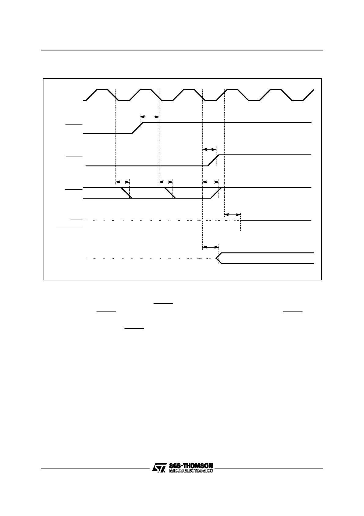
ST10R165
51/53
Figure 22. External Bus Arbitration, (Regaining the Bus)
Notes:
1)
This is the last chance for BREQ to trigger the indicated regain-sequence.
Even if BREQ is activated earlier, the regain-sequence is initiated by HOLD going
high.
Please note that HOLD may also be deactivated without the ST10R165 requesting
the bus.
2)
The next ST10R165 driven bus cycle may start here.
CLKOUT
HOLD
HLDA
Other
Signals
t
62
CSx
(On P6.x)
t
67
t
62
1)
2)
t
65
t
61
BREQ
t
63
t
62
52/53
ST10R165
14 PACKAGE MECHANICAL DATA
Figure 23. Package Outline PQFP100 (14 x 20 mm)
Figure 24. Package Outline TQFP100 (14 x 14 mm)
Dim
mm
inches
Min
Typ
Max
Min
Typ
Max
A
3.30
0.134
A2
2.55
2.80
3.05
0.100
0.110
0.120
D
22.9
23.2
22.45
0.904
0.913
0.923
D1
19.9
20.0
20.10
0.783
0.787
0.791
D3
18.8
0.742
E
16.9
17.2
17.45
0.667
0.677
0.687
E1
13.9
14.0
14.10
0.547
0.551
0.555
E3
12.3
0.486
e
0.65
0.026
Number of Pins
ND
30
NE
20
N
100
Dim
mm
inches
Min
Typ
Max
Min
Typ
Max
A
1.60
0.063
A2
1.35
1.40
1.45
0.053
0.055
0.057
D
15.7
16.0
16.25
0.620
0.630
0.640
D1
13.9
14.0
14.10
0.547
0.551
0.555
D3
12.0
0.472
E
15.7
16.0
16.25
0.620
0.630
0.640
E1
13.9
14.0
14.10
0.547
0.551
0.555
E3
12.0
0.472
e
0.50
0.020
Number of Pins
ND
25
NE
25
N
100

ST10R165
53/53
15 ORDERING INFORMATION
Information furnished is believed to be accurate and reliable. However, SGS-THOMSO N Microelectronics assumes no
responsibility for the consequences of use of such information nor for any infringement of patents or other rights of third parties
which may result from its use. No license is granted by implication or otherwise under any patent or patent rights of SGS-
THOMSON Microelectronics. Specification mentioned in this publication are subject to change without notice. This publication
supersedes and replaces all information previously supplied.
SGS-THOMSON Microelectronics products are not authorized for use as critical components in life support devices or systems
without express written approval of SGS-THOM SON Microelectronics.
19
95 SGS-THOMSON Microelectronics -Printed in Italy - All Rights Reserved.
SGS-THOMSON Microelectronics GROUP OF COMPANI ES
Australia - Brazil - China - France - Germany - Hong Kong - Italy - Japan - Korea - Malaysia - Malta - Morocco - The Netherlands
- Singapore - Spain - Sweden - Switzerland - Taiwan - Thailand - United Kingdom - U.S.A.
Salestype
Temperature range
Package
ST10R165
BQ1
0
°
C to 70
°
C
PQFP100(14x 20)
ST10R165
BQ6
- 40
°
C to 85
°
C
PQFP100(14x 20)
ST10R165
BT1
0
°
C to 70
°
C
TQFP100(14x 14)
ST10R165
BT6
- 40
°
C to 85
°
C
TQFP100(14x 14)