

C167 FAMILY
PRELIMINARY
USER MANUAL

C167 FAMILY PRELIMINARY USER MANUAL
2/180
USE IN LIFE SUPPORT DEVICES OR SYSTEMS MUST BE EXPRESSLY AUTHORIZED
SGS-THOMSON PRODUCTS ARE NOT AUTHORIZED FOR USE AS CRITICAL COMPONENTS IN LIFE
SUPPORT DEVICES OR SYSTEMS WITHOUT THE EXPRESS WRITTEN APPROVAL OF SGS-THOMSON
Microelectronics.
As used herein:
1. Life support devices or systems are those which
(a) are intended for surgical implant into the body,
or (b) support or sustain life, and whose failure to
perform, when properly used in accordance with
instructions for use provided with the product, can
be reasonably expected to result in significant
injury to the user.
2. A critical component is any component of a life
support device or system whose failure to perform
can reasonably be expected to cause the failure of
the life support device or system, or to affect its
safety or effectiveness.

C167 FAMILY PRELIMINARY USER MANUAL
3/180
TABLE OF CONTENTS
TABLE OF CONTENTS ................................ ......................... ....... ..............................
3
ST10167......................... ....... ............................. ..........................................................
5
1. Instruction Set................................................................................................ ........
7
1.1 Atomic Instruction............................ .................................................................7
1.2 Extend Segment/Extend Page Instructions .................................................... 8
1.3 Extend Register Instructions...........................................................................8
2. On-Chip Memory ......................... ....... ............................. ...................................
23
2.1 On-Chip ROM ...............................................................................................23
2.2 On-Chip RAM............................ ....................................................................24
2.3 PEC Pointer Address Space............................. ............................................26
2.4 Extended Special Function Register Space (ESFR)......................... ....... .....26
2.5 Internal Address Space.................................................................................29
3. Bus Control Unit......................... ....... ............................. ....................................
31
3.1 Extended Address Space ........................ ........ ............................ .................
31
3.2 System and Bus Configuration Control............................... ..........................33
3.2.1
SYSCON Register...............................................................................33
3.2.2
BUSCON0 Register................................ .......................... ...................
36
3.2.3
BUSCON1..4 and ADDRSEL1..4 Registers........................................ 38
3.3 Chip Selects ................................................................ ........................ ........ ..
43
3.3.1
Address Chip Selects ............................. .............................................44
3.3.2
Read/Write Chip Selects......................................................................45
3.4 Byte High Enable or Write High , Write Low Operation......................... ....... .47
3.5 System Startup Configuration................................................................ .......51
3.6 On-Chip Bootstrap Loader............................................................................ 58
4. PWM Module................................................................................................ .......
61
4.1 PWM-Channel.............................. .................................................................62
4.1.1
Operating Modes................................ ........................ ........ .................
63
4.1.2
PWM Module Registers.......................... .................................... .........
71
4.1.3
Interrupt Request Generation.............................................................. 76
4.1.4
PWM Output Signals ................................................................ ...........
78
5. Second Capture/Compare Unit, CAPCOM2 .....................................................79
6. Asynchronous/Synchronous Serial Interface................................................. 87
6.1 Even / Odd Parity Selection.............................. ............................................87
6.2 Double Buffered Transmit ............................. ................................................88
7. Synchronous Serial Channel, SSC........................ ........ ............................ .......
91
7.1 SSC Block Diagram ................................................................ ......................
91
7.2 General Operation of the SSC ......................................................................93
7.3 SSC Control, Status and Data Registers...................................................... 94

C167 FAMILY PRELIMINARY USER MANUAL
4/180
7.3.1
SSC Control Register SSCCON.......................... ................................94
7.3.2
Buffer Registers SSCTB and SSCRB ................................ ...............100
7.3.3
Baud Rate Register SSCBR................................ ..............................100
7.3.4
Interrupt Control Registers ................................................................101
7.3.5
Port Control Registers .......................................................................103
7.4 Detailled Operation of the SSC ...................................................................105
7.4.1
Single Master, Full-Duplex Operation................................................ 106
7.4.2
Multi-Master, Full-Duplex Operation.................................................. 109
7.4.3
Half-Duplex Operation....................................................................... 110
7.4.4
Continuous Transfers ........................... .................................... .........
112
7.5 Error Detection................................................................ ............................ 113
7.5.1
Receive Error (Master and Slave Mode)........................................... 114
7.5.2
Phase Error (Master and Slave Mode)................................ ..............114
7.5.3
Baud Rate Error (Slave Mode).......................................................... 115
7.5.4
Transmit Error (Slave Mode)............................................................. 115
8. A/D Converter (ADC) ........................................................................................117
8.1 Additional A/D Input Channels ........................ ........ ............................ ........117
8.2 Wait for ADDAT Read Mode........................... .................................... ........
118
8.3 Channel Injection Mode ............................... ...............................................122
9. GPT1 and GPT2 Enhancements ............................... ......................................127
10. Interrupt System...............................................................................................133
10.1 External Interrupts................................................................ ..................... 133
10.2 Additional Peripheral Interrupts................................ ........................... ......134
11. Ports ................................................................................................ ..................
137
11.0 PORT0: Ports P0L and P0H ....................................................................141
11.1 PORT1: Ports P1L and P1H ....................................................................144
11.2 PORT2 ................................ ........................ ........ ........................... ...........
146
11.3 PORT3 ................................ ........................ ........ ............................ ..........
148
11.4 PORT4 ................................ ........................ ........ ............................ ..........
151
11.5 PORT5 ................................ ........................ ........ ............................ ..........
153
11.6 PORT6 ................................ ........................ ........ ............................ ..........
154
11.7 PORT7 ................................ ........................ ........ ............................ ..........
159
11.8 PORT8 ................................ ........................ ........ ............................ ..........
163
12. Dedicated Pins................... ............................................. ........................... .......
167
13. Pinout ................................................................................................................169
14. Index (figures) ............................ ......................................................................179

C167 FAMILY PRELIMINARY USER MANUAL
5/180
ST10167
This Preliminary User Manual describes the enhancements bring to the new ST10
Family, the C167 Family and specially the ST10167 which is the first derivative
component of the C167 Family. Compared to the ST10x166, besides adding more
functionality in the peripheral and bus controller section, some enhancements and
changes are made in the CPU core of the C167. The following list gives a short
overview on the additional features and functions of the ST10167:
-
8 KByte On-Chip Mask-Programmable ROM
-
2 KByte On-Chip RAM
Extended System Stack, Variable, and Register Bank Space
PEC Pointers Mapped to Non-Bitaddressable Space
-
Additional Instructions to Support HLL and Operating Systems
-
Extended Address Range up to 16 MByte
-
Five Bus Configuration Registers
-
Five Selectable Chip Select Signals
-
Extended SFR Space
-
Enhanced A/D Converter Operation:
16 Analog Input Channels
Wait for Read Mode: Start New Conversion after ADDAT Read
Channel Injection: Convert Specific Channel during Auto Scan or
Continuous Mode
-
Second Capture/Compare Unit with 16 Channels
-
Serial Interfaces:
One Synchronous/Asynchronous Serial Interface (ASC0) with Even/Odd
Parity Selection
One Synchronous Serial Interface (SSC) with Master/Slave Option
-
Pulse Width Modulation (PWM) Unit with 4 Independent Channels:
Up to 78 KHz Frequency with 8-Bit Resolution
Four Modes of Operation: Standard, Symetrical, Burst Mode, Single Shot
-
Extended Interrupt System:
8 Fast External Interrupt Inputs, 50 ns Sample Rate
24 Additional Interrupt Sources and Vectors
-
On-Chip Bootstrap Loader
-
144-Pin MQFP Package (EIAJ)

C167 FAMILY PRELIMINARY USER MANUAL
6/180
In this document, only these add-on features and differences of the C167 compared
to the ST10x166 are described. For more detailled information about features and
functions of the ST10 family please refer to the ST10 User Manual.
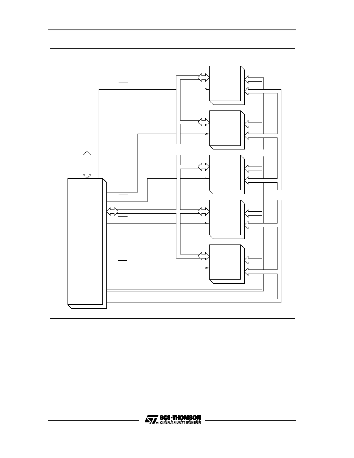
Figure 1. Block diagram of the major units of the ST10167
VR001925
CPU
CORE
RAM
ROM
OSC
Interrupt Controller
WDT
P0
P1
P8
P7
GPT2
GPT1
ADC
ASC
SSC
PWM
PEC
BUS
CTL
CAPCOM2
CAPCOM1
P4
P6
P2
P3
P5

C167 FAMILY PRELIMINARY USER MANUAL
7/180
1. INSTRUCTION SET
The instruction set of the C167 is enhanced by a number of instructions, which can
greatly reduce the code size generated by C-Compilers, and which enable the user
to write uninterruptable instruction sequences in a very effective way. A further
instruction is used to support the Extended SFR space in the C167 (see Chapter
2.4). The new instructions are described below, the syntax and formats of these
instructions are detailled on the next pages.
1.1 Atomic Instruction
This instruction is intended to allow the user to write an uninterruptable sequence of
code. The execution of this instruction causes the interrupt system (standard
interrupts and PEC requests) and Class A Traps to be disabled for a specific
number of instructions, between 1 to 4 instructions. All instructions requiring multiple
cycles or hold states are regarded as one instruction in this sense (e.g. MUL is one
instruction). The atomic instruction is immediately active such that no NOPs are
required. Any instruction type can be used with this instruction.
Note that, while Class A Traps (NMI#, Stack Overflow/Underflow) are disabled during
the scope of the atomic instruction, the occurence of a Class B Trap (Illegal Opcode,
Illegal Bus Access, etc.) will interrupt the atomic sequence, since it indicates a
severe hardware problem.
The operation of the atomic instruction is the basis also for the Extend instructions.
Example:
ATOMIC #3
; scope is 3 instructions
; the following 3 instructions are uninterruptable
MOV
R0,#1234h
; instr. 1
MOV
R1,#5678h
; instr. 2
MUL
R0,R1
; instr. 3: MUL regarded as one instruction
MOV
R2,MDL
; this instruction is out of the scope of the atomic sequence

C167 FAMILY PRELIMINARY USER MANUAL
8/180
1.2
Extend Segment/Extend Page Instructions
These instructions allow the user to bypass the code segment and data page
scheme for a specific number of instructions (between 1 to 4). These instructions will
mainly be used by HLL-Compilers to access large data areas without the overhead of
data page pointer swapping. As with the atomic instruction, interrupts and Class A
Traps are disabled for up to 4 instructions after the extend instructions. Additional
instruction formats are implemented for a combination of the Extend Segment/Extend
Page instructions with the Extend Register instruction.
1.3
Extend Register Instructions
In the C167, due to the amount of Special Function Registers (SFRs) required to
control the on-chip peripherals, the SFR space is extended. This new Extended SFR
range, ESFR, can be accessed like any other memory location with a 16-bit address
(mem or [Rw]). However, when using short 8-bit addresses (REG or BITOFF), a
distinction has to be made between the normal and the extended SFR space (see
also Chapter 2.4). For this purpose, Extend Register instructions are implemented,
which allow access to the ESFR space with short 8-bit addresses for a specific
number of instructions (between 1 and 4). Again, interrupts and Class A Traps are
disabled during execution of this code sequence. Additional instruction formats are
implemented for a combination of the Extend Register instruction with the Extend
Segment/Extend Page instructions. Examples for these instructions can be found in
section 2.4.

C167 FAMILY PRELIMINARY USER MANUAL
9/180
Note:
Signal active low will be marked in the text with # and with
__
in the
figures.

C167 FAMILY PRELIMINARY USER MANUAL
10/180
ATOMIC
begin ATOMIC sequence
ATOMIC
op1
OPERATION
(count) <= op1(1 <=
op1 <= 4)
Disable Interrupts and Class A Traps
DO WHILE (count != 0 AND Class B Trap Condition != TRUE)
next instruction
(count) <= (count) - 1
END WHILE
(count) = 0
Enable Interrupts and Traps
Causes standard and PEC interrupts and class A hardware
traps to be disabled for a specified number of instructions. The
ATOMIC instruction becomes immediately active such that no
additional NOPs are required.
Depending on the value of op1, the period of validity of the
ATOMIC sequence extends over the sequence of the next 1 to
4 instructions being executed after the ATOMIC instruction. All
instructions requiring multiple cycles or hold states to be
executed are regarded as one instruction in this sense. Any
instruction type can be used with the ATOMIC instruction.
NOTE: A lot of care must be taken over the use of the ATOMIC
instruction with other system control or branch instructions. One
must also be very careful when a class B trap condition
becomes present before the ATOMIC instruction sequence is
completed. In such a case, the ATOMIC instruction ceases its
validity, the interrupt locking is removed, and the class B trap is
executed. An ATOMIC instruction sequence can normally not
be continued properly if it was interrupted!

C167 FAMILY PRELIMINARY USER MANUAL
11/180
ATOMIC
begin ATOMIC sequence
FLAGS
E
Z
V
C
N
-
-
-
-
-
E
Not affected
Z
Not affected
V
Not affected
C
Not affected
N
Not affected
INSTRUCTION FORMAT
Mnemonic
Operands
Format
Bytes
ATOMIC
#data2
D1 :00##-0
2

C167 FAMILY PRELIMINARY USER MANUAL
12/180
EXTR
begin EXTended Register sequence
EXTR
op1
OPERATION
(count) <= op1(1 <= op1 <= 4)
Disable Interrupts and Class A Traps
SFR range = Extended
DO WHILE (count != 0 AND Class B Trap Condition != TRUE)
next instruction
(count) <= (count) - 1
END WHILE
(count) = 0
SFR range = Standard
Enable Interrupts and Traps
Causes all SFR or SFR bit accesses via the ’reg’, ’bitoff’ or
’bitaddr’ addressing modes being made to the Extended SFR
space for a specified number of instructions. During their
execution, both standard and PEC interrupts and class A
hardware traps are locked. The EXTR instruction becomes
immediately active such that no additional NOPs are required.
Depending on the value of op1, the period of validity of the
EXTR instruction extends over the sequence of the next 1 to 4
instructions being executed after the EXTR instruction. All
instructions requiring multiple cycles or hold states to be
executed are regarded as one instruction in this sense. Any
instruction type can be used with the EXTR instruction.
NOTE: A lot of care must be taken over the use of the EXTR
instruction with other system control or branch instructions. One
must also be very careful when a class B trap condition
becomes present before the EXTR instruction sequence is
completed. In such a case, the EXTR instruction ceases its
validity, the interrupt locking is removed, and the class B trap is
executed. An EXTR instruction sequence can normally not be
continued properly if it was interrupted!

C167 FAMILY PRELIMINARY USER MANUAL
13/180
EXTR
begin EXTended Register sequence
FLAGS
E
Z
V
C
N
-
-
-
-
-
E
Not affected
Z
Not affected
V
Not affected
C
Not affected
N
Not affected
INSTRUCTION FORMAT
Mnemonic
Operands
Format
Bytes
EXTR
#data2
D1 :10##-0
2

C167 FAMILY PRELIMINARY USER MANUAL
14/180
EXTP
begin EXTended Page sequence
EXTP
op1, op2
OPERATION
(count) <= op2(1 <= op2 <= 4)
Disable Interrupts and Class A Traps
Data Page = (op1)
DO WHILE (count != 0 AND Class B Trap Condition != TRUE)
next instruction
(count) <= (count) - 1
END WHILE
(count) = 0
Data Page = (DPPx)
Enable Interrupts and Traps
Overrides the standard DPP addressing scheme of the long
and indirect addressing modes for a specified number of
instructions. During their execution, both standard and PEC
interrupts and class A hardware traps are locked. The EXTP
instruction becomes immediately active such that no additional
NOPs are required.
For any long (’mem’) or indirect ([...]) address in the EXTP
instruction sequence, the 10-bit page number (address bits
A
23
-A
14
) is not determined by the contents of a DPP register
but by the value of op1 itself. The 14-bit page offset (address
bits A
13
-A
0
) is derived from the long or indirect address as
usual.
Depending on the value of op2, the period of validity of the
EXTP instruction extends over the sequence of the next 1 to 4
instructions being executed after the EXTP instruction. All
instructions requiring multiple cycles or hold states to be
executed are regarded as one instruction in this sense. Any
instruction type can be used with the EXTP instruction.

C167 FAMILY PRELIMINARY USER MANUAL
15/180
EXTP
begin EXTended Page sequence
NOTE: A lot of care must be taken over the use of the EXTP
instruction with other system control or branch instructions. One
must also be very careful when a class B trap condition
becomes present before the EXTP instruction sequence is
completed. In such a case, the EXTP instruction ceases its
validity, the interrupt locking is removed, and the class B trap is
executed. An EXTP instruction sequence can normally not be
continued properly if it was interrupted!
FLAGS
E
Z
V
C
N
-
-
-
-
-
E
Not affected
Z
Not affected
V
Not affected
C
Not affected
N
Not affected
INSTRUCTION FORMAT
Mnemonic
Operands
Format
Bytes
EXTP
Rwm, #data2
DC :01##-m
2
EXTP
#pag,#data2
D7 :01##-0 pp 0:00pp
4

C167 FAMILY PRELIMINARY USER MANUAL
16/180
EXTPR
begin EXTended Page and Register sequence
EXTPR
op1, op2
OPERATION
(count) <= op2(1 <= op2 <= 4)
Disable Interrupts and Class A Traps
Data Page = (op1) AND SFR range = Extended
DO WHILE (count != 0 AND Class B Trap Condition != TRUE)
next instruction
(count) <= (count) - 1
END WHILE
(count) = 0
Data Page = (DPPx) AND SFR range = Standard
Enable Interrupts and Traps
Overrides the standard DPP addressing scheme of the long
and indirect addressing modes and causes all SFR or SFR bit
accesses via the ’reg’, ’bitoff’ or ’bitaddr’ addressing modes
being made to the Extended SFR space for a specified number
of instructions. During their execution, both standard and PEC
interrupts and class A hardware traps are locked. The EXTPR
instruction becomes immediately active such that no additional
NOPs are required.
For any long (’mem’) or indirect ([...]) address in the EXTPR
instruction sequence, the 10-bit page number (address bits
A
23
-A
14
) is not determined by the contents of a DPP register
but by the value of op1 itself. The 14-bit page offset (address
bits A
13
-A
0
) is derived from the long or indirect address as
usual.
Depending on the value of op2, the period of validity of the
EXTPR instruction extends over the sequence of the next 1 to 4
instructions being executed after the EXTPR instruction. All
instructions requiring multiple cycles or hold states to be
executed are regarded as one instruction in this sense. Any
instruction type can be used with the EXTPR instruction.

C167 FAMILY PRELIMINARY USER MANUAL
17/180
EXTPR
begin EXTended Page and Register sequence
NOTE: A lot of care must be taken over the use of the EXTPR
instruction with other system control or branch instructions. One
must also be very careful when a class B trap condition
becomes present before the EXTPR instruction sequence is
completed. In such a case, the EXTPR instruction ceases its
validity, the interrupt locking is removed, and the class B trap is
executed. An EXTPR instruction sequence can normally not be
continued properly if it was interrupted!
FLAGS
E
Z
V
C
N
-
-
-
-
-
E
Not affected
Z
Not affected
V
Not affected
C
Not affected
N
Not affected
INSTRUCTION FORMAT
Mnemonic
Operands
Format
Bytes
EXTPR
Rwm, #data2
DC :11##-m
2
EXTPR
#pag,#data2
D7 :11##-0 pp 0:00pp
4

C167 FAMILY PRELIMINARY USER MANUAL
18/180
EXTS
begin EXTended Segment sequence
EXTS
op1, op2
OPERATION
(count) <= op2(1 <= op2 <= 4)
Disable Interrupts and Class A Traps
Data Segment = (op1)
DO WHILE (count != 0 AND Class B Trap Condition != TRUE)
next instruction
(count) <= (count) - 1
END WHILE
(count) = 0
Data Page= (DPPx)
Enable Interrupts and Traps
Overrides the standard DPP addressing scheme of the long
and indirect addressing modes for a specified number of
instructions. During their execution, both standard and PEC
interrupts and class A hardware traps are locked. The EXTS
instruction becomes immediately active such that no additional
NOPs are required.
For any long (’mem’) or indirect ([...]) address in an EXTS
instruction sequence, the value of op1 determines the 8-bit
segment (address bits A
23
-A
16
) valid for the corresponding
data access. The long or indirect address itself represents the
16-bit segment offset (address bits A
15
-A
0
).
Depending on the value of op2, the period of validity of the
EXTS instruction extends over the sequence of the next 1 to 4
instructions being executed after the EXTS instruction. All
instructions requiring multiple cycles or hold states to be
executed are regarded as one instruction in this sense. Any
instruction type can be used with the EXTS instruction.

C167 FAMILY PRELIMINARY USER MANUAL
19/180
EXTS
begin EXTended Segment sequence
NOTE: A lot of care must be taken over the use of the EXTS
instruction with other system control or branch instructions. One
must also be very careful when a class B trap condition
becomes present before the EXTS instruction sequence is
completed. In such a case, the EXTS instruction ceases its
validity, the interrupt locking is removed, and the class B trap is
executed. An EXTS instruction sequence can normally not be
continued properly if it was interrupted!
FLAGS
E
Z
V
C
N
-
-
-
-
-
E
Not affected
Z
Not affected
V
Not affected
C
Not affected
N
Not affected
INSTRUCTION FORMAT
Mnemonic
Operands
Format
Bytes
EXTS
Rwm, #data2
DC :00##-m
2
EXTS
#seg,#data2
D7 :00##-0 ss 00
4

C167 FAMILY PRELIMINARY USER MANUAL
20/180
EXTSR
begin EXTended Segment and Register sequence
EXTSR
op1, op2
OPERATION
(count) <= op1(1 <= op2 <= 4)
Disable Interrupts and Class A Traps
Data Segment = (op1) AND SFR range = Extended
DO WHILE (count
!=
0 AND Class B Trap Condition != TRUE)
next instruction
(count) <= (count) - 1
END WHILE
(count) = 0
Data Page= (DPPx) AND SFR range = Standard
Enable Interrupts and Traps
Overrides the standard DPP addressing scheme of the long
and indirect addressing modes and causes all SFR or SFR bit
accesses via the ’reg’, ’bitoff’ or ’bitaddr’ addressing modes
being made to the Extended SFR space for a specified number
of instructions. During their execution, both standard and PEC
interrupts and class A hardware traps are locked. The EXTSR
instruction becomes immediately active such that no additional
NOPs are required.
For any long (’mem’) or indirect ([...]) address in the EXTSR
instruction sequence, the value of op1 determines the 8-bit
segment (address bits A
23
-A
16
) valid for the corresponding
data access. The long or indirect address itself represents the
16-bit segment offset (address bits A
15
-A
0
).
Depending on the value of op2, the period of validity of the
EXTSR instruction extends over the sequence of the next 1 to 4
instructions being executed after the EXTSR instruction. All
instructions requiring multiple cycles or hold states to be
executed are regarded as one instruction in this sense. Any
instruction type can be used with the EXTSR instruction.

C167 FAMILY PRELIMINARY USER MANUAL
21/180
EXTSR
begin EXTended Segment and Register sequence
NOTE: A lot of care must be taken over the use of the EXTSR
instruction with other system control or branch instructions. One
must also be very careful when a class B trap condition
becomes present before the EXTSR instruction sequence is
completed. In such a case, the EXTSR instruction ceases its
validity, the interrupt locking is removed, and the class B trap is
executed. An EXTSR instruction sequence can normally not be
continued properly if it was interrupted!
FLAGS
E
Z
V
C
N
-
-
-
-
-
E
Not affected
Z
Not affected
V
Not affected
C
Not affected
N
Not affected
INSTRUCTION FORMAT
Mnemonic
Operands
Format
Bytes
EXTSR
Rwm, #data2
DC :10##-m
2
EXTSR
#seg,#data2
D7 :10##-0 ss 00
4

C167 FAMILY PRELIMINARY USER MANUAL
22/180

C167 FAMILY PRELIMINARY USER MANUAL
23/180
2.
ON-CHIP MEMORY
2.1
On-Chip ROM
In this version of the ST10167, 8 KByte of internal ROM are implemented (depending
on market needs, future versions with different ROM sizes may follow). The ROM
can either be mapped to segment 0, addresses 000000 - 001FFFh, or to segment 1,
addresses 010000 - 011FFFh.
Although the ROM is 8 Kbyte in size, a full 32 KByte address range will be reserved
for it. When mapping the ROM to segment 0, the address range 000000h through
007FFFh will be mapped internally, that is, no external addresses will be generated
within this range. When mapping the ROM to segment 1, the address range 010000h
through 017FFFh will be reserved, and no external addresses are generated within
this range. In either case, the internal ROM is multiple mapped to this 32 KByte
range. Crossing the ROM boundary at n * 8K (n = 1..3) results to an access in the
respective address range 000000h - 007FFFh (010000h - 017FFFh in segment 1,
respectively). See also Chapter 2.5, Internal Address Space.
C167 FAMILY PRELIMINARY USER MANUAL
24/180
Figure 2. On-chip ROM Address Range, Mapping Option, and Expandability
Segment 0
03 0000
02 0000
01 7FFF
01 0000
00 7FFF
00 0000
Space
Address
Segment 2
Segment 1
Segment 0
Mapping
via ROM
VR001890
<32 KByte
or
Segment 1
<32 KByte
ROM
Expansion
>32 KByte
2.2
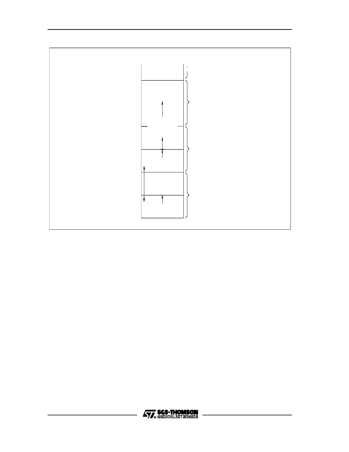
On-Chip RAM
The C167 incorporates a total of 2 KByte on-chip RAM, located in the address range
from 00F600h through 00FDFFh, shown in Figure 3. The stack size options are
extended accordingly, described in detail in section 3.3. The entire 2 KByte of internal
RAM can be used for variables, stack, and general purpose register banks.
C167 FAMILY PRELIMINARY USER MANUAL
25/180
Figure 3. On-Chip RAM Address Map
00 F600h
00 F700h
VR001891
00 FDFFh
Bit-
Addressable
Space
PEC Pointers
00 FD00h
00 FC00h
00 FB00h
00 FA00h
00 F900h
00 F800h
2 KByte
Dual Port RAM
used for
Registerbanks
Data
Stack Code
Stack Size Options:
ST10x66 Options
Additional

C167 FAMILY PRELIMINARY USER MANUAL
26/180
2.3
PEC Pointer Address Space
The source and destination pointers for the PEC channels, which in the ST10x166
occupy the bitaddressable address range 0FDE0h through 0FDFFh, are remapped in
the C167 to the address range 0FCE0h through FCFFh, as illustrated in Figure 3.
This change enables the user to utilize all 2048 bits in the RAM without having to
sacrifice this valuable space when using the PEC channels.
Note:
This change is an incompatibility with the ST10x166 !
2.4
Extended Special Function Register Space (ESFR)
In the C167, due to the amount of registers required to control the additional on-chip
peripherals, the address range for the special function registers (SFRs) is extended.
This new Extended SFR range, ESFR, is located in the address range 00F000h
through 00F1FFh. It has the same size as the normal SFR range, and it is also split
into a bitaddressable and a non-bitaddressable section.
Due to the special addressing modes available for SFRs, some exceptions have to
be taken into account when accessing registers in the ESFR space. SFRs can be
addressed via a 16-bit direct (MEM) or indirect address ([Rw]), via a bit address
(BITOFF), or via a short 8-bit address (REG). Accessing SFRs via a 16-bit address
(MEM or [Rw]) is no problem since they are easily distinguished by that address. The
short addressing modes (REG or BITOFF), however, implicitly use the fixed base
address of the normal SFR range, and the addressing capability with 8 bits is totally
occupied by this range.
Thus, a method is implemented to allow the short address access (REG or BITOFF)
also for the new ESFR range. Instead of a windowing option, where either one or the
other of the SFR ranges would be available, this method allows both ranges to be
accessible at the same time.
For this purpose, an Extend Register EXTR (EXTPR, EXTSR) instruction is
implemented. This instruction is required before an access to a register in the ESFR
range is made with a short addressing mode (see also Chapter 1, Instruction Set).
The tools will provide options to insert this instruction automatically depending on the
addressing mode used. The following examples show accesses to the normal and
the extended SFR ranges:

C167 FAMILY PRELIMINARY USER MANUAL
27/180
Example 1:
Direct MEM access to an ESFR: No EXTR instruction required
MOV
R0, #const16
; GPRs are directly accessible in both ranges
MOV
ODP2, R0
; mem, reg addressing mode for the ESFR ODP2
Example 2:
Direct REG access to an ESFR: EXTR instruction required
EXTR
#4
; Extend Register for the following four instructions
MOV
ODP2, #data16
; reg, #data16 addressing mode
BFLDL
DP6, #mask, #data8
; bitoff addressing mode
BSET
DP1H.7
; bitaddr (= bitoff+bitnr) addressing mode
MOV
XP0IC, R1
; mem, reg addressing mode (XP0IC via mem, R1 via reg)
; GPRs are always accessible in both ranges
; ==> EXTR scope not required for this instruction
Example 3:
Access to both SFR spaces: No EXTR instruction required
MOV
S0TBUF, SSCRB
; reg, mem: S0TBUF via reg, SSCRB via mem
MOV
SSCTB, S0RBUF
; mem, reg: SSCTB via mem, S0RBUF via reg
In order to optimize accesses to the ESFR space, the distribution of the special
function registers between the two SFR ranges was chosen such that the ESFR
space holds registers which are rarely used during normal program execution. These
registers are mainly only written to during the initialization of the peripherals, and are
in most cases accessed via direct MEM addressing. However, except for the
direction control registers of PORT0 and PORT1, only registers new in the C167 are
moved to the extended SFR space. This is done to provide compatibility with existing
designs.
With one new module, however, a retranslation or even rewriting of pieces of code is
necessary. The CAPCOM2 Unit is on one hand new in the C167, on the other hand it
is somehow an ’old’ peripheral, since it is equal to the CAPCOM1 Unit known from
the ST10x166. Due to the amount of registers required for this unit, it is not possible
to place all registers into the normal SFR space in order to use code written for the
CAPCOM1 Unit to be used for the CAPCOM2 Unit without any changes (except for
address modifications). To minimize the modification effort, mostly used CAPCOM2
registers, such as the capture/compare or the mode control registers, are located in
the normal SFR space, and rarely used registers are placed into the ESFR space.
Figure 4. Standard and Extended SFR Spaces
C167 FAMILY PRELIMINARY USER MANUAL
28/180
GPRs
Reserved
Reserved
FEh
F0h
90h
80h
10h
00h
8-Bit
Address
Address
16-Bit
F1DFh
100h
F120h
F000h
F020h
*
*
Except for Port 0 and 1 Direction Registers
Bit-
Addressable
Addressable
Non Bit-
Non Bit-
Addressable
Addressable
Bit-
FE20h
FE00h
FF20h
FF00h
FFDFh
16-Bit
Address
Address
8-Bit
00h
10h
80h
90h
F0h
FEh
CPU Reg.
GPRs
VR001892
Standard SFR space
Extended ESFR Space
CPU Reg.
Figure 4 shows an overview of both, the normal SFR space and the ESFR space.
One can see, that the two spaces are very similar. The General Purpose Register
area in the upper portion of the normal SFR space is also reflected in the ESFR
range. Thus, the GPRs are also available within an EXTR instruction sequence. Note
that the GPR area in both SFR spaces (the upper 16 word locations) must not be
accessed via a 16-bit address. Except for the PORT0 and PORT1 direction control
registers, the address range occupied by the CPU registers (FE00 - FE1E, and FF00
- FF1E) are reserved in the ESFR space.
Tables 2.4-1 and 2.4-2 at the end of the Manual list all the Special Function Registers
in the C167.
Note: With respect to some Special Function Registers, this is an incompatibility with
the ST10x166 !

C167 FAMILY PRELIMINARY USER MANUAL
29/180
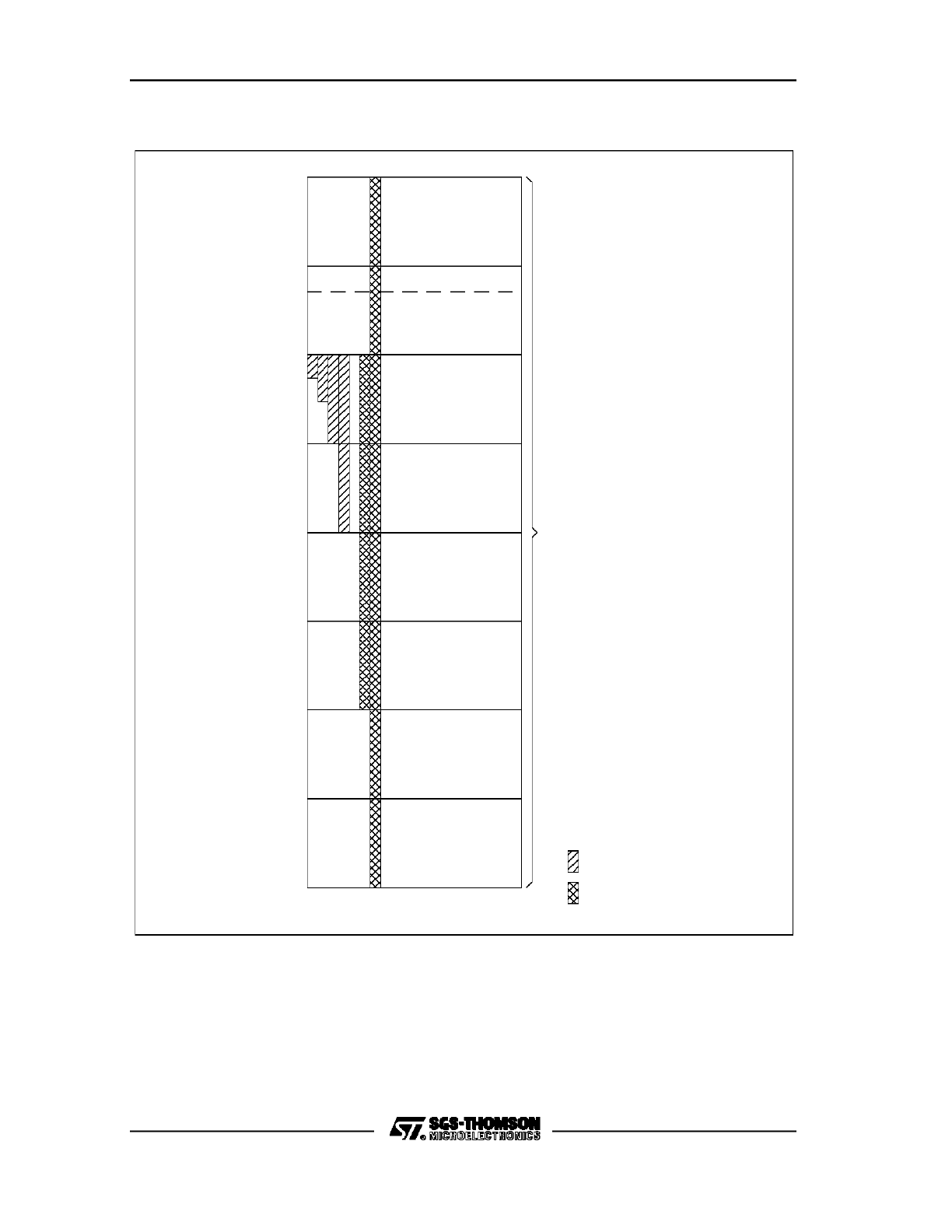
2.5
Internal Address Space
In the C167, the entire address range 00F000h through 00FFFFh in segment 0 is
mapped to internal addresses, that means, no external addresses will be generated
within this range. The right hand side of Figure 5 illustrates the different portions of
this area. Although the address space F200h through F5FFh is currently not used in
the C167, it is reserved for future expansion, and should not be used in an
application. An access to this area will result in a dummy access, and no external
addresses will be generated. The data of a write access will be lost, and a read
returns no valid data.
As already described in Chapter 2.1, the lower 32 KByte of either segment 0 or 1
(depending on ROM mapping) will also be mapped to internal addresses if the ROM
is enabled. The left hand side of Figure 5 shows the internal address spaces within
segment 0.
Note: This is an incompatibility with the ST10x166 !
C167 FAMILY PRELIMINARY USER MANUAL
30/180
Figure 5. Internal Address Space (Segment 0)
FE00h
FA00h
F200h
F000h
0000h
2000h
4000h
VR001893
F000h
FFFFh
Internal
8000h
ROM
(if enabled
and mapped
to Segment
0)
External
Memory
RAM, SFR
Extended
ESFR
Space
F600h
Reserved
Normal
SFR
Space
RAM
Dual Port
2 KByte
Internal Address Space
No External Addresses Generated

C167 FAMILY PRELIMINARY USER MANUAL
31/180
3.
BUS CONTROL UNIT
3.1
Extended Address Space
The C167 provides the full addressing capability of the ST10 family. The total
address space is extended to the maximum range of 16 MByte. This requires 24-bit
addressing, address lines A23..A0. The lower 16 bits of the address are provided via
Port 0 (in multiplexed bus mode) or via Port 1 (in non-multiplexed bus mode). The
upper 8 bits of the address are optionally provided via Port 4, which in the C167 is
extended to 8 bits (see Chapter 11).
The C167 has the capability of addressing up to 16 MByte, however, there are
several options for the user to configure the part for the number of physical external
address lines actually required in the system. First, one can switch between
segmented or non-segmented mode. In the non-segmented mode, the total address
range is 64 KByte, segment 0. Second, in the segmented mode, the user can specify
the number of segment address lines required in the system. Either 0, 2, 4, or all 8
segment address lines can be configured. By this, the user can select the external
address space addressable through physical external address lines to be either
64 KByte, 256 KByte, 1 MByte, or the full 16 MByte range. And third, up to five chip
select signals can be generated automatically to select several, different address
ranges. For example, the segment address lines may be limited to four lines, giving
direct addressing capability of up to 1 MByte, but the chip select signals can be used
to enable several blocks (or memory devices) of 1 MByte, giving a total address
range of, for instance, 5 MByte. Figure 6 shows such a configuration example.
C167 FAMILY PRELIMINARY USER MANUAL
32/180
Figure 6. Address Range Configuration Example
ST10167
I/O
1 MByte
Device 5
Device 4
1 MByte
1 MByte
Device 3
Device 2
1 MByte
Device 1
1 MByte
CS4
CS3
CS2
CS1
CS0
P4.7-P4.4
PORT 0
PORT 1
P4.3-P4.0
Example: Using 20 Address Lines and
5 Chip Selects to Access a
VR0D1646
Range of 5 MByte
D15-D0
Data Bus
A19-A16
A15-A0
Address Bus
The total address space is divided into code segments and data pages. Each code
segment has an address range of 64 KByte, thus there exist 256 code segments.
The currently active code segment is specified by the Code Segment Pointer, CSP,
which is modified only through any JMPS (Jump Segment) or CALLS (Call Segment)
instruction. The CSP is also extended to 8 bits, which represent address bits
A23..A16.

C167 FAMILY PRELIMINARY USER MANUAL
33/180
Since each data page has an address range of 16 KByte, there exist 1024 data
pages. To select the data pages, four Data Page Pointers, DPP0 through DPP3, are
available, giving access to four data pages at one time. The data page pointers are
selected through the two most significant bits of any 16-bit data address. Each of the
four data page pointers in the C167 is extended to 10 bits, which represent address
bits A23..A14. See also Chapter 1 for a scheme to bypass the segments and pages.
For more information on the data page pointers please refer to the ST10 User
Manual.
3.2
System and Bus Configuration Control
In the ST10x166, the SYSCON register is used to control the overall system
configuration and the external bus. In addition, the BUSCON1 register and the
associated ADDRSEL1 register allow the user to partition the address space for
external devices with different bus access parameters such as bus width, wait states,
etc. Now in the C167, five bus configuration registers, BUSCON0 through
BUSCON4,
and
four
address
range
select
registers,
ADDRSEL1
through
ADDRSEL4, are implemented, offering the option to have at least five address
ranges with different bus parameters, adapted to the needs of the memories or
peripherals located to these address ranges.
The SYSCON register known from the ST10x166 is separated into two registers in
the C167: Into one new BUSCON0 register, which is used for programming the bus
related parameters as with the other BUSCON registers, and into one SYSCON
register, which holds the bits to program the overall configuration of the system. With
this separation, it is now possible, for instance, to have the ALE lengthening feature
directly after reset, and to have a clear and transparent way of programming the
ROM mapping, bus enable, etc. In the following sections, the new registers are
described.
Note: This is an incompatibility with the ST10x166 !
3.2.1 SYSCON Register
The new SYSCON register is dedicated to global system functions, and is primarily
only written once during the initialization routine. The entire SYSCON register is
locked out from being written after the first occurrence of the EINIT instruction. This
improves system security such that if software were to unintentionally execute a write
access to this SFR, after the execution of the EINIT instruction, that it would be
ignored.
C167 FAMILY PRELIMINARY USER MANUAL
34/180
The new SYSCON register hereafter will occupy the bit addressable address
0FF12h. In the following, some important controls of the SYSCON register are
described.
SYSCON (FF12h/89h)
System Configuration Register
Reset Value: xxxxh
STKSZ
ROMS1
SGTDIS
ROMEN
BYTDIS
CLKEN
15
14
13
12
11
10
9
8
0
1
2
3
4
5
6
7
WRCFG
R
R
R
R
R
R
R
b15, b14, b13 = STKSZ: System Stack Size Selection.
b12 = ROMS1: ROM Segment Mapping control bit.
ROMS1 = 0: internal ROM mapped to segment 0.
ROMS1 = 1: internal ROM mapped to segment 1.
b11 = SGTIS: Segmentation Disable bit.
SGTDIS = 0: Segmentation enabled.
SGTDIS = 1: Segmentation disabled.
This bit does not control the number of Part 4 pins used.
b10 = ROMEN: ROM Enable bit.
ROMEN = 0: Internal ROM disabled, all instruction and data accesses to the ROM
space will be accessed externally.
ROMEN = 1: Internal ROM enabled, all instruction and data accesses to the ROM
space will access the ROM/FLASH.
b9 = BYTDIS: Byte High Enable (BHE#) pin control bit.
BYTDIS = 0: BHE# enabled.
BYTDIS = 1: BHE# disabled ; pin can be used for normal I/O.
b8 = CLKEN: System Clock Output (CLKOUT) Enable bit.
CLKEN = 0: CLKOUT disabled ; pin can be used for normal I/O.
CLKEN = 1: CLKOUT enabled ; pin used for system clock output.
b7 = WRCFG: Write Configuration Control Bit.
WRCFG = 0: Normal configuration of WR# and BHE#.
WRCFG = 1: WR# pin acts as WRL#, BHE# pin acts as WRH#.
b6 to b0 = R: Reserved.
Stack Size Parameters
The stack size selection is extended in the new SYSCON register from two to three
bits, due to the extended RAM space. The following table shows the possible options
for the stack:

C167 FAMILY PRELIMINARY USER MANUAL
35/180
SYSCON[15..13]
STKSZ
Maximum System
Stack Size
Address Range
0 0 0
256 Words
FA00h - FBFFh
0 0 1
128 Words
FB00h - FBFFh
0 1 0
64 Words
FB80h - FBFFh
0 1 1
32 Words
FBC0h - FBFFh
1 0 0
512 Words
F800h - FBFFh
1 0 1
reserved
reserved
1 1 0
reserved
reserved
1 1 1
No Wrapping
F600h - FDFFh
Entire internal RAM (see Note)
As one can see from this table, the internal system stack may be mapped to the
single port RAM area. Stack size options 0..4 mean that the stack will always reside
in the specified address range, there is a wrap-around mechanism implemented for
the stack (although the contents of the stack pointer itself will not perform this
wrapping; see ST10 User Manual). When the No Wrapping option is selected, the
stack may occupy the entire internal RAM space, from 00F600h to 00FDFFh. In this
case, the Stack Underflow and Overflow SFRs should be used to ensure that
unintentional accesses do not occur. In all cases, the internal system stack can
never be mapped to external memory.
Note: Special care must be taken when the no wrapping option is selected. In this
case, the Stack Pointer, SP, can be loaded with any word address between F000h
and FFFEh. No hardware protection exists against address values which are
occupied by either the reserved address space, or the standard or extended SFR
ranges, thus, the SP must never be loaded with addresses in the range F000h
through F1FEh (ESFR space), F200h through F5FFh (reserved space), and FE00h
through FFFEh (SFR space), otherwise unexpected results will occur!
Segmentation Control
As in the ST10x166, the bit SGTDIS controls whether segmentation is enabled or
not. After reset, this bit is ’0’, thus segmentation is enabled. However, different to the
ST10x166, this bit does not automatically configure port P4 to output the segment
address lines (this is performed through the system startup configuration, described
in section 3.5). The SGTDIS bit in the C167 is only used to enable segment
addresses to port P4, and to determine the correct stack operations for traps and
interrupts (optionally push/pop the Code Segment Pointer, CSP).

C167 FAMILY PRELIMINARY USER MANUAL
36/180
ROM Enabling and Mapping
The ROM Enable bit, ROMEN, determines whether the on-chip ROM is enabled or
not. This bit is set automatically during reset according to the state of the External
Access input pin, EA#. If this pin is high during reset, ROMEN will be set to ’1’, and
the C167 will start execution out of the internal ROM. A low level at this pin during
reset will force the C167 to start execution out of external memory, with external bus
parameters determined through the System Startup Configuration Selection (see
section 3.5). Bit ROMEN will be cleared in this case.
For the mapping of the internal ROM to either segment 0 or segment 1, other than in
the ST10x166, an individual bit, ROMS1, is implemented. The default after reset is
ROMS1 = 0, mapping the ROM to segment 0. If the ROM is enabled, one has to take
care of that no external addresses will be generated in the lower 32 KByte address
space of either segment 0 (ROMS1 = 0) or segment 1 (ROMS1 = 1).
Note that, until the execution of the EINIT instruction, the default values in the
SYSCON register can be changed through software. One has to take care, however,
that bits ROMEN and ROMS1 should never be changed when executing out of the
on-chip ROM, otherwise unexpected results may occur.
Note: The Write Configuration (WRCFG) control is explained in detail in section 3.4.
3.2.2 BUSCON0 Register
As mentioned above, the bus related control bits of the ST10x166 SYSCON register
are moved to a new BUSCON0 register in the C167. This register is shown hereafter.
This change allows to organize the BUSCON0 register in the same way as any other
BUSCON register, giving the same functionality and a consistent way of
programming.
BUSCON0 (FF0Ch/86h)
Bus Configuration Register 0
Reset Values: 0000h/ 0600h/ 0640h/ 0680h/ 06C0h
RDYEN0
R
BUSACT0
ALECTL0
R
15
14
13
12
11
10
9
8
0
1
2
3
4
5
6
7
MTTC0
RWDC0
0
0
R
BTYP
MCTC

C167 FAMILY PRELIMINARY USER MANUAL
37/180
b15, b14 = 0.
b13 = R: Reserved.
b12 = RDYEN0: READY# Input Enable control bit.
RDYEN0 = 0: READY# function disabled for BUSCON0 accesses.
RDYEN0 = 1: READY# function enabled for BUSCON0 accesses.
b11 = R: Reserved.
b10 = BUSACT0: Bus Active control bit.
b9 = ALECTL0: ALE Lengthening control bit.
b8 = R: Reserved.
b6, b7 = BTYP: External Bus Configuration Control.
b5 = MTTC0: Memory Tri-state Time Control.
b4 = RWDC0: Read/Write Delay Control.
b3 to b0 = MCTC: Memory CYcle Time Control.
If during reset, the EA# pin is at a high level, the BUSCON0 register is cleared to
’0000’, and execution begins out of the on-chip ROM. An external bus can then be
selected via programming the BUSCON0, BUSCON1..4, and ADDRSEL1..4 registers
appropriately.
If the EA# pin is low, forcing execution to start with external memory, register
BUSCON0 is set according to the selected bus type, with default values for the bus
parameters:
MCTC
= 0000
15 Memory Cycle Time Waitstates
RWDC0
= 0
Read/Write Delay Enabled
MTTC0
= 0
One Memory Tri-State Waitstate
BTYP
= XX
set according to the level at pins P0xx and P0xx during reset
ALECTL0 = 1
ALE Lengthening Enabled
BUSACT0
= 1
External Bus Enabled
RDYEN0 = 0
READY# Input Disabled
The coding of the BTYP bits in the BUSCON0 (and also in registers BUSCON1..4) is
changed compared to the ST10x166. The new BTYP coding is shown in the
following:
BTYP
Selected Bus Operation
0 0
0 1
1 0
1 1
8-Bit Non-Multiplexed Bus
8-Bit Multiplexed Bus
16-Bit Non-Multiplexed Bus
16-Bit Multiplexed Bus

C167 FAMILY PRELIMINARY USER MANUAL
38/180
With this coding, a clear reference of a BTYP bit to the selected operation is given.
BTYP.1 controls the width of the bus (8-bit or 16-bit), while BTYP.0 controls whether
the bus is multiplexed or non-multiplexed. In addition, this coding directly reflects the
default bus configuration selection during reset at the P0 pins (see System Startup
Configuration).
One can see that, other than in the ST10x166, external execution will start with the
ALE lengthening enabled, offering the slowest possible bus. The user can reprogram
the bus parameters during the initialization (or during normal run time) to values
required by the external hardware.
Other than for the bus configuration registers BUSCON1..4, the BUSCON0 register
has no associated address select register ADDRSEL. Instead, the BUSCON0
register controls the bus for any external accesses to addresses which are not
covered by one of the address select register, i.e. it fills the gaps between these
address ranges.
To indicate an external access controlled through the BUSCON0 register, and to
allow a simple selection of the memory or peripheral, an individual chip select line,
CS0#, is assigned to the BUSCON0 register. If CS0# is enabled (through System
Startup Configuration, see section 3.5), it goes to a low level for each external
access controlled through BUSCON0, i.e. for each external access outside the range
of the ADDRSEL registers. It will go to a high level for each other access. See
section 3.3 for details on the chip select lines.
3.2.3 BUSCON1..4 and ADDRSEL1..4 Registers
Hereafter is shown the configuration of a BUSCON1..4 register. Although these
registers look similar to the BUSCON0 register, some differences exist. Each of the
BUSCON1..4 registers has an associated ADDRSEL1..4 register, which specifies the
active address range for this BUSCON register. That means, for an external access
to an address range specified through an ADDRSELx register, the parameters of the
bus are controlled by the respective BUSCONx register.
The second difference is the initialization after reset. The BUSCON1..4 registers are
always initialized to all ’0000’, while the BUSCON0 register is loaded according to the
selected startup configuration during reset.
A further difference between the BUSCON1..4 and the BUSCON0 registers is in the
options for the chip selects, detailled in Chapter 3.3.

C167 FAMILY PRELIMINARY USER MANUAL
39/180
Note: Special care must be taken when programming the BUSCON registers. An
external bus will be enabled as long as at least in one of the BUSCON register the
BUSACTx bit is set. Port 1 will be used for address output if at least through one of
the BUSCON registers a non-multiplexed bus is selected. Port 1 will also continue to
output the addresses for an access via a multiplexed bus, controlled through another
BUSCON register.
BUSCON1 (FF14h/8Ah)
Bus Configuration Register 1
Reset Value: 0000h
RDYEN1
R
BUSACT1
ALECTL1
R
15
14
13
12
11
10
9
8
0
1
2
3
4
5
6
7
MTTC1
RWDC1
CSREN1
R
BTYP
MCTC
CSWEN1
b15 = CSWEN1: Write Chip Select Enable control bit.
b14 = CSREN1: Read Chip Select Enable control bit.
B13 = R: Reserved.
b12 = RDYEN1: READY# Input Enable control bit.
RDYEN1 = 0: READY# function disabled for BUSCON1 accesses.
RDYEN1 = 1: READY# function enabled for BUSCON1 accesses.
b11 = R: Reserved.
b10 = BUSACT1: Bus Active control bit.
b9 = ALECTL1: ALE Lengthening control bit.
b8 = R: Reserved.
b7, b6 = BTYP: External Bus Configuration Control.
b5 = MTTC1: Memory Tri-state Time Control.
b4 = RWDC1: Read/Write Delay Control.
b3 to b0 = MCTC: Memory Cycle Time Control.
For each BUSCON1..4 register, an individual chip select line CS1#..CS4# is
associated to save external glue logic for chip select generation. If a CSx# is enabled
(through System Startup Configuration, see section 3.5), the signal will go low for any
external access in the range defined through the respective address select register
ADDRSELx. It will go to a high level for any internal access or accesses outside the
specified address range.
In order to support the extended address range of 16 MByte, the possible address
range selections in the Address Select Registers ADDRSEL1..4 are also extended.
The Range Size field now allows the selections shown in the following table. This
table also shows the reference between the range size and the range start address.

C167 FAMILY PRELIMINARY USER MANUAL
40/180
All sixteen bits of the ADDRSEL registers are now used for the specification of the
address range for a BUSCON register. Note that the relevant bits (R) define the
associated upper address bits of the selected address range, they are associated
with address lines A23..A12. One can see that the upper 8 bits of the ADDRSEL1..4
registers directly relate to the respective code segment (A23..A16). The bits marked
with ’x’ are don’t care bits.
Range Size
RGSZ
Selected Address
Range
Relevant (R) bits of
Range Start Address RGSAD
0 0 0 0
4 KByte
RRRRRRRRRRRR
0 0 0 1
8 KByte
RRRRRRRRRRR x
0 0 1 0
16 KByte
RRRRRRRRRR xx
0 0 1 1
32 KByte
RRRRRRRRR xxx
0 1 0 0
64 KByte
RRRRRRRR xxxx
0 1 0 1
128 KByte
RRRRRRR xxxxx
0 1 1 0
256 KByte
RRRRRR xxxxxx
0 1 1 1
512 KByte
RRRRR xxxxxxx
1 0 0 0
1 MByte
RRRR xxxxxxxx
1 0 0 1
2 MByte
RRR xxxxxxxx x
1 0 1 0
4 MByte
RR xxxxxxxxx x
1 0 1 1
8 MByte
R xxxxxxxxxxx
1 1 x x
reserved
Note: In order to allow sections of 4 and 8 KByte, and to implement a more general
scheme, the ADDRSEL register organization has been rearranged, compared to the
ST10x166. The smallest section will be 4 KByte (instead of 2 KByte in the
ST10x166), the Range Size field is now 4 bits, and the Start Address field is now 12
bits. Although this leads to incompatibility with existing programs, the advantages
justify this change.
Note: This is an incompatibility with the ST10x166 !
Hereabove is the bus configuration register BUSCON1, while the associated address
range select register ADDRSEL1 is shown herafter:
C167 FAMILY PRELIMINARY USER MANUAL
41/180
ADDRSEL1 (FE18h/0Ch)
Address Select Register 1
Reset Value: 0000h
15
14
13
12
11
10
9
8
0
1
2
3
4
5
6
7
RGSZ
RGSAD [11..4]
RGSAD
b15 to b4 = RGSAD: BUSCON1 Address Range Start Address Selection.
b3 to b0 = RGSZ: BUSCON1 Address Range Selection.
Registers BUSCON2..4 and ADDRSEL2..4 are organized in the same manner. For
more details on the BUSCON and ADDRSEL registers please refer to the ST10 User
Manual. The address locations of these registers in the SFR space are as follows:
Register
Physical
Address
8-Bit
Address
Note
BUSCON0
0FF0Ch
86h
bitaddressable
BUSCON1
0FF14h
8Ah
bitaddressable
BUSCON2
0FF16h
8Bh
bitaddressable
BUSCON3
0FF18h
8Ch
bitaddressable
BUSCON4
0FF1Ah
8Dh
bitaddressable
ADDRSEL1
0FE18h
0Ch
not bitaddressable
ADDRSEL2
0FE1Ah
0Dh
not bitaddressable
ADDRSEL3
0FE1Ch
0Eh
not bitaddressable
ADDRSEL4
0FE1Eh
0Fh
not bitaddressable
Note that, due to the fact that the bus parameter bits are more often affected by
software than the other system control bits, the BUSCON0 register in the C167 is
placed on the same SFR address as the SYSCON register in the ST10x166. This
requires the least amount of changes in existing software when transferred to the
C167. The new SYSCON register in the C167 is located to a new SFR address,
FF12h / 89h.
Note: One must never program two or more ADDRSEL registers such, that the
selected address ranges overlap either entirely or partially, otherwise unexpected
results may occur. An exception to this restriction, of course, is the address range for
the BUSCON0 register. This register controls the bus for any accesses outside the
ranges defined through the ADDRSEL register. If no other BUSCONx register selects
a bus in a specific address range, the external bus in the entire address range of up
C167 FAMILY PRELIMINARY USER MANUAL
42/180
to 16 MByte is controlled by the BUSCON0 register. Thus, programming another
BUSCON to a certain address range always overlaps the BUSCON0 address range,
however, this is an intended, implemented operation, and no problems will occur in
this case. It can be regarded in this way, that the BUSCON1..4 and ADDRSEL1..4
registers have the same level of priority among them (thus it is not possible to
determine the preference in an address overlap case), while BUSCON0 has a lower
priority. It is possible, however, to overlap an ADDRSEL address range with an
internal (ROM, RAM, SFR, ESFR, etc.) address range. In this case, accesses to
addresses in the overlapping regions are always made to the internal space.
Figure 7. BUSCON Configuration Examples
BUSCON0, CS0
16M
12M
8M
4M
1M
0K
BUSCON2
BUSCON0,CS0
(Range 4K, Start 0K) CS0
0K
4K
8K
16K
32K
VR001898
Non-Segmented Mode
Segment Mode
4K, CS2
BUSCON4
4MByte
CS4
CS1
4MByte
BUSCON1
BUSCON3
4MByte
CS3
BUSCON0
48K
64K
BUSCON1
BUSCON2
BUSCON0
BUSCON3
BUSCON4
(Range 8K, Start 16K) CS0
Range 8K
Start 24K, CS3
Start 8K, CS2
Range 8K
Range 4K
Start 4K, CS1
Start 32K, CS4
Range 32K
Example
Example

C167 FAMILY PRELIMINARY USER MANUAL
43/180
3.3
Chip Selects
In order to save external glue logic mostly required for the generation of separate
chip select signals for external devices such as memories or peripherals, on-chip
automatic chip select signal generation is implemented in the C167. For this purpose,
each BUSCON register (also the new BUSCON0 register) is designated a port line
(see Chapter 11), which provides a chip select signal as an alternate function. When
a chip select output is enabled for a BUSCONx register (see Chapter 3.5 for
enabling/disabling chip selects), the associated output pin will go to a low level each
time an external access to an address in the specified range for this BUSCONx
register is performed. The pin returns to a high level for any access outside of the
specified range and for internal accesses.
Each BUSCONx register is assigned a chip select line CSx#. Chip selects
CS1#..CS4# will go active (if enabled) when an external access within the address
range specified through the associated ADDRSELx register is performed. Chip select
line CS0#, which is associated to the BUSCON0 register, will go active (if enabled)
for
any
external
access
outside
the
ranges
specified
through
registers
ADDRSEL1..4.
For chip selects CS1#..CS4#, two different options exist, selectable through bits 15,
CSWENx, and 14, CSRENx, of the respective BUSCON1..4 registers. This is
illustrated in the following table (see also Figures 8 and 9). These options are
described in detail in the next sections. Note that for the BUSCON0 chip select line
CS0#, these options are not available. The reason is that if CS0# is enabled during
reset (see Chapter 3.5), it must go active directly after reset to enable fetching of the
first instructions. There is no way to additionally select whether CS0# should operate
as address or read/write chip select directly after reset. Furthermore, since
BUSCON0 and CS0# are nearly in all cases used to access code memory, such a
chip select option is not useful.
CSWENx
CSRENx
Chip Select Operation (Chip Selects CS1#..CS4#)
0
0
Address Chip Select
0
1
Read Chip Select
1
0
Write Chip Select
1
1
Read/Write Chip Select
Note that the chip selects, whether Address or Read/Write Chip Selects, will not be
generated for internal accesses, even if the access is to an address within the range
specified through an ADDRSEL register.

C167 FAMILY PRELIMINARY USER MANUAL
44/180
In order to avoid undefined levels of pins used as chip select lines, internal pullup
devices of about 50 KOhm are implemented at these pins. This pullups are switched
on during reset (either hardware, software, or watchdog timer reset), such that these
lines are held at a high level. After the reset sequence has been finished, the pullup
devices are switched off. The lines selected for chip select operation are then be
automatically switched to the output mode and drive the appropriate level. The pins
not configured for chip select operation will return to the high-impedance state.
When an HOLD# is requested by an external device, then besides switching the
address and data bus to the high impedance mode, the C167 also turns the chip
select signals off when generating the acknowledge signal HLDA#. This enables the
external master to not only control the address and data bus, but to also use the
same chip select lines to access the individual external devices connected to the
bus. The chip selects can be turned off in such a case in two ways, controlled
through the respective Open Drain Control register (see section 11.6) for the port: If
the respective control bit ODPx.y is ’0’, the chip select line will be held high through
switching on the internal pullup device at this pin. If ODPx.y = 1, this pullup device will
not be activated, the pin will float to the high-impedance state. Either an external
pullup device has to be connected in this case or the external master is capable of
pulling the lines to an appropriate level.
3.3.1 Address Chip Selects
A chip select, which is generated by decoding the address lines, and which is
activated for the whole duration of an external bus cycle, is named an Address Chip
Select in the context of this paper. This is done to distinguish it from the Read/Write
Chip Selects described in the next section.
The activation of an Address Chip Select is selected with CSWENx = CSRENx = 0
(default after reset) in the BUSCON registers (Note that for CS0#, this is the only
option; the respective bits in BUSCON0 are reserved). When an access within the
address range specified by the associated ADDRSEL register is performed, the
respective chip select line CSx# (x= 0..4) will go to a low level with the falling edge of
ALE, and remain at this level until an access outside of this range is made. It will then
be deactivated again with the falling edge of ALE of the bus cycle accessing the new
range. No spurious spikes will be generated on the chip select lines. Figure 8 shows
the timing of the address chip select signals.
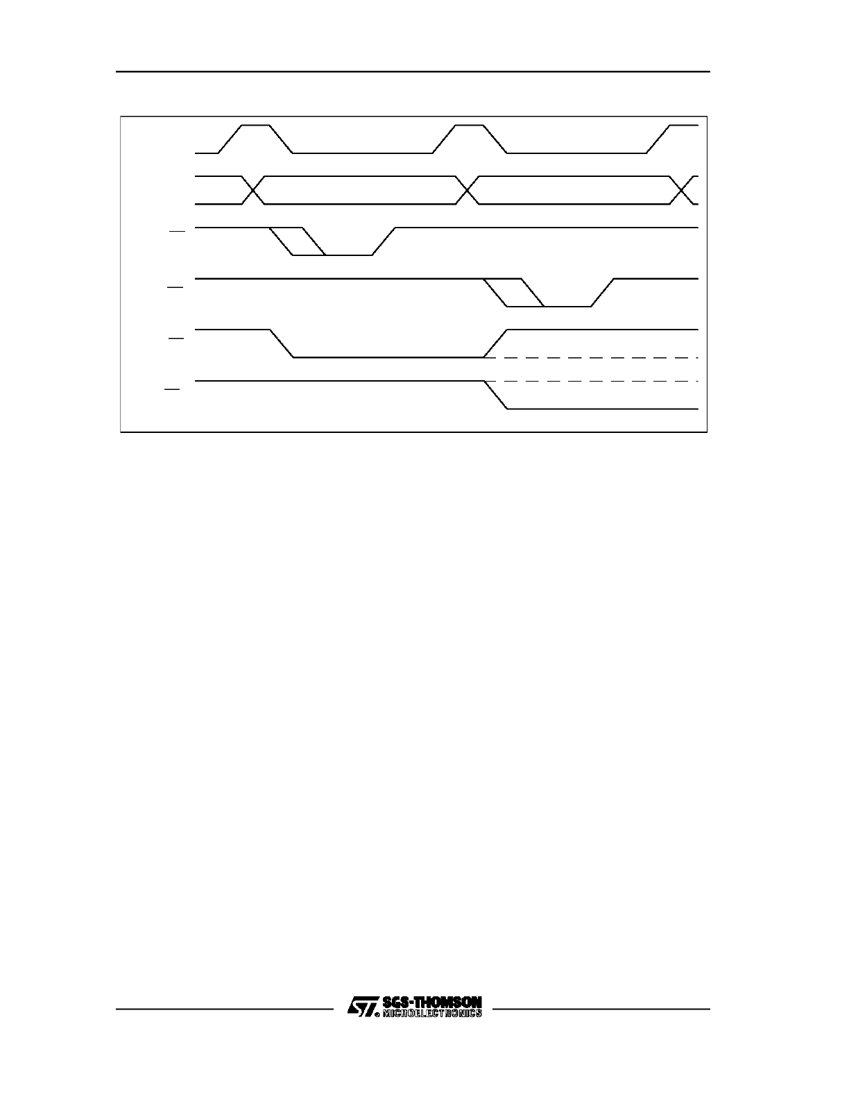
C167 FAMILY PRELIMINARY USER MANUAL
45/180
Figure 8. Address Chip Select Operation (MUX-Bus Example)
VR001894
ALE
CSy
ADDRESS
BUS
RD
WR
CSx
3.3.2 Read/Write Chip Selects
For accessing external devices such as latches or direction drivers, which often only
have one enable input, another chip select option is implemented. This option allows
to internally gate the chip select signal derived from the addresses with the read or
write signal. This means, for example, that a write chip select signal will only be
generated when writing to a specific address range, not for a read access to this
range, and that it has the same timing characteristics as the write signal. Figure 9
shows the timing for these read/write chip select signals. There are three selectable
options. The chip select can be generated either only for read accesses (CSRENx =
1, Read Chip Select), or only for write accesses (CSWENx = 1, Write Chip Select), or
for both, read and write accesses (CSRENx & CSWENx = 1, Read/Write Chip
Select). This feature saves external glue logic when accessing devices with only one
enable input. Figure 10 shows two examples for this.
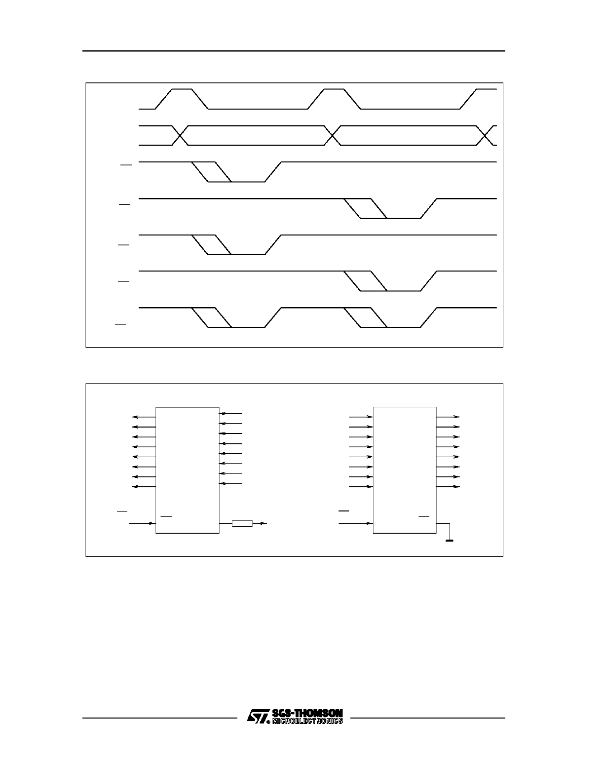
C167 FAMILY PRELIMINARY USER MANUAL
46/180
Figure 9. Read / Write Chip Select Operation (MUX-Bus Example)
VR0A1894
ALE
ADDRESS
BUS
RD
WR
CSx
READ
WRITE
CSx
CSx
WRITE
READ/
Figure 10. Read / Write Chip Select Examples
8-Bit
Latch
e.g.
HC573
OC
C
Data
Output
D7...D0
Read CS
e.g.
Input
Data
DIP-
C
OC
HC574
e.g.
Latch
8-Bit
Switches
D7...D0
Data
Input
e.g.
D7...D0
Output
Data
Write CS
+5V
VR001895
a: Read Chip Select Example
b: Write Chip Select Example
Note: When the WRH#/WRL# option (see next chapter) is selected, the Write or
Read/Write Chip Select will go active if any of the WRH# or WRL# signals goes
active. There will be no distinction between writing to the low byte, to the high byte, or
to both. The read/write chip selects will also be affected by the read/write delay
control RWDCx of a BUSCONx register.
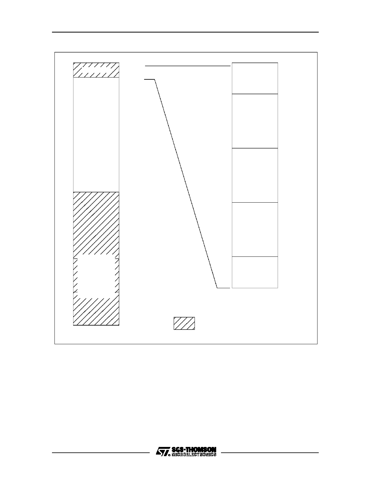
3.4
Byte High Enable or Write High , Write Low Operation

C167 FAMILY PRELIMINARY USER MANUAL
47/180
When writing bytes to external word-wide memories or peripherals (regardless
whether they are true word-wide devices or two 8-bit devices in parallel), a distinction
has to be made between writing to the low or to the high byte, or to both. For this
purpose, the address line A0 and the Byte High Enable signal BHE# are used to
properly select either half or both halfs of the device. Figure 11 shows an example for
this connection, where the chip select signal is gated with A0 and BHE# (see also the
ST10 User Manual).
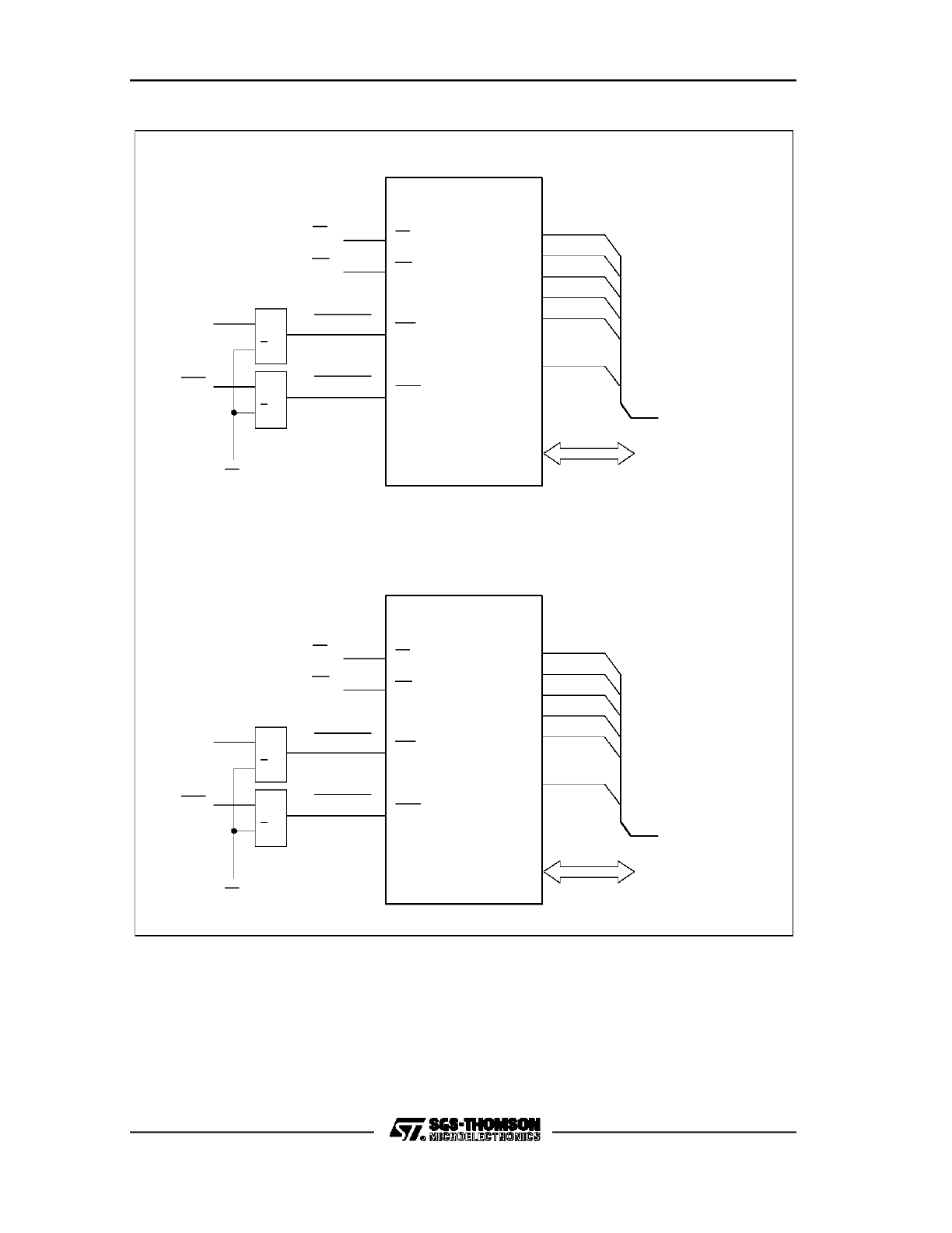
C167 FAMILY PRELIMINARY USER MANUAL
48/180
Figure 11. Connection Possibilities of an External Read / Write Device
RD
WR
> 1
CS-LOW
CS-HIGH
1
>
A0
BHE
CS
(from Decoder)
WR
RD
CSL
CSH
A1
A2
A0
A1
A3
A2
A4
A3
A5
A4
An-1
An
16-Bit Device
D0...D15
D0...D15
Data Bus
a: Separate Chip Select Inputs
b: Separate Write Strobe Inputs
Data Bus
D0...D15
D0...D15
16-Bit Device
An
An-1
A4
A5
A3
A4
A2
A3
A1
A0
A2
A1
WRH
WRL
RD
CS
(from Decoder)
WR
BHE
A0
> 1
WR-HIGH
WR-LOW
1
>
CS
RD
Address Bus
Address Bus
VR001896

C167 FAMILY PRELIMINARY USER MANUAL
49/180
Besides devices with two chip select inputs, which can be connected via the method
described above, there exist a number of external 16-bit devices which have only
one chip select input, but two separate write inputs: a Write Low Byte (WRL#) and a
Write High Byte (WRH#) input. Connecting these devices can be done as illustrated
in Figure 11b.
As it can be seen, both methods require external glue logic, and it is very desirable to
save these gates and have integrated solutions instead. To integrate separate chip
selects for low or high byte instead of BHE# and A0 (Figure 11a) would require
double the number of chip selects and pins, which are not available in the C167.
Integrating the second method, however, does not require additional pins, since the
write signals run parallel to all read/write devices. Thus, this method was chosen for
implementation. The C167 will incorporate an option to automatically generate a
WRL# and WRH# signal instead of WR# and BHE#. This option can be selected via
the control bit WRCFG, Write Configuration (SYSCON.7). When this bit is set, the
WR# pin will be configured as a Write Low Byte (WRL#) strobe, and the BHE# pin as
a Write High Byte (WRH#) strobe. The following table shows the resulting
relationship:
WR#/
WRL#
BHE#/
WRH#
Operation
0
0
Write to a word (Low and High byte)
0
1
Write to the low byte
1
0
Write to the high byte
1
1
No write access (either read or no access)
Figure 12 shows the timing of these signals compared to the default mode (WR# and
BHE#). Note that after reset, the default mode is the WR#/BHE# operation. If the
BYTDIS bit (BHE# Pin Disable bit, SYSCON.9) is set, also the WRH# operation, if
selected, is disabled. The pin can then be used for general purpose I/O.
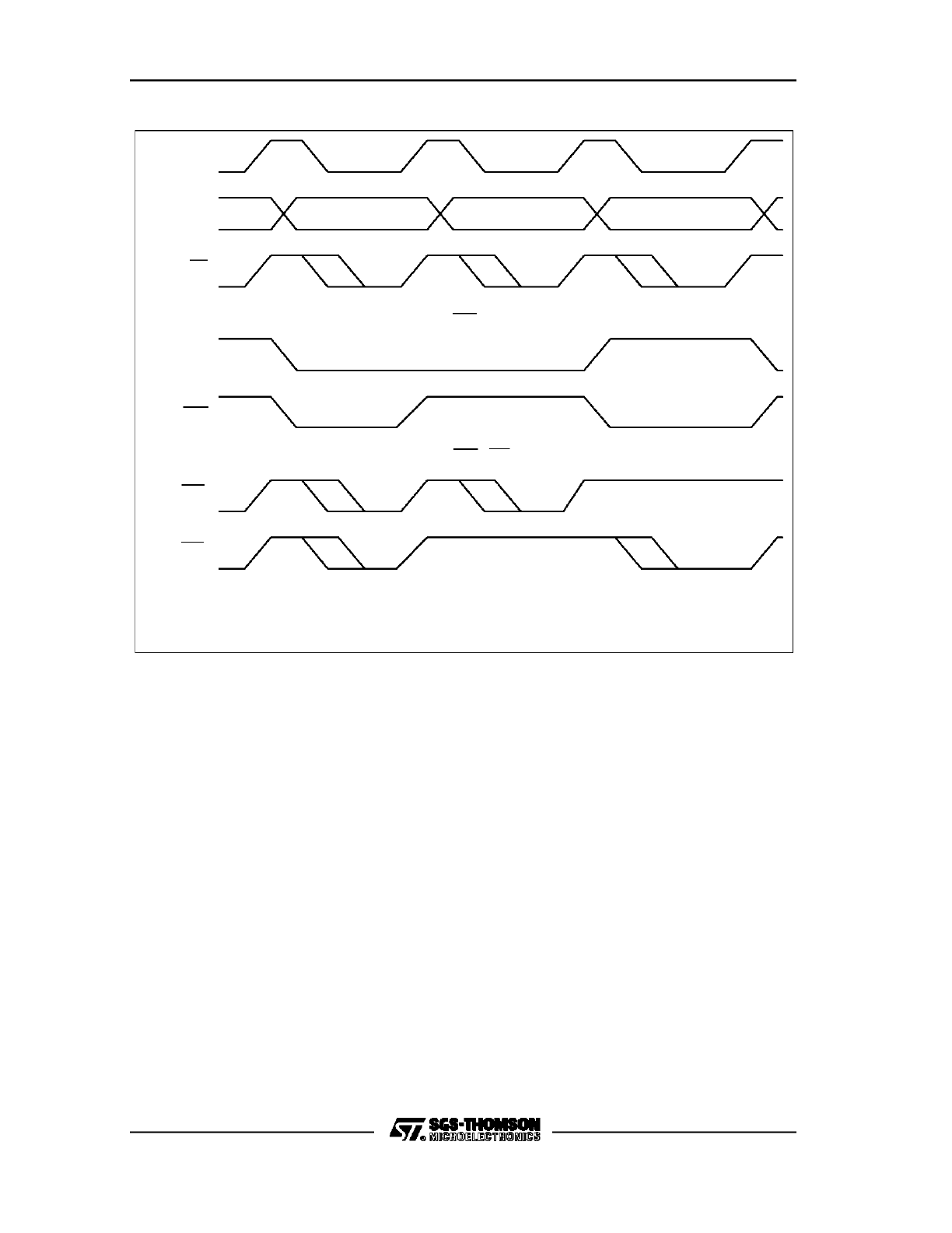
C167 FAMILY PRELIMINARY USER MANUAL
50/180
Figure 12. BHE#/A0 versus WRH#/WRL# Operation (DEMUX-Bus Example)
VR001897
ALE
ADDRESS
BUS
A0
WR
BHE/A0 OPERATION
BHE
WRH / WRL OPERATION
WRL
WRH
WRITE ACCESS TO A
WRITE ACCESS TO A
WRITE ACCESS TO A
WORD
LOW BYTE
HIGH BYTE
If the WRH#/WRL# option is selected, and an access via an 8-bit data bus is
performed, the WRL# signal is activated for every write access, while the WRH#
signal is activated only for high byte accesses (A0 = 1).
Note: When the WRH#/WRL# option is selected, the two signals are also affected by
the read/write delay control RWDCx in a BUSCONx register.
Note: This distinction between the low byte or high byte is only necessary for write
accesses to external memory or peripherals. For read accessses, always the entire
word can be read; the C167 itself determines whether to read the lower or upper byte
from the 16-bit data bus. There might be rare cases, however, where the reading of a
byte might affect status information in a peripheral (for example, reading an interrupt
pending register clears the request flags automatically). In this case it might be
necessary to use A0 and BHE# also for read accesses, such that only the addressed
byte is read. The WRH#/WRL# option cannot be used then.

C167 FAMILY PRELIMINARY USER MANUAL
51/180
3.5
System Startup Configuration
In the ST10x166, three dedicated pins, EBC0, EBC1, and BUSACT#, are used
during reset to configure the bus operation of the chip. The further configuration,
such as segmentation, is done such that a default configuration is automatically
assumed. For example, the default configuration is segmentation enabled, causing
the two pins of Port 4 to output address bits A16 and A17, which are at ’0’ after reset.
Users not requiring segmentation have to take care of this effect when using Port 4
for general purpose I/O. This is a minor disadvantage for these users.
In the C167, when keeping with this scheme, all 8 pins of Port 4 will output ’0s’, the
full address of segment 0, directly after reset. The problem for users requiring no
segmentation would increase. In addition, in the C167, some more startup
initializations, such as chip selects enabled/disabled, have to be performed. These
considerations resulted to the following new scheme for setting up the system
configuration during/after reset:
Instead of three pins, only one dedicated pin, EA# (External Access), will be used to
determine whether the chip will start with internal ROM or external memory. The lines
of PORT0 are then used during reset to configure the system, such that the state of
the PORT0 pins read during reset determines the system startup configuration.
The pins of PORT0 (i.e. P0L and P0H) contain weak pullup devices (ca. > 100
KOhm) which are switched on during the entire time that a reset sequence is active
(this is true for any hardware, software, or watchdog timer reset), and pull the pins to
a high level. The state of these pins are read during reset. If all pins are read as ’1’, a
default configuration is selected. If a different configuration is required, this can be
selected by pulling individual PORT0 lines low during reset with external pulldown
devices of ca. 15 KOhm. After the reset sequence has terminated, the internal pullup
devices at PORT0 are switched off. If external pulldown devices are connected to
individual PORT0 pins, they can be left connected also after reset if no corruption of
the function of the PORT0 pins can occur. Special care should be taken with respect
to output load and voltage levels when using values of less than 15 KOhm.
Note: The current DC specification for the output voltages VOH in the Data Sheet
specify an output voltage of VOHmin of 0.9 VCC at an output current IOH of -100 uA.
Using an external pulldown device of 15 KOhm would violate this specification, since
the current drawn through this pulldown is much higher. However, characterizations
have shown that the output drivers are strong enough to hold the specified output
voltage also at higher currents. To avoid a violation of Data Sheet parameters, it is
planned to increase the specification of IOH in the Data Sheet to an appropriate
value.

C167 FAMILY PRELIMINARY USER MANUAL
52/180
The following Table 3.5 illustrates the relationship between a PORT0 pin and the
associated system configuration:
Table 3.5: PORT0 Pin Assignment for System Startup Configuration
Pin
Selection for
Sampled with
P0L.0
Emulation Mode
Hardware Reset
P0L.1
Adapt-Mode
Hardware Reset
P0L.2
P0L.3
reserved
P0L.4
Bootstrap Loader Mode
Hardware Reset
P0L.5
reserved
P0L.6
Bus Mode
Hardware, Software, and Watchdog Timer Reset
P0L.7
Bus Data Width
Hardware, Software, and Watchdog Timer Reset
P0H.0
reserved
P0H.1
P0H.2
Number of Chip Selects
Hardware, Software, and Watchdog Timer Reset
P0H.3
P0H.4
Number of Segment
Address Lines
Hardware, Software, and Watchdog Timer Reset
P0H.5
P0H.6
P0H.7
reserved
The default configuration for the bus operation is as follows:
-
Multiplexed Bus
-
16-Bit Data Bus
-
2-Bit Segment Address at Port 4 (18-Bit total Address)
-
Five Chip Select Outputs (CS0#, CS1#, CS2#, CS3#, CS4#)
C167 FAMILY PRELIMINARY USER MANUAL
53/180
One can see that the configuration selection is chosen such, that in most cases a
minimum number of external pulldown devices is required. For example, only one
pulldown resistor is required to select either a non-multiplexed 16-bit bus, or a
multiplexed 8-bit bus. The maximum number of pulldowns would be required for the
very unlikely case of an initial 8-bit non-multiplexed bus with three chip select lines
and a 4-bit segment address.
The startup configuration is continuously sampled during reset, however, the last
value sampled before the reset sequence is terminated is taken as valid. This
configuration is then latched internally, in different ways and at different locations.
The state of the PORT0 lines P0H[0..7] is latched into a special register, RP0H
(ESFR space, address 0F108h/84h).
RP0H (F108h/84h)
System Startup Configuration Register (Read-Only)
Reset Value: xxxxh
0
1
2
3
4
5
6
7
CSSEL
R
R
R
SALSEL
R
b7 to b5 = R: Reserved.
b4,
b3 = SALSEL: Number of Segment Address Lines configured during reset
(read-only).
b2, b1 = CSSEL: Number of Chip Select Lines configured during reset (read-only).
b0 = R: Reserved.
Bus Mode and Data Width Selection
If external start of execution is selected (EA# = 0), PORT0 lines P0L[6..7] are used to
define the initial bus mode of the C167. The state of these two pins sampled at the
end of the reset sequence is copied into the bus type field of the BUSCON0 register.
P0L.7 determines the data width of the bus, while P0L.6 controls whether a
multiplexed bus or a non-multiplexed bus is used. These values can be changed
after reset at any time via a write instruction to BUSCON0.
P0L.7
P0L.6
Selected Bus Type
1
1
0
0
1
0
1
0
Multiplexed 16-Bit Bus (Default)
Non-Multiplexed 16-Bit Bus
Multiplexed 8-Bit Bus
Non-Multiplexed 8-Bit Bus
Depending on the selected initial bus mode, PORT0 and PORT1 will be automatically
switched into the appropriate mode directly after reset.

C167 FAMILY PRELIMINARY USER MANUAL
54/180
Note: If an initial 8-bit non-multiplexed bus mode is selected, the pins of P0L will
operate as the 8-bit data bus, while P0H will be switched to the high-impedance input
mode, and can be used as general purpose I/O, provided none of the other bus
modes will be activated through programming of the BUSCON registers during the
initialization or later.
Note: If an initial multiplexed bus is selected, the pins of PORT1 will remain in the
high-impedance mode after reset until either a non-multiplexed bus is selected
through programming of the BUSCON registers during the initialization or later, or the
pins are programmed for general purpose I/O. As soon as in a system once a non-
multiplexed bus is enabled through one or more of the BUSCON register, PORT1 will
from now on always output the address, regardless whether the access is via a non-
multiplexed or a multiplexed bus. It will only stop the output of the address if in none
of the BUSCON registers a non-multiplexed bus is selected. This behaviour must be
specially regarded when using the address output of PORT1 to generate user
defined chip select signals in a system where, besides other modes, a non-
multiplexed bus mode is used. When the initial bus mode is a multiplexed bus,
PORT1 will be in the high-impedance mode until a non-multiplexed bus is selected.
Thus, a chip select logic connected to PORT1 might not work correctly in such a
case until the appropriate initialization has taken place.
If internal start of execution is selected (EA# = 1), the state of pins P0L[6..7] is not
relevant. The BTYP bits in register BUSCON0 are in any case set to ’00’.
Chip Select Selection
PORT0 lines P0H[1..2] are used to select the number of chip select lines on port P6.
Either all five, three, two, or no chip select line can be configured. The state of pins
P0H[1..2] sampled at the end of a reset sequence is latched into bits RP0H[1..2]. The
number of chip select lines can not be changed once the reset sequence has been
finished. Software can only read the bits RP0H[1..2] to check the configuration. Only
during a reset (hardware, software, or watchdog timer reset), the configuration can
be changed.
C167 FAMILY PRELIMINARY USER MANUAL
55/180
The default configuration, when the state of these pins sampled at the end of reset is
’11’, all five chip selects, CS0#..CS4#, are selected.
P0H.2
P0H.1
Number of Chip Selects
1
1
0
0
1
0
1
0
Five Chip Select Signals: CS0#..CS4# (Default)
No Chip Select Signals
Two Chip Select Signals: CS0# and CS1#
Three Chip Select Signals: CS0#, CS1#, and CS2#
During reset, the port P6 lines with an alternate chip select function are pulled high
through an internal pullup device. If external access is selected (EA# = 0), and at
least two chip selects are configured, the signal CS0# will immediately go to a low
level when the reset sequence has been finished, while all other lines configured for
chip select operation will drive a high level. If Internal access is selected (EA# = 1),
signal CS0# and all other lines configured for chip select operation will drive a high
level. The port P6 lines which are not selected for chip select operation can be used
for general purpose I/O.
Segment Address Lines Selection
PORT0 lines P0H[3..4] are used to select the number of segment address lines on
port P4. Either all eight, four, two, or no segment address lines can be selected. The
state of pins P0H[3..4] sampled at the end of a reset sequence is latched into bits
RP0H[3..4]. The number of segment address lines can not be changed once the
reset sequence has been finished. Software can only read the bits RP0H[3..4] to
check the configuration. Only during a reset (hardware, software, or watchdog timer
reset), the configuration can be changed.
The default configuration, when the state of these pins sampled at the end of reset is
’11’, a 2-bit segment address is selected, giving an address range (addressable
through physical address lines) of 256 KByte (as in the ST10x166).
P0H.4
P0H.3
Number of Segment Address Lines
1
1
0
0
1
0
1
0
2-Bit Segment Address: A17..A16 (Default)
8-Bit Segment Address: A23..A16
No Segment Address
4-Bit Segment Address: A19..A16
When the reset sequence has been finished, the port P4 lines selected for segment
address output will automatically be switched to the segment address output
operation. The remaining pins of port P4 can be used for general purpose I/O.

C167 FAMILY PRELIMINARY USER MANUAL
56/180
Note: As mentioned before, the selection for the segment address lines only
determines the number of external physical address lines used in a system.
Internally, however, all 24 bits of addressing capability is used (if segmentation is
enabled). This is true also for the generation of the chip select signals according to
the address ranges defined through the ADDRSEL registers. Thus, the chip select
lines can be used to address up to five blocks of, for example, 256 KByte, with 18
physical address lines for the offset address within such a block.
Adapt-Mode
If at the end of a reset sequence the state of pin P0L.1 is sampled as ’0’, the C167
will go into a special Adapt-mode, regardless of the state of the other PORT0 pins.
The part will remain in this mode even after the reset sequence has been terminated.
This mode is similar to the reset mode, with the exception of RSTOUT# and
XTAL1/XTAL2.
This mode can be used, for example, to clip-on to a soldered C167 with the emulator
pod. The bondout chip in the emulator pod will not react on the state of pin P0L.1, it
will come up in normal mode after reset. In this way, it is possible to perform testing
with the emulator although a C167 is soldered in the board.
The C167 will remain in this mode until a hardware reset is performed with pin P0L.1
sampled at a high level at the end of the reset sequence.
Port or Pin
During Reset
Adapt Mode
PORT0
Internal Pullup
Internal Pullup
PORT1
High-Impedance
High-Impedance
Ports P2, P3, P4,
P7, P8
High-Impedance
High-Impedance
Port P6.4..0
Port P6.7..5
Internal Pullup
High-Impedance
Internal Pullup
High-Impedance
ALE
Internal Pulldown
Internal Pulldown
RD#, WR#/WRL#
Internal Pullup
Internal Pullup
RSTOUT#
Low
High-Impedance

C167 FAMILY PRELIMINARY USER MANUAL
57/180
Special care has to be taken regarding the oscillator pins XTAL1 and XTAL2. In the
Adapt-Mode, the oscillator is switched off. When an external oscillator circuit driving
XTAL1 is used (while XTAL2 is left unconnected), this signal can also be used to
drive another device, such as the bondout chip, clipped-on to the C167 device. If a
crystal oscillator circuit is used, however, it is not possible to use this circuit for
clocking other devices. At least XTAL2 must not have a connection with the clipped-
on component.
Emulation Mode
PORT0 pin P0L.0 is used to enter a special mode provided for emulation purposes of
(customer) specific derivatives of the C167. This mode has no relevance for the
standard C167, and is not described here. One should take care that pin P0L.0 is
always at a high level during and at the end of a reset (see Note).
Bootstrap Loader Mode
PORT0 pin P0L.4 is used to enter the on-chip bootstrap loader. If at the end of the
reset sequence, a low level is sampled at this pin, the internal bootstrap loader is
invoked, regardless of the state of the other PORT0 pins specified for system startup
configuration. The operation of the bootstrap loader is detailled in the next chapter.
Note that the bootstrap loader mode must be terminated with a software reset
instruction (this does not check line P0L.4), or through a hardware reset provided pin
P0L.4 is now at a high level!
Note: Special care has to be taken that only the specified system startup
configurations are selected. If one or more of the PORT0 pins marked as reserved in
Table 3.5 are sampled at a low level at the end of a reset, unexpected results and
’hang-up’ situations may occur. If the design is critical such that the specified high
level can not be guaranteed through the internal pullup device (for example, if an
external device connected to a PORT0 pin sinks a too high current), an additional
external pullup device should be connected in such a case.

C167 FAMILY PRELIMINARY USER MANUAL
58/180
3.6
On-Chip Bootstrap Loader
In the C167, an on-chip bootstrap loader (BTL) is implemented. Via this BTL it is
possible to load a program into the internal RAM (or external memory) of the C167
via the serial port even if there is no internal or external program memory available.
The BTL is activated if at the end of a hardware reset pin P0L.4 is sampled at a low
level. This mode is entered regardless of the state of the EA# pin, and of the bus
type, chip select, and segment address configuration pins. In this bootstrap loading
mode, the C167 now expects the reception of a zero byte (’00h’, one start bit, 8 data
bits, one stop bit) from a host at pin RxD0 (P3.11), from which it calculates the
necessary factor for the serial port baudrate generator, taking into account the
operating frequency of the CPU.
According to the calculated baudrate, the serial port ASC0 is initialized (one start bit,
8 data bits, one stop bit, no parity), and an acknowledge byte, 0A5h, is send back to
the host. After this, the BTL goes into a receive loop, expecting to receive 32 bytes
from a host. These bytes are stored sequentially into the internal RAM, beginning at
address 0FA40h. After the reception of the 32 bytes, the BTL automatically performs
a jump to location 0FA40h, and the loaded program is executed.
Normally for a program, more than 32 bytes are required. Thus, to load larger
routines, the 32-byte program loaded via the BTL will in most cases be another
receive loop, now with user-defined start and end addresses. Since the serial port
ASC0 is already initialized to the correct mode and baudrate, no special actions are
necessary. If the loop is designed to store the received data into external memory,
however, first the external bus must be enabled and programmed to the appropriate
bus parameters.
During these operations, the C167 is still in the bootstrap loading mode. In this mode,
the address range from 000000h through 007FFFh is reserved for internal accesses.
In order to access external memory in this range, first bit ROMS1 in register
SYSCON must be set. With this, the 32 KByte address range reserved for internal
accesses is mapped to the lower 32 KByte in segment 1, and external memory can
now be accessed in the address range 000000h through 007FFFh. It is not possible
in the BTL mode to disable the reservation of the 32 KByte for internal accesses. In
order to return to normal operation, a software reset (SRST instruction) must be
executed to terminate the BTL mode. Since the activation of the BTL is only
performed with an external hardware reset (RSTIN#), the software reset ignores pin
P0L.4. Care must be taken, however, that the configurations for the bus type, chip
selects, and segment addresses are set appropriately, and that a further hardware
reset would again activate the BTL if pin P0L.4 is sampled at a low level.

C167 FAMILY PRELIMINARY USER MANUAL
59/180
Note: When the bootstrap loader is invoked, the following system configuration is
automatically programmed:
Watchdog Timer:
Disabled
S0CON Register:
08011h
SYSCON Register:
00E00h
P3.10/TxD, DP3.10: 1
Context Pointer, CP:
0FA00h
Stack Pointer, SP:
0FA40h
BUSCON0: according to selected system
STKUN Register:
0FA40h
startup configuration
STKOV Register:
0FA0Ch

C167 FAMILY PRELIMINARY USER MANUAL
60/180

C167 FAMILY PRELIMINARY USER MANUAL
61/180
4.
PWM MODULE
In the C167, a 4-channel Pulse Width Modulation (PWM) Module is implemented.
The PWM module allows the user to generate PWM signals with a frequency range
of up to 78 KHz at 8-bit resolution down to 4.8 Hz with 16-bit resolution (see Table
4.1.2). In the following, the functions and operation of one PWM channel is explained,
the description refers for the other channels, too, if not noted otherwise.
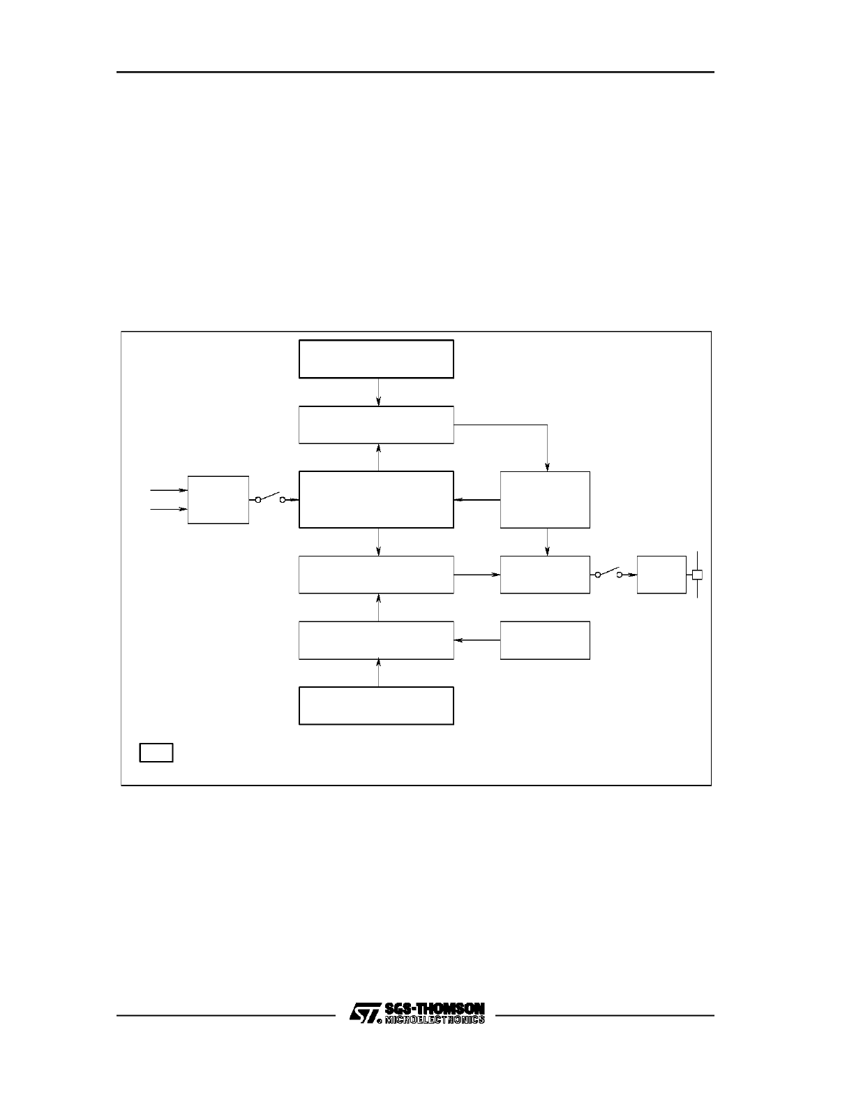
C167 FAMILY PRELIMINARY USER MANUAL
62/180
4.1
PWM-Channel
The Pulse Width Modulation Module consists of a block of 4 independant channels.
Each channel has a 16-bit up/down counter PTx, a 16-bit period register PPx, a 16-
bit pulse width register PWx with a shadow latch, two comparators, and the
necessary control logic. The operation of all four channels is controlled by two
common control registers, PWMCON0 and PWMCON1, and the interrupt control and
status is handled by one interrupt control register PWMIC, which is also common for
all channels.
Figure 13. PWM Channel Block Diagram
PPx Period Register
PWx Pulse Width Reg.
Comparator
Comparator
PTx
16-Bit Up/Down
Counter
Shadow Register
Output
Clear
Up/Down/
Control
Control
Write
Control
Control
Input
Match
Clock 1
Clock 2
POUTx
User Read-&
Writeable
VR001899
Match
Run
Enable
Note: For the following descriptions it is important to notice that the comparison of
the timer contents and the PWM value is performed through a ’greater than or equal
to’ comparison:
PWM Output Signal = [PTx] >= [PWx]

C167 FAMILY PRELIMINARY USER MANUAL
63/180
4.1.1 Operating Modes
Four different operating modes are available, described in the following sections.
Note: In these sections, the description and the associated figures state that the
respective PWM output pins POUTx are set on a match and reset on timer overflow,
etc. This is the default operation after reset. However, since the PWM output signals
are EXORed with the outputs of the respective port output latches, it is possible to
invert the PWM output signals by writing a ’1’ to the associated port output latch.
Please refer also to Chapter 11.7, Port 7.

C167 FAMILY PRELIMINARY USER MANUAL
64/180
Mode 0: Standard PWM Generation (Edge Aligned PWM)
In this mode, the PWM timer PTx is always counting up until the value in the period
register is reached. With the next count pulse, the timer is reset to 0000h, and starts
counting up again with the next count pulses. The PWM output signal is switched to a
high level when a match between the timer contents and the contents of the shadow
register is detected. The signal is switched back to a low level with the same signal
that clears the timer to 0000h. The period of the resulting PWM signal is the value of
the PPx register plus 1, counted in units of the timer resolution.
The duty cycle of the PWM output signal is controlled by the value in the pulse width
register PWx, respectively the value in the shadow register. This is true also for duty
cycles of 0% and 100%. For a PWM value of 0000h, the output will remain at a high
level, representing a duty cycle of 100%. For a PWM value higher than the value in
the period register, the output will remain at a low level, which corresponds to a duty
cycle of 0%.
Note that in this mode, the PWM value only affects the positive edge of the output
signal. The negative edge is always fixed and related to the clearing of the timer.
Therefore this mode is often referred to as Edge Aligned PWM.
Figure 14 illustrates the operation of a PWM channel in this mode, and shows
examples for different possible output waveforms. The period of the resulting PWM
signal is:
PWM
Period Mode 0
= [PPx] + 1
Note that in this mode, the distance from one negative signal edge to the next is
always equal to the period of the signal, also with changing duty cycles. The distance
of the center points of the high pulses, however, changes with changing duty cycles.
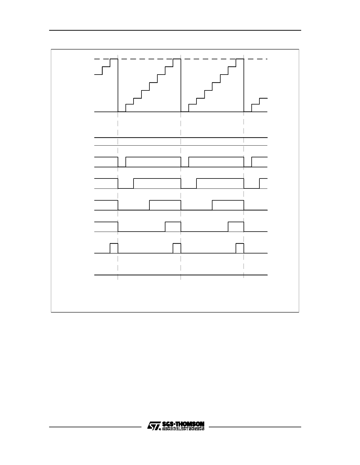
C167 FAMILY PRELIMINARY USER MANUAL
65/180
Figure 14. PWM Mode 0 Operation and Output Waveforms (Examples)
1
2
3
4
5
6
7
PPx
Period = 7
PTx Count
Value
0
7
6
0
7
6
5
4
3
2
1
0
1
PWx Pulse
Width=0
Duty Cycle
100%
PWx=1
PWx=2
87.5%
75%
25%
50%
PWx=6
PWx=4
PWx=7
12.5%
PWx=8
0%
LSR
Latch Shadow
Register;
Interrupt Request
LSR
LSR
VR001900

C167 FAMILY PRELIMINARY USER MANUAL
66/180
Mode 1: Symmetrical PWM Generation (Center Aligned PWM)
This mode is mainly intended to be used in electrical motor control applications. The
main characteristic of this mode is that when the PWM value is changed, both edges
of the output signal will be affected. This is achieved by the following operation:
The PWM timer is counting up from 0000h, until the value in the period register is
reached. With the next count pulse, the count direction is switched to count down, the
timer contents, however, will not be changed until the next count pulse, which
decrements the timer. The timer continues counting down until it reaches 0000h
again. The next count pulse will change the count direction again to count up, but will
not change the timer contents. With the following count pulse, the timer will increment
to 0001h, and the procedure described continues.
The PWM value, stored in the shadow register, is constantly compared to the timer
contents. When a match is found while the timer is counting up, the output signal is
switched to a high level. It remains on this high level, until the timer decrements again
to a value lower than that of the shadow register. In this way, both edges, the positive
and the negative edge of the signal, are controlled by the PWM value.
Figure 15 illustrates the operation of a PWM channel in this mode, and shows
examples for different possible output waveforms.
Note that in this mode, the period of the PWM signal is twice the period of the timer:
PWM
Period Mode 1
= 2
*
([PPx] + 1)
Note also that in this mode, the distance from the center point of a high pulse to the
center point of the next high pulse is always equal to the period of the signal, also
with changing duty cycles. Thus, this mode is often referred to as Center Aligned
PWM.
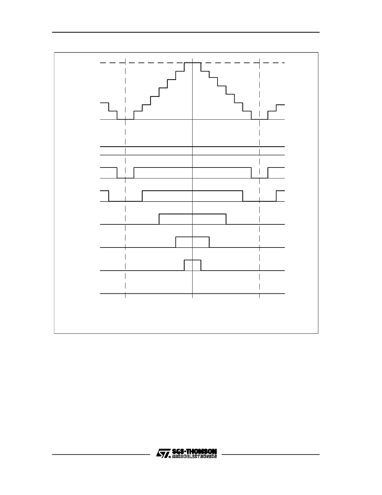
C167 FAMILY PRELIMINARY USER MANUAL
67/180
Figure 15. PWM Mode 1 Operation and Output Waveforms (Examples)
1
2
3
4
5
6
7
PPx
Period = 7
PTx Count
Value
0
0
1
PWx Pulse
Width=0
Duty Cycle
100%
PWx=1
PWx=2
87.5%
75%
25%
50%
PWx=6
PWx=4
PWx=7
12.5%
PWx=8
0%
LSR
Latch Shadow
Register;
Interrupt Request
Change Count
LSR
VR001901
1
0
1
2
3
4
5
6
7
0
Direction
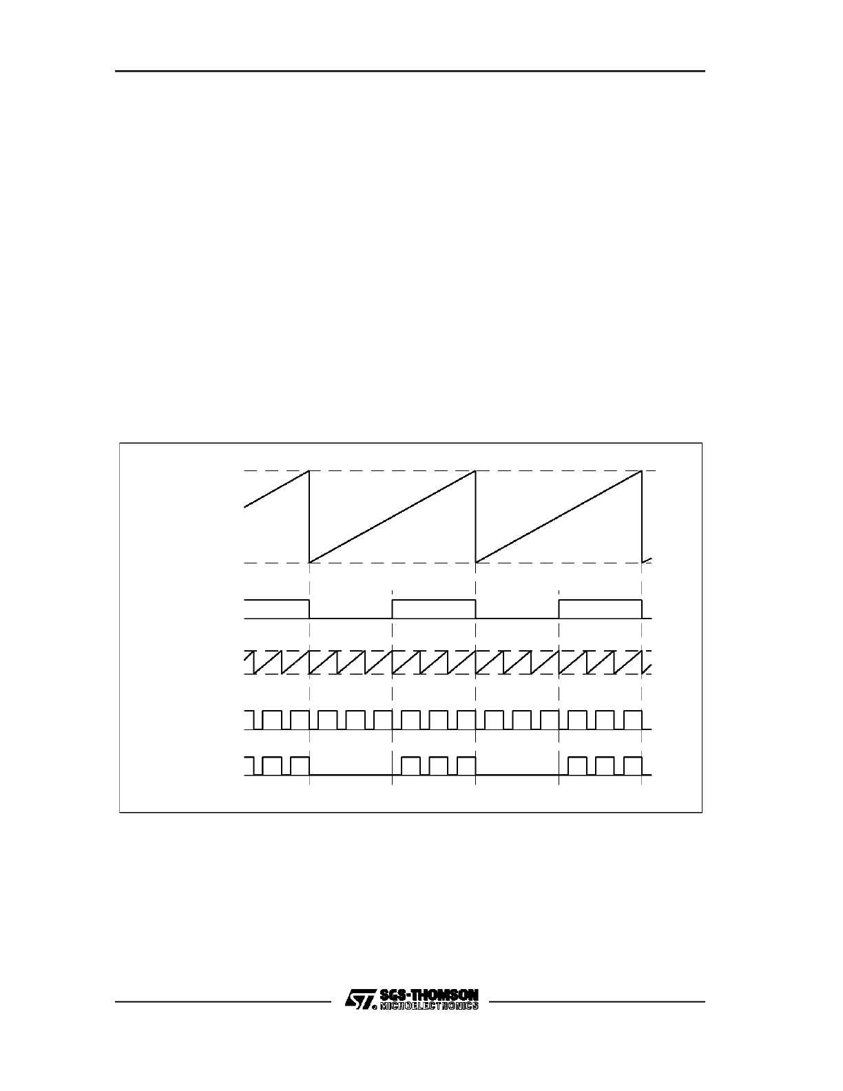
C167 FAMILY PRELIMINARY USER MANUAL
68/180
Burst Mode
This mode allows the combination of two PWM signals onto one output pin. This
mode is only possible for channels 0 and 1. When Burst Mode is selected through bit
PB01 in register PWMCON1, then the output signals of channel 0 and 1 are ANDed
together onto the pin associated with channel 0. The output of channel 1 can still be
used at its associated output pin (if the output is enabled). Figure 16 illustrates this
mode. Note that each of the two channels can either operate in mode 0 or 1, it is
recommended, however, to have both channels operating in the same mode when
using the burst mode.
Note that it is guaranteed by design, that no spurious spikes will occur at the output
pin of channel 0 in this mode. Instead, the signal will be transferred to the output pin
synchronously to internal clocks after the logical ANDing of channel 0 and channel 1.
Note that the EXORing of the alternate output function and the port output latch value
is done after the ANDing of channel 0 and 1.
Figure 16. PWM Pulse Burst Mode Operation (Example)
VR001902
PT0
Count
Value
Value
Period
PP0
Channel 1
PP1
Value
PP1 Count
POUT0
Output
Resulting
Channel 0

C167 FAMILY PRELIMINARY USER MANUAL
69/180
Single Shot Operation
This mode is available only for channels 2 and 3 of the PWM module. In this mode,
after the timer is started, the PWM channel will produce one single pulse (provided
the PWM value is between 0000h and the period value), and then the timer is
stopped by hardware, e.g. the run bit PTRx is reset to ’0’. In order to generate a
further pulse, the timer has to be started again through software by setting bit PTRx.
Figure 17 shows the single shot operation of one PWM channel.
Note that a retriggering of the output pulse is possible by software. When the pulse
has started (i.e. the output pin is set), then a write of the pulse width value into timer
PTx causes the output pulse to be extended by the specified pulse width. This
retriggering, also multiple retriggering, is always possible after the pulse has started
and before the timer has expired.
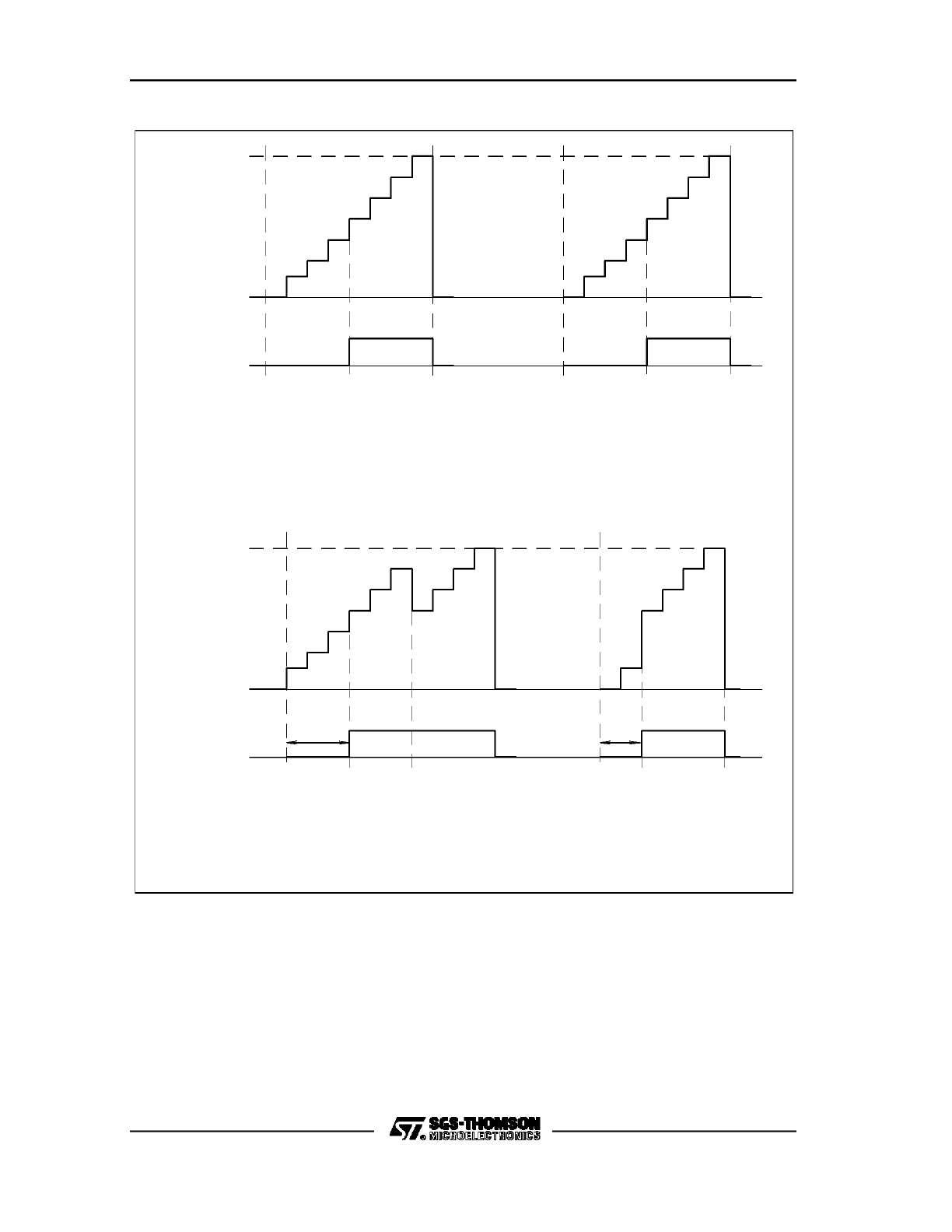
C167 FAMILY PRELIMINARY USER MANUAL
70/180
Figure 17. PWM Single Shot Mode Operation & Output Waveforms (Examples)
1
2
3
4
5
6
PPx
Period = 7
PTx Count
Value
0
7
0
7
6
5
4
3
2
1
Retrigger after Pulse
VR001903
0
0
Value
PTx Count
Period = 7
PPx
6
5
4
3
2
1
5
4
6
7
1
4
5
6
7
PWx Pulse
Width=4
has started: Write
PWx value to PTx
to PTx;
started: Write PWx value
Trigger before Pulse has
Shortens Delay Time t
D
D
t
t D
PWx Pulse
Width =4
Set PTRx by
Software
LSR;
PTRX Reset by
Hardware;
PTx stopped
Next Pulse
Software for
Set PTRx by
LSR
C167 FAMILY PRELIMINARY USER MANUAL
71/180
If a write of the pulse width value to the timer PTx occurs before the pulse has
started, the pulse will be started at that time point since the PTx and PWx contents
match.
By setting the period (PPx), the timer start value (PTx), and the pulse width value
(PWx) appropriately, the user has a wide variety of options to set the pulse width (tw)
and an optional pulse delay (td). Figure 17 illustrates some of these options.
Note: It is recommended to use the Single Shot Mode only together with Mode 0
(standard PWM generation).
4.1.2 PWM Module Registers
Figure 18 gives an overview of all Special Function Registers (SFRs) of the PWM
Module, while the following table lists their associated address. Note that some of
these registers, which are mostly only used once during the initialization, are moved
to the new extended SFR space, ESFR. When accessing these registers with ’REG’
or ’BITADDR’ addressing modes, an Extend Register (EXTR, EXTPR, EXTSR)
instruction is required.
Normal SFR Space
Extended ESFR Space
bitaddressable
non-bitaddressable
bitaddressable
non-bitaddressable
PWMCON0
PWMCON1
FF30h/98h
FF32h/99h
PW0
PW1
PW2
PW3
FE30h/18h
FE32h/19h
FE34h/1Ah
FE36h/1Bh
PWMIC
F17Eh/BFh
PT0
PT1
PT2
PT3
PP0
PP1
PP2
PP3
F030h/18h
F032h/19h
F034h/1Ah
F036h/1Bh
F038h/1Ch
F03Ah/1Dh
F03Ch/1Eh
F03Eh/1Fh
C167 FAMILY PRELIMINARY USER MANUAL
72/180
Figure 18. SFRs and Port Pins Associated with the PWM Unit
ODP7
Ports & Port Control Reg.
DP7
P7
POUT3...POUT0
P7.3...P7.0
PW1
PP1
PT1
PWMIC
PWMCON0
PWMCON1
VR001906
Alternate Functions
Data Registers
Control Registers
Interrupt Control
PW0
PP0
PT0
PT2
PP2
PW2
PT3
PP3
PW3
* Registers in Extended SFR Space
* ODP7
DP7
P7
* PT0..OT3
* PP0..PP3
PW0..PW3
PWMCON0
PWMCON1
* PWMIC
Port 7 Open Drain Control Register
Port 7 Direction Control Register
Port 7 Data Register
PWM Channel 0..3 Timer Register
PWM Channel 0..3 Period Register
PWM Channel 0..3 Pulse Width Register
PWM Control Register 0
PWM Control Register 1
PWM Interrupt Control Register
Up/Down Counter PTx
The counter PTx of a PWM channel is clocked by either the CPU clock or the CPU
clock divided by 64, selected through a respective control bit PTIx in the control
register PWMCON0. Thus, with a maximum CPU clock of 20 MHz, the resolutions
and frequencies listed in Table 4.1.2 can be achieved. The counter can be started or
stopped through the respective run control bit PTRx. In the Single Shot Mode, the
counter run bit PTRx of channels 2 and 3 is cleared by hardware when the timers
reach the value in the respective period register PPx. The counter can count up or
down, however, the count direction is controlled by hardware depending on the
selected operating mode; it can not be altered by software.

C167 FAMILY PRELIMINARY USER MANUAL
73/180
Table 4.1.2a:
PWM Unit Frequencies and Resolution in Mode 0 Operation
Resolution -->
Input Clock (@ 20 MHz)
8 Bit
10 Bit
12 Bit
14 Bit
16 Bit
CPU Clock
(50 ns Resolution)
78.13
KHz
19.53
KHz
4.88 KHz 1.22 KHz
305 Hz
CPU Clock / 64
(3.2 usec Resolution)
1.22 KHz
305 Hz
76.3 Hz
19.1 Hz
4.77 Hz
Table 4.1.2b:
PWM Unit Frequencies and Resolution in Mode 1 Operation
Resolution -->
Input Clock (@ 20 MHz)
8 Bit
10 Bit
12 Bit
14 Bit
16 Bit
CPU Clock
(50 ns Resolution)
39.1 KHz 9.77 KHz 2.44 KHz
610 Hz
152.6 Hz
CPU Clock / 64
(3.2 usec Resolution)
610 Hz
152.6 Hz
38.15 Hz
9.54 Hz
2.4 Hz
Note: The timer run bit PTRx only enables or disables the input clock to the timer, it
has no direct effect on the generation of the PWM signal. The timer is started through
setting bit PTRx, and it will continue counting until bit PTRx is reset. If bit PTRx is
cleared by software, the timer will stop when the instruction writes to the control
register PWMCON0, and the timer contents will remain at the last value. The PWM
output signal will then also remain at the level which was active at the time the timer
was stopped. If one wants to stop the generation of a PWM signal, there are several
different options. Since the PWM output signal is generated through a ’greater than
or equal to’ comparison between the timer contents and the contents of the PWx
register, respectively the shadow register (PWM Output Signal = PTx >= PWx), one
can force the output signal to a certain level through writing appropriate values either
to the PWx register or to the timer PTx itself. For example, writing the same or a
higher value (=< PPx) as contained in the shadow latch into the timer before the
PWM pulse has started results to an immediate setting of the PWM signal. Setting
the timer to a value lower than the one in the shadow latch will set the output to low.
To disable further PWM pulses, one can first stop the timer by clearing the run bit
PTRx. To abort a pulse in the single shot mode, one can set the timer to the same
value as in PPx. With the next clock pulse, the timer will be reset to 0, and stopped
through clearing bit PTRx by hardware. It is also important to note in this context, that
a write to PWx will immediately be copied into the shadow latch if bit PTRx is ’0’.
Note that is also possible to affect the PWM output signal through enabling/disabling
the output with the control bits PENx, or through changing the respective port latch
value.

C167 FAMILY PRELIMINARY USER MANUAL
74/180
Period Register PPx
The 16-bit period register PPx of a PWM channel is used to determine the period,
and thus the frequency, of the PWM signal. For this purpose, the contents of the
associated counter PTx is constantly compared to the contents of the period register
PPx. When a match is found between the two values, the counter is either reset to
0000h, or the count direction is switched from counting up to counting down,
depending on the selected operating mode of that PWM channel.
Pulse Width Register PWx
This 16-bit register holds the actual PWM value, which corresponds to the duty cycle
of the PWM signal. This register is connected to a 16-bit shadow register. The
operation of these two registers is as follows.
The contents of the shadow register are constantly compared to the contents of the
associated counter PTx. When the comparison shows that the timer contents are
greater than or equal to the contents of the shadow register, the PWM signal is set,
otherwise it is reset. This type of comparison allows a flexible control of the PWM
signal (see also the section on PTx).
The shadow register is loaded with the contents of the pulse width register PWx
depending on the following conditions:
a) When the counter PTx is not running (PTRx = 0), a write to register PWx writes to
both the pulse width register PWx and the shadow register of that channel. This is
used to initially load both registers.
b) When the counter is running, then in mode 0, the shadow register is loaded from
register PWx with the same signal that clears the counter PTx to 0000h (marked
with ’LSR’ in Figure 14). In mode 1, the shadow register is loaded when the count
direction of the counter is switched from down to up (marked with ’LSR’ in Figure
15).
PWM Control Register PWMCON0
This 16-bit control register controls the function of the timers of the four PWM
channels, and it holds the individual interrupt enable and request flags. The bits and
functions of this control register are shown hereafter. In order to modify the operation
of several channels with one instruction (e.g. bitfield instruction), the control bits are
organized into functional, not channel respective groups. This allows, for example, to
start or stop all 4 timers simultaneously with one bitfield instruction.

C167 FAMILY PRELIMINARY USER MANUAL
75/180
PWMCON0 (FF30h/98h)
PWM Module Control Register 0
Reset Value: 0000h
PIR0
PIE3
PIE2
PIE1
PIE0
15
14
13
12
11
10
9
8
0
1
2
3
4
5
6
7
PTI1
PTI0
PIR3
PIR2
PIR1
PTI3
PTI2
PTR1
PTR0
PTR3
PTR2
b15 = PIR3: PWM Channel 3 Individual Interrupt Request bit.
b14 = PIR2: PWM Channel 2 Individual Interrupt Request bit.
b13 = PIR1: PWM Channel 1 Individual Interrupt Request bit.
b12 = PIR0: PWM Channel 0 Individual Interrupt Request bit.
PIR0 = 0: No interrupt request
PIR0 = 1: Interrupt pending
b11 = PIE3: PWM Channel 3 Individual Interrupt Enable bit.
b10 = PIE2: PWM Channel 2 Individual Interrupt Enable bit.
b9 = PIE1: PWM Channel 1 Individual Interrupt Enable bit.
b8 = PIE0: PWM Channel 0 Individual Interrupt Enable bit.
PIE0 = 0: Individual Interrupt disabled
PIE0 = 1: Individual Interrupt enabled
b7 = PTI3: PWM Timer PT3 Input Clock Control bit.
b6 = PTI2: PWM Timer PT2 Input Clock Control bit.
b5 = PTI1: PWM Timer PT1 Input Clock Control bit.
b4 = PTI0: PWM Timer PT0 Input Clock Control bit.
PTI0 = 0: PT0 Input clock is CPU clock.
PTI0 = 1: PT0 input clock is CPU clock/256.
b3 = PTR3: PWM Timer PT3 Run Control bit.
b2 = PTR2: PWM Timer PT2 Run Control bit.
b1 = PTR1: PWM Timer PT1 Run Control bit.
b0 = PTR0: PWM Timer PT0 Run Control bit.
PTR0 = 0: PT0 stops.
PTR0 = 1: PT0 is running.
PWM Control Register PWMCON1
This register controls the modes of operation and the outputs of the PWM channels.
The mode of a channel, whether it operates in standard or symmetrical PWM mode
(edge or center aligned mode), is controlled by a mode bit, PMx. For channels 0 and
1, burst mode can be enabled/disabled by the control bit PB01. The single shot mode
of channels 2 and 3 is selected through bits PS2 and PS3, respectively. For each
PWM channel, one bit, PENx, controls whether the associated output pin is enabled
or not. If the output is not enabled, the respective pin can be used for general
C167 FAMILY PRELIMINARY USER MANUAL
76/180
purpose I/O, and the PWM signal can only be used to generate an interrupt request.
The register PWMCON1 is shown hereafter :
PWMCON1 (FF32h/99h)
PWM Module Control Register 1
Reset Value: 0000h
PB01
R
R
R
R
15
14
13
12
11
10
9
8
0
1
2
3
4
5
6
7
PM1
PM0
PIS3
PIS2
R
PM3
PM2
PEN1
PEN0
PEN3
PEN2
b15 = PS3: PWM Channel 3 Single shot Mode control bit.
b14 = PS2: PWM Channel 2 Single shot Mode control bit.
PS2 = 0: Normal operation.
PS2 = 1: Single shot operation.
b13 = R: Reserved.
b12 = PB01: PWM Channel 0 and 1 Burst Mode Control bit.
PB01 = 0: Normal operation of channels 0 an 1.
PB01 = 1: Outputs of channels 0 and 1 are ANDed onto POUT0.
b11 to b8 = R: Reserved.
b7 = PM3: PWM Channel 3 Mode Control bit.
b6 = PM2: PWM Channel 2 Mode Control bit.
b5 = PM1: PWM Channel 1 Mode Control bit.
b4 = PM0: PWM Channel 0 Mode Control bit.
PM0 = 0: Mode 0 operation.
PM0 = 1: Mode 1 operation.
b3 = PEN3: PWM Channel 3 Output Enable control bit.
b2 = PEN2: PWM Channel 2 Output Enable control bit.
b1 = PEN1: PWM Channel 1 Output Enable control bit.
b0 = PEN0: PWM Channel 0 Output Enable control bit.
PEN0 = 0: Output POUT0 disabled.
PEN0 = 1: Output POUT0 enabled.
4.1.3 Interrupt Request Generation
Each of the four channels of the PWM Module can generate an interrupt request
(furthermore referred to as ’channel interrupt’), however, only one interrupt vector is
assigned to all four channels (furthermore referred to as ’module interrupt’). To
distinguish between the channel interrupts, register PWMCON0 has individual
interrupt enable and interrupt request flags for each channel. When the individual
enable flag PIEx of a channel is set, then the interrupt request flag PIRx of that

C167 FAMILY PRELIMINARY USER MANUAL
77/180
channel is set with the same signal that loads the shadow register with the value from
register PWx (see signal ’LSR’ in Figures 4.1-2 and 4.1-3). This indicates that the
newest PWM value was transferred to the shadow latch for being compared to the
timer contents, and that register PWx is now ’empty’ to receive the next value.
The module interrupt for all four channels is controlled by the PWM Module Interrupt
Control register PWMIC. This register is organized like any other standard interrupt
control register, shown hereafter. If the module interrupt enable bit PWMIE is set,
then the interrupt request flag PWMIR is set if any of the channel interrupt request
flags PIRx is set (provided this interrupt is enabled through the respective PIEx bit).
Software is used to then poll the channel interrupt request flags to determine which
channel(s) caused the interrupt.
PWMIC (F17Eh/BFh)
PWM Module Interrupt Control Register
Reset Value: 0000h
0
1
2
3
4
5
6
7
PWMIR
PWMIE
GLVL
ILVL
b7 = PWMIR: PWM Module Interrupt Request Flag.
PWMIR = 0: No interrupt request.
PWMIR = 1: Interrupt request.
b6 = PWMIE: PWM Module Interrupt Enable control bit.
PWMIE = 0: Interrupt disabled.
PWMIE = 1: Interrupt enabled.
b5 to b2 = ILVL: PWM Module Interrupt Priority Level.
ILVL = Fh: Highest priority level.
ILVL = 0: Lowest priority level.
b1, b0 = GLVL: PWM Module Interrupt Group Priority.
GLVL = 3: Highest group priority.
GLVL = 0: Lowest group priority.
Note that the channel interrupt request flags (in register PWMCON0) will not be
automatically cleared by hardware when the interrupt service routine is vectored to;
they must be cleared by software. The module interrupt request flag PWMIR is
cleared by hardware when the service routine is vectored to, regardless whether the
interrupt was caused by one or several channels. However, it will be set again if
during execution of the service routine a new channel interrupt request is generated.
C167 FAMILY PRELIMINARY USER MANUAL
78/180
4.1.4 PWM Output Signals
In the C167, the output signals of the four PWM channels are connected as alternate
output functions to four pins of Port 7. For each of the four channels, an individual
output enable control bit PENx is available in control register PWMCON1. The
following table shows the reference between the PWM output signals and the
associated port pins:
Port Pin
PWM Alternate Function
P7.0
POUT0PWM Channel 0 Output
P7.1
POUT1PWM Channel 1 Output
P7.2
POUT2PWM Channel 2 Output
P7.3
POUT3PWM Channel 3 Output
Different to other alternate output functions, the PWM signals are EXORed with the
respective port latch outputs (see Chapter 11.7). In this way, it is possible to select
whether the PWM signal is inverted at the output or not. If the port latch is ’0’ (default
after reset), the associated PWM signal is not inverted, the output signal is as shown
in Figures 14 to 17. If the port latch is ’1’, the PWM signal is inverted.
It is interesting to note that in the C167, Port 7 has additional open drain control. This
feature can be used to combine two or more PWM outputs through a Wired-AND
configuration, using an external pullup device. In this way, it is possible, for example,
to have any channels to operate in a burst mode, besides the implemented burst
mode for channels 0 and 1.

C167 FAMILY PRELIMINARY USER MANUAL
79/180
5.
SECOND CAPTURE/COMPARE UNIT, CAPCOM2
In the C167, the entire CAPCOM Unit known from the ST10x166 will be implemented
twice. In the following, the two units will be referred to as CAPCOM1 (the unit known
from the ST10x166) and CAPCOM2. The CAPCOM2 unit gives the user two extra
timers, and 16 extra capture/compare registers. The new CAPCOM2 Unit is shown in
Figure 19.
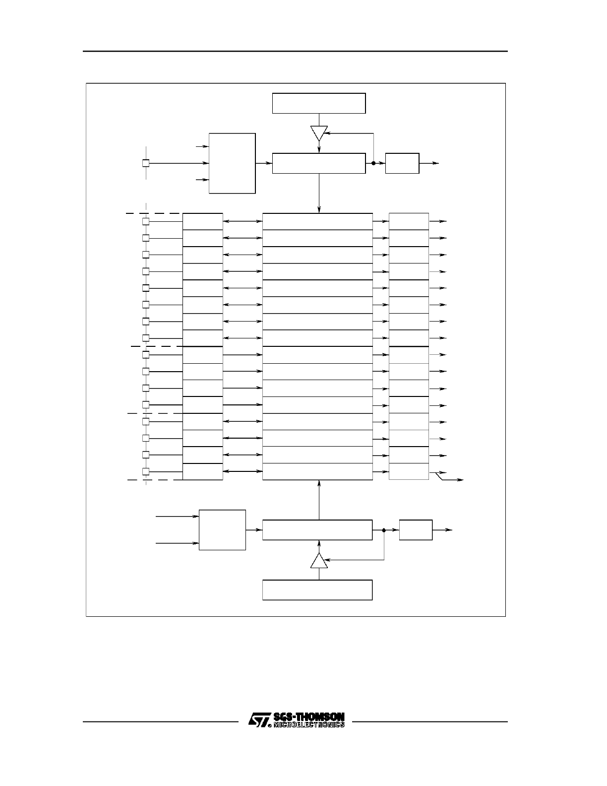
C167 FAMILY PRELIMINARY USER MANUAL
80/180
Figure 19. CAPCOM2 Unit Block Diagram
Reload Reg. T7REL
CAPCOM2 Timer T7
Input
Control
T7IR
Capt./Comp.Reg.CC16
Interrupt
P8.0
P8.1
P8.2
P8.3
P8.4
P8.5
P8.6
P8.7
P1H.4
P1H.5
P1H.6
P1H.7
P7.4
P7.5
P7.6
P7.7
PORT 8
PORT 1
PORT 7
Interrupt
Request
System
Clock
Timer T6
GPT2
P2.15
T7IN
CC15IO
CC31IR
CC30IR
CC29IR
CC28IR
CC27IR
CC26IR
CC25IR
CC24IR
CC23IR
CC22IR
CC21IR
CC20IR
CC19IR
CC18IR
CC17IR
CC16IR
Requests
Trigger A/D
Channel
Injection
System
Clock
Input
Control
CAPCOM Timer T8
T8IR
GPT2
Timer T6
Reload Register T8REL
Request
Interrupt
CC17
CC18
CC19
CC20
CC21
CC22
CC23
CC24
CC25
CC26
CC27
CC28
CC29
CC30
Capt./Comp. Reg.CC31
VR001904
C167 FAMILY PRELIMINARY USER MANUAL
81/180
The two new timers will be named T7 and T8, and the associated reload registers are
T7REL and T8REL, respectively. The control register for these timers is T78CON.
The sixteen additional compare registers will be CC16 through CC31. Four additional
registers CCM4 through CCM7 control the operating modes of registers CC16
through CC31. The CAPCOM2 unit will use the pins of Port 8, four pins of Port 1, and
four pins of Port 7 for the alternate capture input/compare output functions (see also
Chapter 11).
Figure 20 gives an overview on all the Special Function Registers (SFRs) related to
the CAPCOM2 Unit, while the following table lists their associated address. Note that
some of these registers, which are mostly only used once during the initialization, are
moved to the new extended SFR space, ESFR. When accessing these registers with
’REG’ or ’BITADDR’ addressing modes, an Extend Register (EXTR, EXTPR, EXTSR)
instruction is required.
Normal SFR Space
Extended ESFR Space
bitaddressable
non-bitaddressable
bitaddressable
non-bitaddressable
CCM4
CCM5
CCM6
CCM7
T78CON
FF22h/91h
FF24h/92h
FF26h/93h
FF28h/94h
FF20h/90h
CC16
CC17
CC18
CC19
CC20
CC21
CC22
CC23
CC24
CC25
CC26
CC27
CC28
CC29
CC30
CC31
FE60h/30h
FE62h/31h
FE64h/32h
FE66h/33h
FE68h/34h
FE6Ah/35h
FE6Ch/36h
FE6Eh/37h
FE70h/38h
FE72h/39h
FE74h/3Ah
FE76h/3Bh
FE78h/3Ch
FE7Ah/3Dh
FE7Ch/3Eh
FE7Eh/3Fh
CC16IC
CC17IC
CC18IC
CC19IC
CC20IC
CC21IC
CC22IC
CC23IC
CC24IC
CC25IC
CC26IC
CC27IC
CC28IC
CC29IC
CC30IC
CC31IC
T7IC
T8IC
F160h/B0h
F162h/B1h
F164h/B2h
F166h/B3h
F168h/B4h
F16Ah/B5h
F16Ch/B6h
F16Eh/B7h
F170h/B8h
F172h/B9h
F174h/BAh
F176h/BBh
F178h/BCh
F184h/C2h
F18Ch/C6h
F194h/CAh
F17Ah/BDh
F17Ch/BEh
T7
T8
T7REL
T8REL
F050h/28h
F052h/29h
F054h/2Ah
F056h/2Bh
C167 FAMILY PRELIMINARY USER MANUAL
82/180
Figure 20. SFRs and Port Pins Associated with the CAPCOM2 Unit
ODP2
Ports & Direction Control
DP2
P2
T7IN/CC15IO
P2.15
P8.0...P8.7
CC16IO...CC23IO
P8
DP8
ODP8
T7
T7REL
T8REL
T8
CC16
CC17
CC18
CC19
T7IC
T78CON
T8IC
CCM4
CC19IC
CC18IC
CC17IC
CC16IC
DP1H
P1H
ODP7
DP7
P7
CC28IO...CC31IO
P7.4...P7.7
CC24IO...CC27IO
P1H.4...P1H.7
CC23
CC22
CC21
CC20
CCM5
CC20IC
CC21IC
CC22IC
CC23IC
CC24
CC25
CC26
CC27
CCM6
CC27IC
CC26IC
CC25IC
CC24IC
CC31
CC30
CC29
CC28
CCM7
CC28IC
CC29IC
CC30IC
CC31IC
VR001905
Alternate Functions
Data Registers
Control Registers
Interrupt Control
* Registers in Extended SFR Space
* DP1H
Port 1 High Byte Direction Ctl.
P1H
Port 1 High Byte Data Reg.
* ODP2
Port 2 Open Drain Control Reg.
DP2
Port 2 Direction Control Reg.
P2
Port 2 Data Reg.
* ODP7
Port 7 Open Drain Control Reg.
DP7
Port 7 Direction Control Reg.
P7
Port 7 Data Reg.
* ODP8
Port 8 Open Drain Control Reg.
DP8
Port 8 Direction Control Reg.
P8
Port 8 Data Reg.
* T7
* T7REL
* T8
* T8REL
T78CON
CC16..CC31
CCM4..CCM7
* T7IC
* T8IC
CC16IC..CC31IC
CAPCOM Timer 7 & 8 Control
CAPCOM Timer 7 Register
CAPCOM Timer 7 Reload Reg.
CAPCOM TImer 8 Register
CAPCOM Timer 8 Reload Reg.
CAPCOM Registers CC16..31
CAPCOM Mode Control Reg. 4..7
CAPCOM Timer 7 Interrupt Control
CAPCOM Timer 8 Interrupt Control
CAPCOM Reg. CC16..31 Int. Control

C167 FAMILY PRELIMINARY USER MANUAL
83/180
In the C167, when using the CAPCOM2 unit, some differences compared to the
known CAPCOM1 unit have to be taken into account, described in the following
section. Besides these exceptions, all the functions and operation of the CAPCOM1
Unit described in the ST10 User Manual also refer to the CAPCOM2 Unit, in a
respective manner.
a) Timer T7 has no separate count input (comparable to T0IN for timer T0). Instead,
when selected for counter operation, T7 will use the pin P2.15/CC15IO as a count
input. P2.15 can either be used as general purpose I/O pin, or for capture input, or
for compare output. With this, the user has several options: Counter T7 can either
be clocked by software toggling or by compare output signals of pin P2.15; an
external clock pulse for T7 can be used to trigger an interrupt request (CC15INT),
and additionally a capture of either T0 or T1 contents can be performed. It is also
possible to provide the same external count events for both CAPCOM units by
externally connecting the signal to both inputs, T0IN and CC15IO. In this way, T0
and T7 count synchronously the same external event, with an optional capture
and interrupt request for this count event. Figure 21 shows both CAPCOM units,
and a configuration example for synchronous operation. Since in this example T0
and T7 are clocked by the same event, the two timers can be regarded as one
timer, having access to all 32 capture/compare registers. In a similar manner, T1
and T8 can be clocked with the same internal clock (or GPT2 timer T6 clock), and
they can be regarded in this case as one timer, having also access to all 32
registers. However, since it is not possible to start both timers with one instruction,
a slight time delay may be possible.
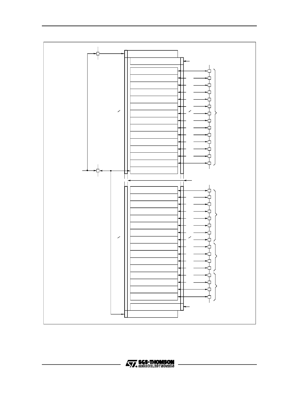
C167 FAMILY PRELIMINARY USER MANUAL
84/180
Figure 21. CAPCOM1/CAPCOM2 Configuration Example
CC0
CC1
CC2
CC3
CC4
CC5
CC7
CC8
CC9
CC10
CC11
CC12
CC13
CC14
CC15
VR0A1904
C
a
p
t
u
r
e
C
o
m
p
a
r
e
T1
T0
e
r
a
p
m
o
C
e
r
u
t
p
a
C
T1
T0
CPU
/y
CC16
C
a
p
t
u
r
e
C
o
m
p
a
r
e
T7
T8
e
r
a
p
m
o
C
e
r
u
t
p
a
C
CC31
CC30
CC29
CC28
CC27
CC26
CC25
CC24
CC23
CC22
CC21
CC20
CC19
CC18
CC17
T8
T7
/x
PORT P2
PORT P8
PORT P1H
PORT P7
T0IN
CC15IO
External
Connection
Signal
External
See Description
Internal
Connection
Clock
Clock
CPU

C167 FAMILY PRELIMINARY USER MANUAL
85/180
b) CAPCOM2 registers CC24 through CC27 only have external input pins, as an
alternate function at Port P1H. This means, that only external capture inputs can
be used, it is not possible to use these pins for compare output. However, these
registers can still be used in the ’interrupt only’ compare modes, to generate
interrupt requests at predefined events.

C167 FAMILY PRELIMINARY USER MANUAL
86/180

C167 FAMILY PRELIMINARY USER MANUAL
87/180
6.
ASYNCHRONOUS/SYNCHRONOUS SERIAL INTERFACE
6.1
Even / Odd Parity Selection
The serial interface ASC0 of the C167 will have one enhancement compared to the
respective interfaces in the ST10x166. For the parity, now a selection for even or odd
parity generation/check will be available.
When an asynchronous mode with parity is enabled, a new control bit, S0ODD
(S0CON.12), selects between even and odd parity generation/check. The default
after reset, S0ODD = 0, selects even parity (as in the ST10x166). Hereafter is the
ASC0 control register S0CON.
S0ODD = 0:
Even parity:
If the data contains an even number of ’1s’, then the parity bit = 0
If the data contains an odd number of ’1s’, then the parity bit = 1
S0ODD = 1:
Odd parity:
If the data contains an even number of ’1s’, then the parity bit = 1
If the data contains an odd number of ’1s’, then the parity bit = 0
S0CON (FFB0h/D8h)
Serial Channel Control Register
Reset Value: 0000h
S0ODD
R
S0OE
S0FE
S0PE
15
14
13
12
11
10
9
8
0
1
2
3
4
5
6
7
S0PEN
S0REN
S0R
S0LB
S0BRS
S0OEN
S0FEN
S0M
S0STP
b15 = S0R: Baud Rate Generator Run bit.
S0R = 0: Baud rate generator disabled.
S0R = 1: Baud rate generator enabled.
b14 = S0LB: Loop Back Mode Enable bit.
S0LB = 0: Loop back mode disabled.
S0LB = 1: Loop back mode enabled.
b13 = S0BRS: Baud Rate Selection bit.
S0BRS = 0: Baud rate factor is 1.
S0BRS = 1: Baud rate factor is 2/3.
b12 = S0ODD: Even / Odd Parity Selection.

C167 FAMILY PRELIMINARY USER MANUAL
88/180
S0ODD = 0: Even parity.
If the data contains an even number of ”1” then parity bit = 0
S0ODD = 1: Odd parity.
If the data contains an even number of ”1” then parity bit = 1
b11 = R: Reserved.
b10 = S0OE: Overrun Error Flag.
Set by hardware when an overrun error occurs and S0OEN = 1.
Must be reset by software.
b9 = S0FE: Framing Error Flag.
Set by hardware when a framing error occurs and S0FEN = 1.
Must be reset by software.
b8 = S0PE: Parity Error Flag.
Set by hardware when a parity error occurs and S0PEN = 1.
Must be reset by software.
b7 = S0OEN: Overrun Check Enable bit.
S0OEN = 0: Overrun check disabled.
S0OEN = 1: Overrun check enabled.
b6 = S0FEN: Framing Check Enable bit.
S0FEN = 0: Framing check disabled.
S0FEN = 1: Framing check enabled.
b5 = S0PEN: Parity Check Enable bit.
S0PEN = 0: Parity check disabled.
S0PEN = 1: Parity check enabled.
b4 = S0REN: Receiver Enable bit.
Used to initiate reception.
Reset by hardware after a byte in synchronous mode has been received.
S0REN = 0: Receiver disabled.
S0REN = 1: Receiver enabled.
b3 = S0STP: Number of Stop Bits Selection.
S0STP = 0: One stop bit.
S0STP = 1: Two stop bits.
b2 to b0 = S0M: ASC0 Mode Control.
6.2
Double Buffered Transmit
An additional buffer register is implemented for the transmit buffer S0TBUF in the
asynchronous/synchronous serial interface ASC0. This allows a double buffered
transmission, that is, while a transmission is in progress, the next data to be
transmitted can already be loaded into the transmit buffer S0TBUF. In this way, it is
possible to perform continuous transmissions without any gaps other than the
programmed number of stop bits between two consecutive transmissions.
An additional interrupt source and vector will be implemented in order to flag the
condition that the transmit buffer is empty and ready to be loaded with the next data.

C167 FAMILY PRELIMINARY USER MANUAL
89/180
The Transmit Buffer Empty interrupt is controlled through register S0TBIC (see
Chapter 10).
The operation of the buffered transmission is as follows : the data to be transferred is
written into the transmit buffer S0TBUF. If the transmit shift register is empty, i.e. no
transmission is currently in progress, the contents of the S0TBUF will be copied into
the transmit shift register, and the transmission will be started. At the same time, the
transmit buffer empty interrupt request flag S0TBIR will be set. Now the text data to
be transmitted can be loaded into S0TBUF. An internal flag is used to indicate that
the transmit buffer is full, i.e. has been written to. Directly, before the last stop bit of
the current transmission is sent out, the transmit complete interrupt request flag
S0TIR will be set to indicate that a data frame has been sent out. When the transmit
buffer S0TBUF is full, its data is transferred into the transmit shift register, and the
transmit buffer empty interrupt request S0TBIR is set.
In this way, there are two informations flagged to the user through two different
interrupt requests : the transmit buffer empty interrupt S0TBINT indicates that the
transmit buffer S0TBUF is ready to be loaded with the next data to be transmitted,
while the transmit complete interrupt S0TINT indicates that a transmission of a data
frame has been finished.
The great advantage of this double buffering transmit is that for continuous
transmissions, the time frame available for loading the next data into the transmit
buffer is the time required for the transmission of one complete data frame. Without
this feature, the next data frame must be loaded within the time required to sent out
the last stop bit of the previous data frame.

C167 FAMILY PRELIMINARY USER MANUAL
90/180

C167 FAMILY PRELIMINARY USER MANUAL
91/180
7.
SYNCHRONOUS SERIAL CHANNEL, SSC
In addition to the asynchronous/synchronous serial interface ASC0, the C167 has a
dedicated high-speed Synchronous Serial Channel, the SSC. This interface provides
the same synchronous mode as the ASC0, and is also compatible to the popular SPI
interface. It can be used for simple I/O expansion via shift registers, for connection of
a variety of peripheral components, such as A/D converters, EEPROMs, etc., or for
allowing several microcontrollers to be interconnected in a master/slave or
multimaster configuration. It supports full-duplex or half-duplex operation, and can
run in a master or a slave mode.
7.1
SSC Block Diagram
Figure 22 shows a rough block diagram of the SSC. The central element of the SSC
is a shift register, which is configurable in length from 2 to 16 bits. The input and the
output of this shift register are each connected via a control logic to a pin,
P3.9/MTSR
(Master
Transmit/Slave
Receive)
and
P3.8/MRST
(Master
Receive/Slave Transmit). This shift register can be written to through a Transmit
Buffer Register SSCTB, and can be read through a Receive Buffer Register SSCRB.
C167 FAMILY PRELIMINARY USER MANUAL
92/180
Figure 22. Synchronous Serial Channel SSC Block Diagram
VR001886
Receive Int. Request
Transmit Buffer
Register SSCTB
Internal Bus
SSCRB
Receive Buffer
16-Bit Shift Register
Control
Pin
MTSR
MRST
P3.8
P3.9
SSC Control Block
Status
Control
Transmit Int. Request
Error Int. Request
Clock
Control
Baud Rate
Generator
CPU
Clock
SCLK
Slave Clock
Master Clock
P3.13
As the SSC is a synchronous serial interface, for each transfer a separate clock
signal must be provided. The SSC has implemented a full featured clock control
circuit, which can generate the clock via a 16-bit baud rate generator in the master
mode, or receive the transfer clock in the slave mode. The clock signal is fully
programmable for clock polarity and phase. The pin used for the clock signal is
P3.13/SCLK.
The SSC control block is responsible for controlling the different modes and
operation of the SSC, checking the status, and generating the respective interrupt
signals, one for transmit, one for receive, and one for possible error conditions.

C167 FAMILY PRELIMINARY USER MANUAL
93/180
7.2
General Operation of the SSC
After initialisation of the SSC, the data to be transmitted is written into the transmit
buffer register SSCTB. If no transfer is currently in progress, the contents of SSCTB
is immediately copied into the shift register. In master mode, this will initiate the
transfer, in slave mode the transfer is started through an external clock signal. When
the transfer is started, the busy flag, SSCBSY, is set, and the transmit interrupt
request flag SSCTIR will be generated. This indicates that the transmit buffer now is
empty, and the next transmit data can already be written into register SSCTB. While
the transmit data in the shift register is shifted out bit per bit, the incoming receive
data are shifted in, synchronized with the clock signal at pin SCLK. When the
preprogrammed number of bits are shifted out (the same number is shifted in), the
contents of the shift register is transferred to the receive buffer register SSCRB, and
the receive interrupt request flag SSCRIR is generated. If no further transfer is to
take place, the busy flag SSCBSY will be reset by hardware at the same time.
C167 FAMILY PRELIMINARY USER MANUAL
94/180
7.3
SSC Control, Status and Data Registers
Figure 23 gives an overview of the SFRs and port pins associated with the SSC.
Figure 23. SFRs and Port Pins Associated with the Synchronous Serial
Channel
ODP3
Ports & Direction Control
DP3
P3
MTSR P3.9
MRST P3.8
VR001908
Alternate Functions
Data Registers
Control Registers
Interrupt Control
SSCEIC
SSCRIC
SSCTIC
* Registers in Extended SFR Space
SSCBR
SSCCON
SSCTB
SSCRB
SCLK P3.13
* ODP3
DP3
P3
* SSCBR
* SSCTB
* SSCRB
SSCCON
SSCTIC
SSCRIC
SSCEIC
Port 3 Open Drain Control Register
Port 3 Direction Control Register
Port 3 Data Register
Synchronous Serial Channel Baud Rate Register
Synchronous Serial Channel Transmit Buffer Register
Synchronous Serial Channel Receive Buffer Register
Synchronous Serial Channel Control Register
Synchronous Serial Channel Transmit Interrupt Control Register
Synchronous Serial Channel Receive Interrupt Control Register
Synchronous Serial Channel Error Interrupt Control Register
7.3.1 SSC Control Register SSCCON
Hereafter are shown the bits and functions of the SSC Control Register SSCCON.
From a programming point of view, SSCCON is partly divided into two registers,
located to the same physical address. The upper two bits, SSCEN and SSCMS, are
always available. An access to bits 13..0 addresses two different registers,
depending on the state of the SSC enable bit, SSCEN. When the SSC is disabled
with SSCEN = 0, the bits which control the basic operation of the SSC are available
for initialisation. After enabling the SSC with setting SSCEN to ’1’, an access to
SSCCON[13..0] returns status information, such as the busy and the error flags,
which are necessary during the operation of the SSC. The partitioning of register
SSCCON is illustrated by showing the register twice. The first register represents the
function and symbols of the bits while SSCEN = 0, while the second register
represents the function and symbols with SSCEN = 1.

C167 FAMILY PRELIMINARY USER MANUAL
95/180
Care should be taken when accessing the SSCCON register, and the partitioning of
this register should always be kept in mind. When SSCEN = 0, bits 7, 12 and 13 of
register SSCCON are not defined and should be set to ’0’. With SSCEN = 1, bits 4
through 7, and bit 13 of SSCCON are reserved and should be set to ’0’. This has to
be taken into account when accessing register SSCCON via Read-Modify-Write
instructions, such as BSET, BCLR, AND/OR/XOR, BFLDL/H, etc. In the following,
the individual bits and bit fields of the SSCCON are discussed.
SSCCON (FFB2/D9)
Synchronous Serial Channel Control Register
Reset Value: 0000h
SSCBSY
SSCBEN
15
14
13
12
11
10
9
8
0
1
2
3
4
5
6
7
SSCPH
SSCHB
SSCEN
SSCMS
R
R
SSCPO
SSCBE
SSCPEN
SSCPE
SSCREN
SSCRE
SSCTEN
SSCTE
SSCBM
SSCBC
b15 = SSCEN: Synchronous Serial Channel Enable control bit.
b14 = SSCMS: SSC Master Select bit.
b13 = R: Reserved.
b12 = SSCBSY: SSC Busy Flag.
If SSCEN = 1.
b11 = SSCBEN, if SSCEN = 0: SSC Baudrate Error Enable control bit.
SSCBE,
if SSCEN = 1: SSC Baudrate Error Indication Flag.
b10 = SSCPEN, if SSCEN = 0: SSC Phase Error Enable control bit.
SSCPE,
if SSCEN = 1: SSC Phase Error Indication Flag.
b9 = SSCREN, if SSCEN = 0: SSC Receive Error Enable control bit.
SSCRE,
if SSCEN = 1: SSC Receive Error Indication Flag.
b8 =
SSCTEN, if SSCEN = 0: SSC Transmit Error Enable control bit.
SSCTE,
if SSCEN = 1: SSC Receive Error Indication Flag.
b7 = R: Reserved.
b6 =
SSCPO,
if SSCEN = 0: SSC Clock Parity control bit.
b5 =
SSCPH,
if SSCEN = 0: SSC Clock Phase control bit.
b4 =
SSCHB,
if SSCEN = 0: SSC Heading control bit.
b3 to b0 = SSCBM,
if SSCEN = 0: SSC Data Width Selection bit field.
SSCBC,
if SSCEN = 1: SSC bit Count Field.

C167 FAMILY PRELIMINARY USER MANUAL
96/180
Enable/Disable Control
Bit SSCEN globally enables or disables the synchronous serial interface. Setting
SSCEN to ’0’ stops the baud rate generator and all internal activities of the SSC.
Current transfers are aborted. The alternate output functions at pins P3.8/MRST,
P3.9/MTSR, and P3.13/SCLK return to their disable state, which is a logic high.
These pins can now be used for general purpose I/O. Special care should be taken
with pin P3.13/SCLK when operating with a clock polarity SSCPO = 0 (detailled in
Chapter 7.4.1).
When SSCEN = 0 (default after reset), register SSCCON provides the bits used to
control the operation of the SSC. When SSCEN = 1, any access to register SSCCON
returns the status flags. The selection, which part of the SSCCON register is
accessed, is done according to the state of SSCEN valid before the current access.
That means, when SSCEN = 0, register SSCCON can be written to with one
instruction initializing the control bits and setting bit SSCEN to ’1’, for example,
MOV SSCCON,#0C057h. The new state of SSCEN becomes valid after this
instruction. The same operation is true when SSCEN is ’1’: An instruction which
resets SSCEN to ’0’ would write bits 0..13 into the flag portion of register SSCCON,
since the previous state of SSCEN was ’1’. Since the flags are modified by hardware,
it is strongly recommended to avoid Read-Modify-Write instructions on register
SSCCON while SSCEN = 1. To disable the SSC, for example to select a different
data width, use a MOV SSCCON,#0 instruction to clear the SSCEN bit.
Master or Slave Operation
Other than the synchronous mode of the ASC0, which can only operate as a master
interface, the SSC can operate either in master or in slave mode. This operation is
selected through the Master Select Bit, SSCMS. In the master mode, SSCMS = 1,
the SSC of the C167 generates and outputs the clock at pin P3.13/SCLK, and
initiates data transfers. All other devices connected to the serial bus must be in slave
mode, receiving the shift clock, and only responding to transfers.
In the slave mode, SSCMS = 0 (default after reset), the shift clock is received
through pin P3.13/SCLK. The SSC can only respond to transfers initiated by another
master connected to the serial bus, it is not possible in this mode to initiate a data
transfer. The master/slave modes are discussed in more detail in Chapter 7.4.

C167 FAMILY PRELIMINARY USER MANUAL
97/180
Selecting Transfer Data Width and Shift Direction
The SSC in the C167 is not dedicated to a certain data width, for instance only a byte
or a word transfer. Instead, the data width can be programmed to be any number
between two and sixteen bits. The 4-bit field SSCBM determines the transfer data
width, according to the following table:
SSCBM
Transfer
Data Width
SSCBM
Transfer
Data Width
0000
0001
0010
0011
0100
0101
0110
0111
reserved
2 Bit
3 Bit
4 Bit
5 Bit
6 Bit
7 Bit
8 Bit
1000
1001
1010
1011
1100
1101
1110
1111
9 Bit
10 Bit
11 Bit
12 Bit
13 Bit
14 Bit
15 Bit
16 Bit
Bit 4, SSCHB (Heading Bit Control), of register SSCCON determines whether the
LSB (least significant bit) or the MSB (most significant bit) of the data is the first
transmitted bit. With SSCHB = 0, the LSB will be shifted first. This mode is required
by the synchronous mode of the ASC0 in the C167 (and also the synchronous
modes of ASC0/ASC1 of the ST10x166 family, and the serial ports of the 8051
family). Serial interfaces operating compatible to the SPI mode, however, require the
MSB to be the first transmitted bit. In this case, SSCHB must be set to ’1’.
Regardless which data width is selected, and whether the MSB or the LSB is
transmitted first, the transfer data is always right aligned in registers SSCTB and
SSCRB, with the LSB of the transfer data at the LSB position of these registers, i.e.
bit 0. The internal logic at the shift register totally takes care of correctly performing
the selected operation. Examples for this feature are shown in Figure 24.
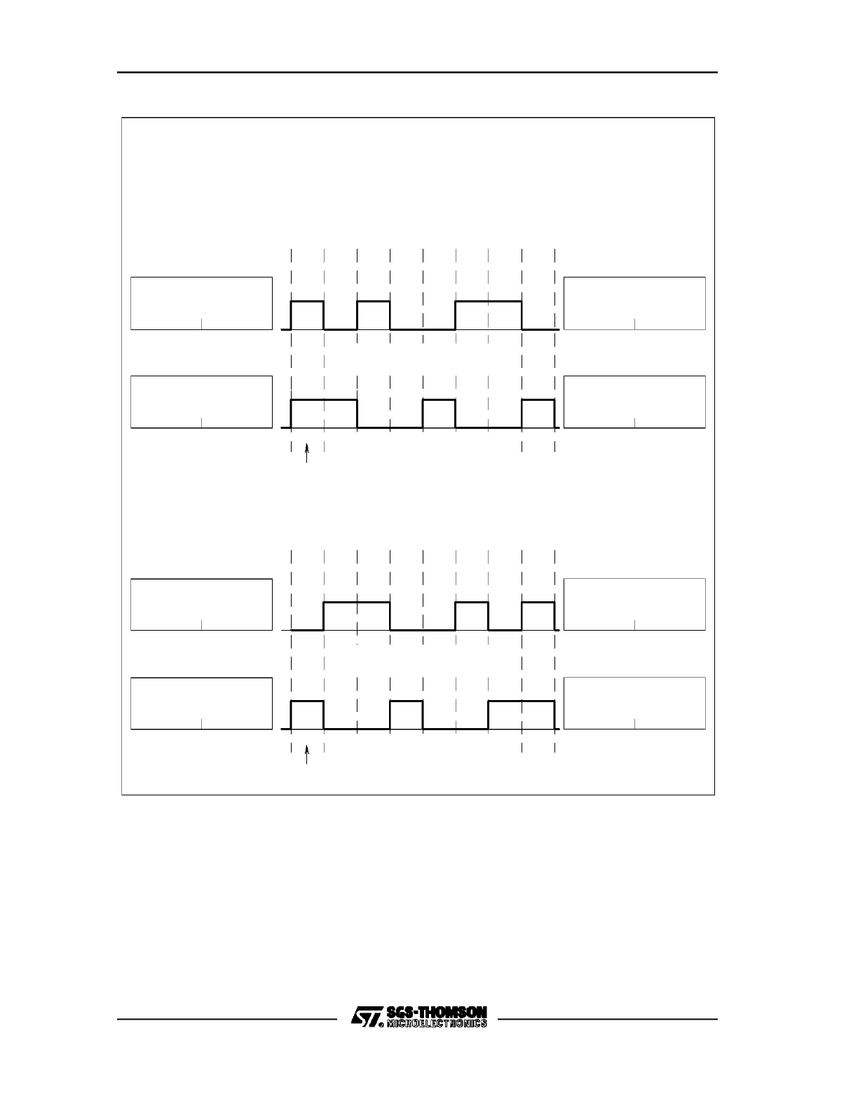
C167 FAMILY PRELIMINARY USER MANUAL
98/180
Figure 24. LSB First / MSB First Operation Examples
VR001887
Transmit Line
Register SSCTB
0000 0000
0110 0101
Register SSCTB
0110 0101
0000 0000
XXXX XXXX
XXXX XXXX
Register SSCRB
0000 0000
1001 0011
Register SSCRB
65h
00h
XXh
XXh
Receive Line
00h
93h
Bit
0
1
2
3
4
5
6
7
00h
65h
Before Transmission
Transmission/Reception
Complete
LSB
a) LSB FIRST OPERATION
Transmit Line
Receive Line
b) MSB FIRST OPERATION
0110 0101
Register SSCRB
XXXX XXXX
65h
XXh
Register SSCTB
Before Transmission
0000 0000
XXXX XXXX
XXh
00h
MSB
Bit
7
5
6
4
0000 0000
0000 0000
Register SSCRB
00h
00h
Register SSCTB
Transmission/Reception
3
2
1
0
0110 0101
1001 0011
93h
Complete
65h
Example: 8-Bit Data Width
Transmit Data: 65h 0110 0101
Receive Data:
93h 1001 0011
C167 FAMILY PRELIMINARY USER MANUAL
99/180
Clock Control
Two bits in register SSCCON are provided to control the polarity and the phase of the
serial clock SCLK. Bit SSCPO allows to select the idle level of the clock. With
SSCPO = 0, the clock line is at a low level between transfers, and with SSCPO = 1,
the clock idle state is a high level. Bit SSCPH determines the operation to be
performed at a certain clock edge. For transmission, one edge of the clock signal is
always used for shifting, while the other edge is used for latching the data. Figure 25
shows the possible combinations for the clock and illustrates the shifting and latching
edges with respect to the data. With SSCPH = 1, the first edge of the clock is used
for latching the data and with the second edge, a shift by one bit is performed. With
SSCPH = 0, the selection is performed vice versa.
With this flexible control, an adaption to a variety of different operating modes of
other synchronous serial interfaces is possible.
Figure 25. Serial Clock Phase and Polarity Options
VR001888
Data
Shift Data
Serial Clock
Pins
MTSR/MRST
SSCPO
SSCPH
SCLK
0
1
0
0
0
1
1
1
Transmit
First
Bit
Latch Data
Bit
Last
Error Detection
Four different types of error conditions can be detected by the SSC. If an error
occurs, an error interrupt request can be generated in order to allow appropriate
reactions in such a case. For each of these types of error, a separate error detection
enable bit and error indication flag is provided in register SSCCON. A detailled
discussion of the types of error detection can be found in Chapter 7.5.

C167 FAMILY PRELIMINARY USER MANUAL
100/180
Busy Flag
The busy flag, SSCBSY, accessible only when the SSC is enabled (SSCEN = 1),
indicates whether a transfer is currently in progress or not. The busy flag is set and
reset by hardware, and software should only read this bit to check the status of the
SSC. SSCBSY is set in master mode when the contents of SSCTB is copied to the
shift register, and transmission begins. It remains set until the last transfer has been
finished. That means, as long as the transmit buffer SSCTB is not empty, transfers
are continued, and SSCBSY remains set.
In the slave mode, SSCBSY is set as soon as the value in the transmit buffer is
copied into the shift register, and remains set until the last bit of the last data is
received. That means, the busy flag is not reset between continuous transfers (see
Chapter 7.4.4 for details on continuous transfers).
SSC Bit Count Field
When the SSC is disabled, the lower four bits, SSCBM, of register SSCCON are
used to initialize the data width of the transfer data. When the SSC is enabled, these
four bits represent the shift counter, SSCBC, and are updated with each shift.
Software should never modify this bit field if the SSC is enabled, and should only
read SSCBC if certain analysis routines are necessary after the occurence of an
error.
7.3.2 Buffer Registers SSCTB and SSCRB
Register SSCTB holds the data to be transmitted, while SSCRB contains the data
which was received during the last transfer. Both registers are 16-bit registers,
however, only the number of least significant bits defined through the data transfer
width in SSCBM are relevant. This means, for example, when the data transfer width
is set to 10 bits, bits 0 through 9 hold the data to be transmitted or received, while
bits 10 through 15 are unused. As mentioned above, the data in these registers is
always right aligned, that means, bit 0 of these registers always holds the LSB of the
data. A further discussion of the operation of these registers can be found in
Chapters 7.4.
7.3.3 Baud Rate Register SSCBR
This 16-bit register is used to program the serial transfer baud rate. When the SSC is
disabled, register SSCBR can be loaded with the baud rate value. Reading this
register returns either ’0000’ (default after reset) or the programmed baud rate value.
The baud rate generator is a down counter, and uses the value in SSCBR as a
reload value. The baud rate generator is started when the SSC is enabled through
setting bit SSCEN. When SSCEN is ’1’, SSCBR should never be written to. Reading
SSCBR while the SSC is enabled returns the current count of the baud rate
generator. It is recommended, however, to only access register SSCBR when the

C167 FAMILY PRELIMINARY USER MANUAL
101/180
SSC is disabled. The baud rate generator is clocked with CPU Clock /2, such that a
maximum baud rate of up to 5 MBaud is available. The formula for calculating the
baudrate is
SSC Baud Rate = CPU Clock / (2 * (SSCBR + 1)),with SSCBR > 0
or, for a desired baud rate the calculation of the reload value SSCBR is
SSCBR = (CPU Clock / (2 * Baud Rate)) - 1,SSCBR must be > 0
It must be noted that, although the clock is only generated in the master mode
operation, if one wants to use the baud rate error detection capability, the baud rate
must also be correctly programmed to the serial system baud rate in the slave mode.
The following table gives an overview of some possible baud rates at a CPU Clock of
20 MHz, together with the resulting bit times:
SSCBR
Baud Rate
Bit Time
0000h
0001h
0002h
0003h
0004h
0009h
0063h
03E7h
270Fh
FFFFh
reserved
5 MBaud
3.3 MBaud
2.5 MBaud
2.0 MBaud
1.0 MBaud
100 KBaud
10 KBaud
1.0 KBaud
152.6 Baud
200 ns
300 ns
400 ns
500 ns
1 us
10 us
100 us
1 ms
6.6 ms
7.3.4 Interrupt Control Registers
Three interrupt control registers are associated with the SSC, one for a transmit
interrupt (SSCTIC), one for a receive interrupt (SSCRIC), and one for an error
interrupt (SSCEIC). These registers and their functions, shown hereafter, are
identical to all other interrupt control registers in the C167 (and in the entire
ST10x166 family), and are not explained here (please refer to the ST10 User Manual
for details). The conditions for generating the individual interrupt requests are
explained in Chapters 7.4 and 7.5.

C167 FAMILY PRELIMINARY USER MANUAL
102/180
SSCTIC (FF72h/B9h)
Synchronous Serial Channel Transmission Interrupt Control
Reset Value: 0000h
0
1
2
3
4
5
6
7
SSCTIR
SSCTIE
GLVL
ILVL
b7 = SSCTIR: SSC Transmission Interrupt Request.
b6 = SSCTIE: SSC Transmission Interrupt Enable.
b5 to b2 = ILVL: Interrupt Priority Level.
b1, b0 = GLVL: Group Priority.
SSCRIC (FF74h/BAh)
Synchronous Serial Channel Reception Interrupt Control
Reset Value: 0000h
0
1
2
3
4
5
6
7
SSCRIR
SSCRIE
GLVL
ILVL
b7 = SSCRIR: SSC Reception Interrupt Request.
b6 = SSCRIE: SSC Reception Interrupt Enable.
b5 to b2 = ILVL: Interrupt Priority Level.
b1, b0 = GLVL: Group Priority.
SSCEIC (FF76h/BBh)
Synchronous Serial Channel Error Interrupt Control
Reset Value: 0000h
0
1
2
3
4
5
6
7
SSCEIR
SSCEIE
GLVL
ILVL
b7 = SSCEIR: SSC Error Interrupt Request.
b6 = SSCEIE: SSC Error Interrupt Enable.
b5 to b2 = ILVL: Interrupt Priority Level.
b1, b0 = GLVL: Group Priority.
C167 FAMILY PRELIMINARY USER MANUAL
103/180
7.3.5 Port Control Registers
The SSC uses three pins of port P3 to operate with the external world. Pin
P3.13/SCLK serves as the clock line, while pins P3.8/MRST (Master Receive/Slave
Transmit) and P3.9/MTSR (Master Transmit/Slave Receive) serve as the serial data
input/output lines. Figure 26 shows the configuration of the port structure for these
pins.
Figure 26. SSC Alternate Input / Output Port Structures
C167 FAMILY PRELIMINARY USER MANUAL
104/180
The operation of these pins depend on the selected master or slave mode (see
tables). In order to enable the alternate output functions of these pins instead of the
general purpose I/O operation, the respective port latches have to be set to ’1’, since
the port latch outputs and the alternate output function lines are ANDed. When the
alternate data output line is not used, it is held at a high level, allowing I/O operations
via the port latch. The direction of the port lines is depending on the master or slave
operation. The SSC will automatically use the correct alternate input or output line of
the ports when switching the modes, however, the direction of the pins must be
programmed by the user, as shown in the tables.
Master Mode
Pin
Operation
Port Latch
Direction Bit
P3.13/SCLK
P3.9/MTSR
P3.8/MRST
Serial Clock Output
Serial Data Output
Serial Data Input
P3.13 = 1
P3.9 = 1
P3.8 = x
DP3.13 = 1
DP3.9 = 1
DP3.8 = 0
Slave Mode
Pin
Operation
Port Latch
Direction Bit
P3.13/SCLK
P3.9/MTSR
P3.8/MRST
Serial Clock Input
Serial Data Input
Serial Data Output
P3.13 = x
P3.9 = x
P3.8 = 1
DP3.13 = 0
DP3.9 = 0
DP3.8 = 1
In the tables above, an ’x’ means the actual value is irrelevant, however, it is
recommended to set these bits to ’1’, such that they are already in the correct state
when switching between master/slave mode.
The tables above show the programming of the direction of the pins when using
normal push/pull operation. In the C167, however, port P3 has the feature of being
switched to an open drain output mode (see Chapter 11). This is controlled by the
respective Open Drain Control Register ODP3, and can individually be selected for
each line of port P3. For the SSC, the control bits ODP3.13, ODP3.9, and ODP3.8
are relevant. This feature can perfectly be used in a serial communication system
with the SSC. It helps to avoid bus contention problems and reduces the need for
hardwired hand-shaking or slave select lines. When using the open drain feature, it is
not always necessary to switch the direction of the port pin. The application of the
open drain feature is explained in detail in Chapter 7.4.
C167 FAMILY PRELIMINARY USER MANUAL
105/180
7.4
Detailled Operation of the SSC
Figure 27 shows a block diagram of a typical serial configuration with the SSC. Three
wires are connected between the different devices: a clock line, a transmit line, and a
receive line. The clock line is connected parallel to all devices, while the connection
of the data line(s) depends on full- or half-duplex operation. This configuration can be
used for single- or multi-master operation.
Figure 27. Basic Serial Configuration with the SSC
Device n
Device 1
Device 3
VR0G1628
Device 2
MASTER
SLAVE
SLAVE
SLAVE
Clock
Transmit
Receive
1 or 2
Lines
.
.
.
C167 FAMILY PRELIMINARY USER MANUAL
106/180
7.4.1 Single Master, Full-Duplex Operation
Such a configuration is illustrated in Figure 28. The master device can either be a
C167, or a member of the ST10 or 8051 families (LSB first operation only), or other
master mode capable devices compatible to the SSC. As slave devices, C167
components, or again devices compatible to the SSC and capable of slave mode
operation, can be used. Due to being only capable to operate in the master mode,
the ST10x166 or members of the 8051 family cannot be used as slave devices. To
simplify the further description, it is assumed that only C167 components are used
for both, master and slave devices, if not stated otherwise.
Figure 28. Full-Duplex, Single Master Configuration Example
Shift Register
Clock
MTSR
MRST
CLK
Transmit
Receive
Clock
Shift Register
Clock
CLK
MTSR
MRST
Device 2
Slave
Master
Device 1
Slave
Device 2
MRST
MTSR
CLK
Clock
Shift Register
VR001909
As mentioned before, the different devices are connected through three lines. The
definition of these lines is always determined by the master: The line connected to
the master’s data output pin MTSR is the transmit line, the receive line is connected
to it’s data input line MRST, and the clock line is the line connected to pin SCLK. Only
the device selected for master operation can generate and output the serial clock at
pin SCLK. All slaves must receive this clock, pin SCLK is an input. In the block
diagram, only the actual shift register of a device’s synchronous serial interface is
represented, with an indication of the shift direction (this is regardless whether the
MSB or LSB is shifted first). The external transmit line is connected to the input of a

C167 FAMILY PRELIMINARY USER MANUAL
107/180
slave’s shift register. The output of the slave’s shift register is connected to the
external receive line in order to enable the master to receive the data shifted out of
the slave. Since the external lines are hard-wired, also the pins connected to these
lines are fixed. Therefore it is obvious, that the function and direction of these pins is
determined by the master or slave operation of the individual device. That is the
reason, why the pins MTSR and MRST have to reverse their meaning and direction
on a slave device.
To operate with this configuration, first all devices must be initialized according to the
desired operation. One of the devices must be selected for master operation
(SSCMS = 1), all others must be programmed to slave operation (SSCMS = 0).
Besides the modes of operation of the device’s SSC, the respective port lines have to
be initialized according to the table shown for master and slave mode (clock line
exceptions see note below). However, when studying the block diagram, one can
see, that the slave’s data output pins MRST are connected together onto on line.
Without provisions, this would result in a short circuit when the slaves try to drive
different logic levels onto this line. Of course, only one slave is allowed to output it’s
transmit data onto this line, however, the other slaves would drive their idle state onto
this line. There are two ways to avoid this collision: One is that all, or all except one,
of the slaves program there MRST pins to input. That means, that no or only one
slave can put it’s data onto the master’s receive line. Only receiving of data from the
master is possible. The master has to select the slave device from which it expects
data either by separate select lines, or by sending a special command to the slave.
The selected slave then would program it’s MRST line for output, until it gets a
deselection signal or command. The other way is by using the open drain output
feature. For this, an external pullup device is connected to the serial receive line, and
all slaves program their MRST line to open drain output. This forms a Wired-AND
connection. To avoid the corruption of the data on the receive line if two or more
slaves try to place different logic levels onto this line, all slaves which are not
selected for transmission to the master just have to transmit the value ’FFFFh’
(depending on selected data width). Since in this case the high level is not actively
driven onto the line, but only held through the pullup device, the selected slave can
pull this line actively to a low level without the danger of a short circuit.
After performing all necessary initializations of the SSC, the serial interfaces can be
enabled. For a master device, the alternate clock line will now go to its programmed
polarity. The alternate data line will go to either ’0’ or ’1’, until the first transfer will
start (for further transfers, the alternate data line will always remain at the logic level
of the last transmitted data bit).

C167 FAMILY PRELIMINARY USER MANUAL
108/180
Note: The state of the internal alternate output lines is a ’1’ as long as the SSC is
disabled. If the SCLK pin of the master is already completely initialized at the time the
SSC is enabled, an unwanted clock edge could be produced when the SSC is
enabled in the case a clock polarity of ’0’ is selected. Due to the ANDing of the port
latch value and the alternate data output, the pin will switch from a ’1’ to a ’0’. To
avoid this, first the SSC of the master should be enabled, then the port latch should
be programmed to a ’1’. In the case of a clock polarity of ’1’, the port latch should be
first programmed to ’1’.
When the serial interfaces are enabled, the master device can initiate the first data
transfer. This is performed by writing the transmit data into register SSCTB. This
value is copied into the shift register (which is assumed to be empty at this time), and
with the next signal of the baud rate generator, the busy flag and the transmit
interrupt request flag will be set. The selected first bit of the transmit data will be
placed onto the MTSR line. Depending on the selected clock phase, also a clock
pulse will be generated on the SCLK line (see Figure 25). The master then continues
to shift out the contents of it’s shift register with each clock pulse, while at the same
time latching and shifting in the data detected at it’s input line MRST. Since the clock
line is connected in parallel to all slaves, their shift registers will be shifted
synchronously with the master’s shift register, shifting out the data contained in the
registers, and shifting in the data detected at the input line. After the preprogrammed
number of clock pulses (via the data width selection) have been generated, the data
transmitted by the master is contained in all slave’s shift registers, while the data of
the selected slave can be found in the master’s shift register. In the master and all
slaves, the contents of the shift register is copied into the receive buffer SSCRB, and
the receive interrupt flag SSCRIR is set.
Note: The mechanism to start a transmission by writing into the transmit buffer
register SSCTB is only active when the SSC is enabled (SSCEN = 1). If register
SSCTB is written to prior to the enabling of the SSC, no transmission will start.
Other than for a master device, in a slave device the selected first bit (MSB or LSB
of the transfer data) will immediately be put out at pin MRST when the contents of the
transmit buffer is copied into the slave’s shift register. In a master device, this will
occur with the next signal from the baud rate generator. The reason for this is that,
depending on the selected clock phase, the first clock edge generated by the master
may be already used to clock in the first data bit. Thus, the slave’s first data bit must
already be valid at this time. This behaviour can also be seen in Figure 25.
One can see that, other than for the asynchronous serial interface ASC0, always a
transmission and reception takes place, regardless whether valid data has been
transmitted or received.
C167 FAMILY PRELIMINARY USER MANUAL
109/180
7.4.2 Multi-Master, Full-Duplex Operation
Figure 29 basically shows the same configuration as Figure 28, however, now the
role of the master has been passed to the next device, either through a type of token
passing scheme, or through special hand-shaking lines. The previous master is now
switched to the slave mode by setting bit SSCMS to ’0’, and the previous slave is
now the master (SSCMS = 1). Since the external connections can not be changed,
one can see that the new master and the previous master both have switched their
connection of the shift register input and output to the respective port lines. This
switch is automatically performed when switching from master to slave mode and
vice versa. The port direction control, however, must be changed by the user, as
already explained above.
The basic operation now is the same as described for a single master system (also in
a multi-master system, at one time, only one single master can exist).
Figure 29. Full-Duplex, Multi-Master Configuration Example
Shift Register
Clock
MTSR
MRST
CLK
Transmit
Receive
Clock
Shift Register
Clock
CLK
MTSR
MRST
Device 2
Slave
Master
Device 1
Slave
Device 3
MRST
MTSR
CLK
Clock
Shift Register
VR001910
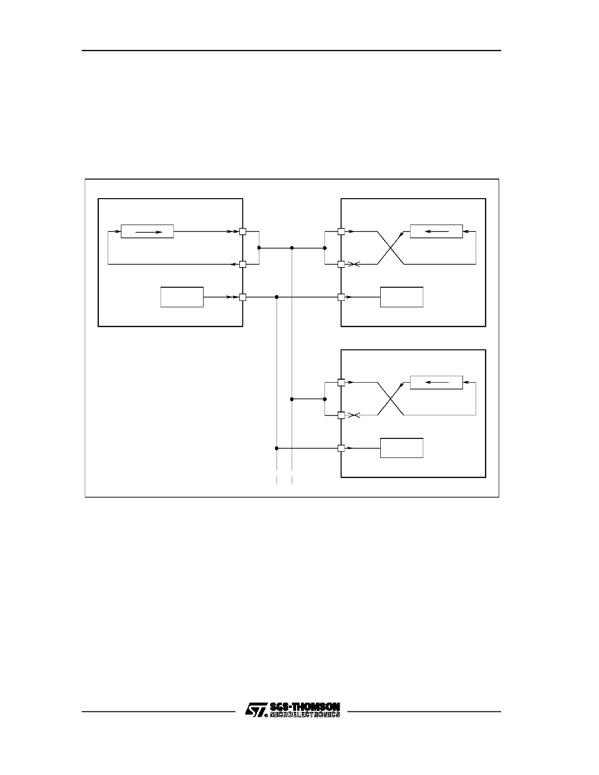
C167 FAMILY PRELIMINARY USER MANUAL
110/180
7.4.3 Half-Duplex Operation
It is also possible, to use only one data line for receive and transmit between the
devices. Figure 30 shows such a configuration. As for the full-duplex mode, the clock
line is again connected in parallel to all devices. The data input and output pins,
however, are all connected together onto one line.
Figure 30. Half-Duplex Configuration Example, Push/Pull Outputs
Shift Register
Clock
MTSR
MRST
CLK
Clock
Shift Register
Clock
CLK
MTSR
MRST
Device 2
Slave
Master
Device 1
Slave
Device 3
MRST
MTSR
CLK
Clock
Shift Register
VR0A1910
Transmit/
Receive
Common
Line
Other than for the full-duplex configuration, where a transmission from a slave to a
slave is not possible,
transmissions/receptions between any stations can be
performed with the half-duplex configuration. Depending on the output driver mode of
the port pins, different methods can be used to avoid conflicts on the serial data line.
When using push/pull output drivers, only the transmitting device may enable its data
output pin, as shown in Figure 31. All other devices must disable their output drivers
through switching the port line to input. The clock signal for the transfer is provided
by the master device. All devices, even the transmitting device, can receive the data.

C167 FAMILY PRELIMINARY USER MANUAL
111/180
Figure 31. Example: Half-Duplex Config., Slave Transmit, Push/pull Outputs
Shift Register
Clock
MTSR
MRST
CLK
Clock
Shift Register
Clock
CLK
MTSR
MRST
Device 2
Slave
Master
Device 1
Slave
Device 3
MRST
MTSR
CLK
Clock
Shift Register
VR0B1910
Transmit/
Receive
Common
Line
With the open drain output configuration, shown in Figure 32, no enabling or disabling
of the port lines is necessary for the half-duplex mode. Instead, a line conflict is
avoided through setting the data in the non-transmitting devices’ shift registers to all
ones.
Since the data inputs and outputs are connected together, a transmitting device will
clock in it’s own data at the input pin (MRST for a master device, MTSR for a slave).
In this way, it is possible to detect any corruptions on the common data line, if the
received data is not equal to the transmitted data.
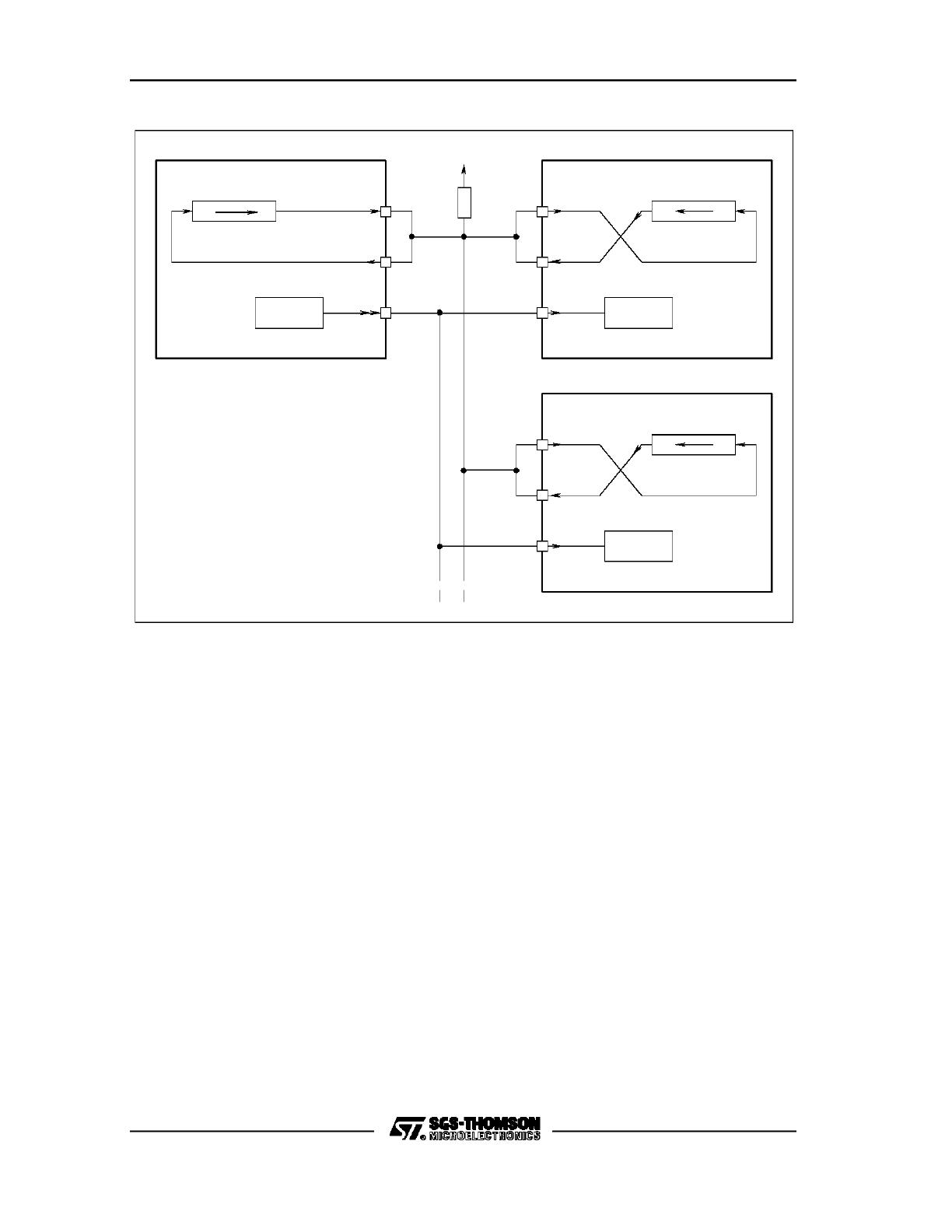
C167 FAMILY PRELIMINARY USER MANUAL
112/180
Figure 32. Example: Half-Duplex Config., Slave Transmit, Open Drain Outputs
Shift Register
Clock
MTSR
MRST
CLK
Clock
Shift Register
Clock
CLK
MTSR
MRST
Device 2
Slave
Master
Device 1
Slave
Device 3
MRST
MTSR
CLK
Clock
Shift Register
VR0C1910
Transmit/
Receive
Common
Line
FFFFh
FFFFh
ABCDh
7.4.4 Continuous Transfers
When the transmit interrupt request flag is set, it indicates that the transmit buffer
SSCTB is empty and ready to be written to with the next transmit data. If, by the time
a previous transmission is finished, register SSCTB is full, it is immediately
transferred into the shift register and the next transmission will start without any extra
delay. From an external point of view, a transmission of two data frames in this case
would look like a transmission of one data frame of double the data length. Two byte
transfers, for example, would produce the same characteristics as one word transfer.
This feature can be used to interface with devices which can operate with or require
more than 16 data bits per transfer. It is just a matter of software, how long a total
data frame length can be. Of course, this can only happen in multiples of the selected
basic data width, since it would require disabling/enabling of the SSC to reprogram
the basic data width on-the-fly. This option can also be used to, for example,
interface to byte- and word-wide slaves at the same serial bus.

C167 FAMILY PRELIMINARY USER MANUAL
113/180
7.5
Error Detection
Four different types of error conditions can be automatically detected by the SSC.
Two of these can be detected in master mode, while in slave mode all four can be
detected. An error indication flag SSCxE will be set if the error condition occurs, and
an error interrupt request can optionally be generated.
Error Type
Defined for
Enable Bit
Indication Flag
Transmit Error
Receive Error
Phase Error
Baudrate Error
Slave Mode
Master and Slave Mode
Master and Slave Mode
Slave Mode
SSCTEN
SSCREN
SSCPEN
SSCBEN
SSCTE
SSCRE
SSCPE
SSCBE
The error detection enable bits SSCxEN are only accessible for initialization when
the SSC is disabled (SSCEN = 0), while the respective error indication flags are
accessible only when the SSC is enabled (SSCEN = 1). When an error occurs, in
any case the respective error indication flag SSCxE will be set. All four error types
can be programmed to generate the same error interrupt SSCEINT, controlled
through register SSCEIC. This interrupt request, however, will only be generated
when an error condition occurs and the respective error enable bit was set during the
initialization of the SSC. Figure 33 shows a functional diagram of the error interrupt
generation. In the error interrupt service routine, the error indication flags in register
SSCCON can be polled to determine which type of error had occurred. While the
general error interrupt request flag SSCEIR is automatically cleared by hardware
when the interrupt is serviced, the error indication flags SSCxE must be cleared by
software, otherwise further interrupt requests may be generated after the return from
the service routine.
In this way, it is possible to program one or more error conditions to generate an
error interrupt, while checking the remaining error conditions through software polling
techniques.
Note that, if enabled through the respective enable bit SSCxEN, the setting of an
error indication flag SSCxE by software will also cause the error interrupt request flag
SSCEIR to be set. This can be used for testing the respective error service routine
without having to specifically produce the error condition.
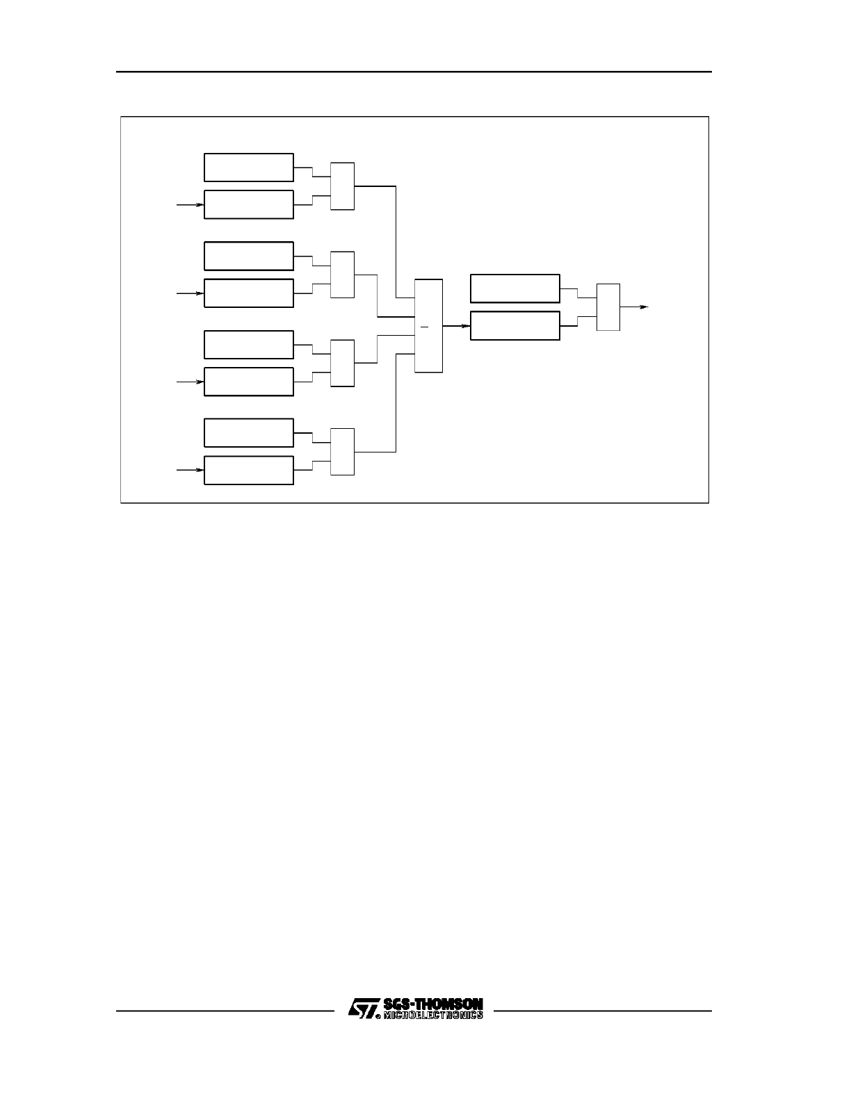
C167 FAMILY PRELIMINARY USER MANUAL
114/180
Figure 33. SSC Error Interrupt Control
VR001911
SSCTEN
Register SSCCON
Register SSCEIR
SSCTE
> 1
&
Transmit
Error
Error
Receive
&
SSCRE
SSCREN
Error
Phase
&
SSCPE
SSCPEN
SSCBEN
SSCBE
&
Error
Baudrate
&
SSCEIR
SSCEIE
Error
Interrupt
SSCEINT
7.5.1 Receive Error (Master and Slave Mode)
A receive error will be generated when a new data frame is completely received, but
the previous data was not read out of the receive buffer register SSCRB. This
condition sets the indication flag SSCRE and the error interrupt request flag SSCEIR.
The old data in the receive buffer SSCRB will be overwritten with the new value and
is unretrievably lost.
7.5.2 Phase Error (Master and Slave Mode)
The incoming data at pin MRST is sampled with the same frequency as the CPU
Clock. If the data changes between one sample before and one sample after the
latching edge of the clock signal (see Figure 25), the phase error indication flag
SSCPE and the error interrupt request flag SSCEIR is set.

C167 FAMILY PRELIMINARY USER MANUAL
115/180
7.5.3 Baud Rate Error (Slave Mode)
Using this error detection capability requires that the slave’s baud rate generator is
programmed to the same baud rate as the master device. The baud rate error
indication flag will then be set if the incoming clock signal deviates from the
programmed baud rate such, that it either is more than double or less than half the
expected baud rate. This feature allows to detect false additional, or missing pulses
on the clock line (within a certain frame). The indication flag SSCBE and the error
interrupt request flag SSCEIR will be set on such a condition.
If this error condition is enabled to generate an interrupt request through setting bit
SSCBEN during the initialization of the SSC, an automatic reset of the SSC will occur
in the case of this error. This is done to reinitialize the SSC, if too less or too many
clock pulses have been detected.
7.5.4 Transmit Error (Slave Mode)
This error indicates that a transfer was initiated by the master, but the transmit buffer
SSCTB of the slave was not updated, i.e. not written to with a new value. If a transfer
starts while the transmit buffer is not updated, the slave will shift out the ’old’ contents
of the shift register, which normally is the data received during the last transmission.
In the half-duplex, open drain serial configuration, such an operation will lead to a
corruption of the data on the transmit/receive line, if this slave is not selected for
transmission. This mode requires that slaves not selected for transmission shift out
all ones, thus, their transmit buffers must be loaded with the value ’FFFFh’
(depending on selected transfer data width) prior to any transfer.
When using push/pull output drivers, the value shifted out of the shift register of a
slave not selected for transmission will normally present no problem, since the output
is switched off in this case. However, in order to avoid possible conflicts or
misinterpretations, it is recommended to always load the slave’s transmit buffer prior
to any transfer.

C167 FAMILY PRELIMINARY USER MANUAL
116/180

C167 FAMILY PRELIMINARY USER MANUAL
117/180
8.
A/D CONVERTER (ADC)
The ADC-Module is based on the module implemented in the ST10x166, enhanced
by additional analog input channels, two new operating modes, a second result
register, ADDAT2, and a programmablity for the sample and conversion times. In the
following, the new additional functions and features are described.
8.1
Additional A/D Input Channels
The C167 has 16 analog input channels to the on-chip A/D Converter. For this
purpose, the input-only Port 5 is extended to 16 bits. The channel selection field
ADCH in the A/D Converter Control register ADCON now allows the specification of
all sixteen channels. The following table lists all Port 5 pins and their alternate
functions together with the selection via ADCH:
Pin
Alternate Function
Channel
Selection ADCH
P5.0
AN0
Analog Input 0
0000
P5.1
AN1
Analog Input 1
0001
P5.2
AN2
Analog Input 2
0010
P5.3
AN3
Analog Input 3
0011
P5.4
AN4
Analog Input 4
0100
P5.5
AN5
Analog Input 5
0101
P5.6
AN6
Analog Input 6
0110
P5.7
AN7
Analog Input 7
0111
P5.8
AN8
Analog Input 8
1000
P5.9
AN9
Analog Input 9
1001
P5.10
AN10
Analog Input 10
1010
P5.11
AN11
Analog Input 11
1011
P5.12
AN12
Analog Input 12
1100
P5.13
AN13
Analog Input 13
1101
P5.14
AN14
Analog Input 14
1110
P5.15
AN15
Analog Input 15
1111
The lines of Port 5 can also be used as digital inputs. No special distinction has to be
made between Port 5 lines being used as analog inputs and Port 5 lines being used
as digital inputs. For more information on Port 5 please refer to the ST10 User
Manual.
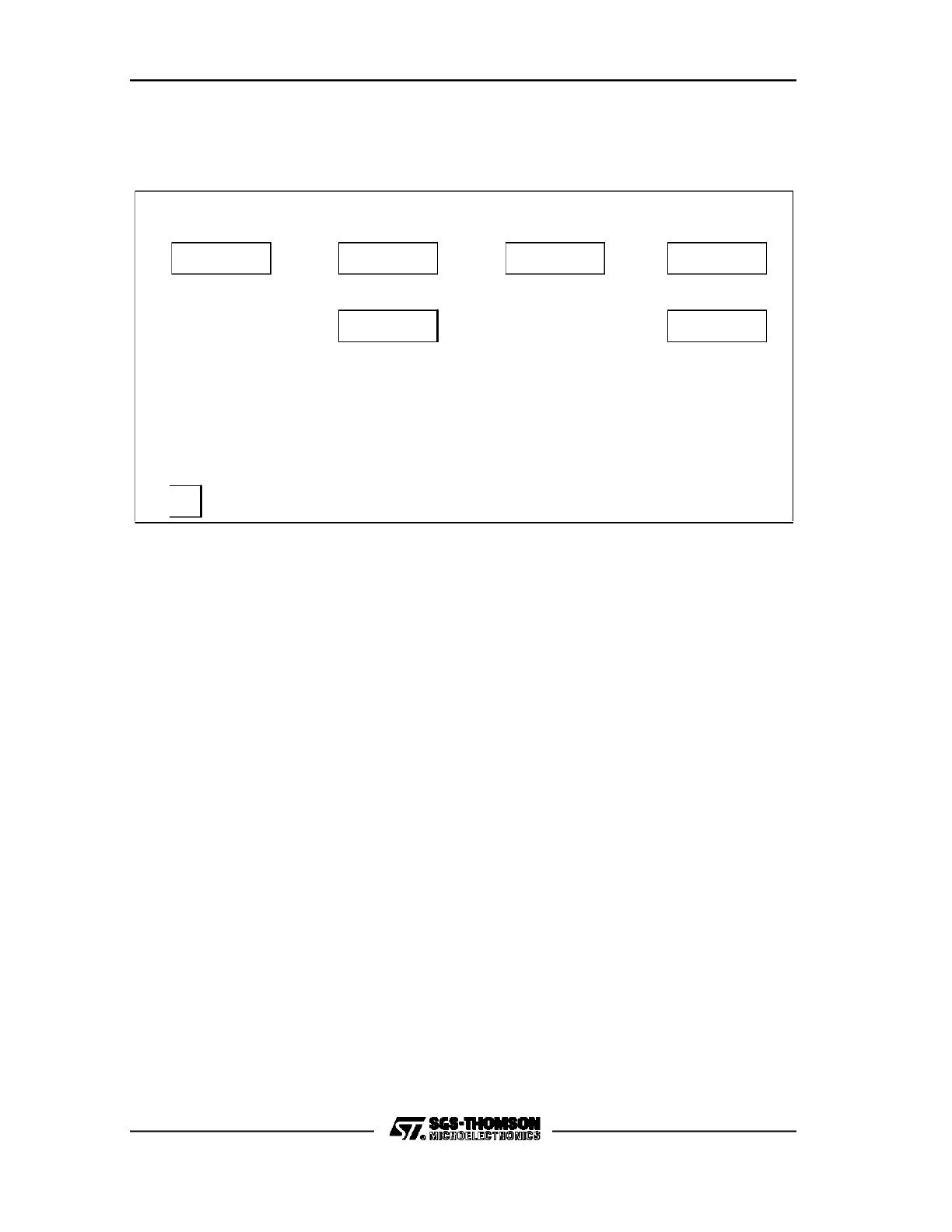
C167 FAMILY PRELIMINARY USER MANUAL
118/180
Note that in the C167, the upper six lines of Port 5 have a second alternate function
for the GPT1 and GPT2 timer inputs.
Figure 34. SFRs and Port Pins Associated with the A/D Converter
VR0A1914
Ports
Data
Control
* Registers in Extended SFR Space
Interrupt
AN15...AN0
P5
ADDAT
ADDAT2
Control
Registers
Registers
ADCIC
ADCON
P5.15...P5.0
ADEIC
P5
* ADDAT2
ADDAT
ADCON
ADCIC
ADEIC
Port 5 Register
A/D Converter Result Register
* A/D Converter Channel Injection Result Register
A/D Converter Control Register
A/D Converter End of Conversion Interrupt Control Register
A/D Converter Overru n Error / Channel Injection Interrupt Control Register
8.2
Wait for ADDAT Read Mode
In the default mode of the ADC, an overrun error interrupt request will be generated if
a new conversion result is written into the result register ADDAT before the last result
stored in this register was read by the CPU (or PEC). In this case, the old result will
be overwritten and is unretrievably lost. Note that in the continuous and auto scan
modes, the ADC immediately starts a new conversion when the current conversion is
completed.
In order to avoid the overrun error, a relatively high interrupt priority level must be
assigned to the conversion complete interrupt, and short interrupt response times
must be guaranteed due to the fast conversion time of the ADC. In many
applications, especially when operating with external program memory requiring a
number of wait states, it may be hard to fulfill this requirement.
In the C167, a new operational mode is implemented which helps to overcome such
problems. In this mode, selected by bit ADWR (Wait for Read Control Bit, ADCON.9,
see hereafter), a double-buffering of the ADDAT result register is performed. At the
completion of a conversion the ADC writes the result into register ADDAT, and starts
the next conversion. When this conversion is complete, the ADC checks whether the
previous result was read out of register ADDAT. If this is true, the new result is
written to ADDAT, and the next conversion is started. However, if the previous result
was not read in the meantime, the ADC stores the new result in a temporary latch
and waits in an idle loop. It will not start the next conversion. When finally register
C167 FAMILY PRELIMINARY USER MANUAL
119/180
ADDAT is read either by the CPU or the PEC, the new result is transferred from the
temporary latch to ADDAT, an interrupt request is generated, and the converter
starts the next conversion. This procedure is also true if the previous conversion was
a single channel conversion or the last conversion of a series of conversions (e.g.
continuous or auto scan), and the converter is started again by software. No overrun
error interrupt request will be generated in this mode, since this condition is not
possible.
ADCON (FFA0h/D0h)
A/D Converter Control Register
Reset Value: 0000h
R
ADCRQ
ADCIN
ADWR
ADBSY
15
14
13
12
11
10
9
8
0
1
2
3
4
5
6
7
R
R
R
ADST
R
ADM
ADCH
b15 to b12 = R: Reserved.
b11 = ADCRQ: ADC Channel Injection Request Flag.
Can be set by software or by a capture / compare event of register CC31 to trigger
a channel injection. This bit has only an effect if ADCIN = 1.
ADCRQ = 0: No channel injection request.
ADCRQ = 1: Channel injection request enabled.
b10 = ADCIN: ADC Channel Injection Enable control bit.
ADCIN = 0: Channel injection disabled.
ADCIN = 1: Channel injection enabled.
b9 = ADWR: ADC Wait for Read control bit.
ADWR = 0: New conversion is immediately started in autoscan or continuous
modes ; overrun error enabled.
ADWR = 1: New conversion in autoscan or continuous modes is not started if
ADDAT / ADDAT2 is full and new conversion results is ready ; overrun error is
disabled.
b8 = ADBSY: ADC Busy Flag.
ADBSY = 0: No conversions in progress.
ADBSY = 1: Conversion in progress.
b7 = ADST: ADC Start bit.
b6 = R: Reserved.
b5, b4 = ADM: ADC Mode Selection.
b3 to b0 = ADCH: ADC Analog Input Channel Selection.

C167 FAMILY PRELIMINARY USER MANUAL
120/180
An internal flag, ADDAT Full (the same used for flagging an overrun error), is used to
indicate a write of a conversion result to register ADDAT. As long as this flag is set in
the Wait for Read mode and a new conversion result is present (in the temporary
latch), the start of new conversions is disabled. When register ADDAT is read by the
CPU or a PEC transfer, the internal flag is reset and the next conversion will start.
The ADC Busy Flag, ADBSY, and the Start Flag, ADST, remain set while the
converter is waiting for a read of ADDAT.
In the default operating mode with overrun error generation, continuous or auto scan
conversions are started in a fixed timeframe (the specified conversion time). In the
wait for read mode, the time required for several conversions is dependent on the
response time of the routine reading the result register ADDAT. Thus, the time for
several conversions in the new mode can not under all circumstances be
predetermined. However, as long as software is able to keep track with the A/D
converter, there are no delays, and the ADC runs with the fastest possible speed.
Figure 35 illustrates the differences between the default mode and the new Wait for
Read mode of the ADC.
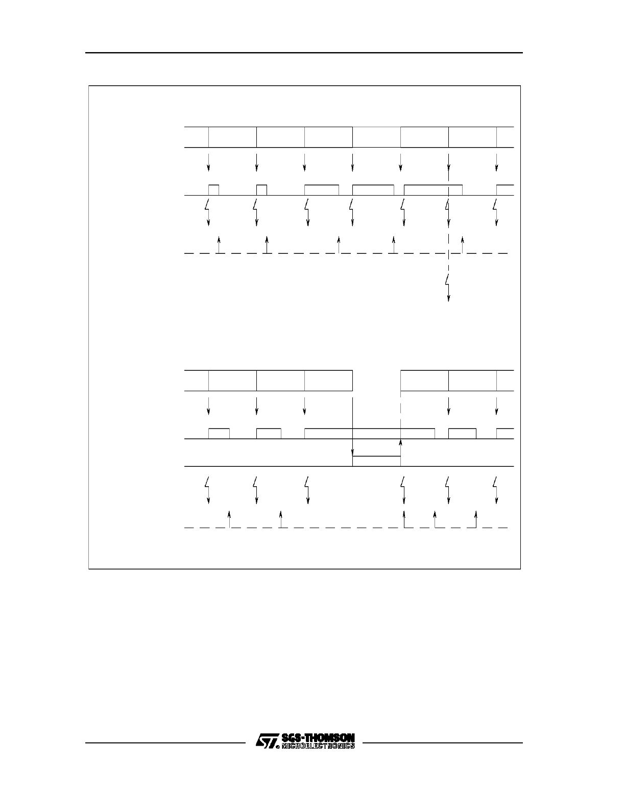
C167 FAMILY PRELIMINARY USER MANUAL
121/180
Figure 35. A/D Converter Wait for Read Mode Example
3
2
1
0
3
2
Conversion
of Channel...
X
3
2
1
3
0
Example: Auto Scan Continuous Mode; Default Operation (ADWR = 0)
Write ADDAT
ADDAT Full
Generate
Interrupt Request
Read of ADDAT;
Result of Channel:
3
1
3
X
2
Channel 0
ADDAT Full
Result Lost
Overrun Error
Interrupt Request
Hold Result in
Temp-Latch
2
X
3
Result of Channel:
Read of ADDAT;
Interrupt Request
Generate
ADDAT Full
Write ADDAT
0
3
1
2
3
X
of Channel...
Conversion
3
0
1
2
3
Auto Scan Continuous Mode with Wait for Read Operation (ADWR = 1)
..wait..
Temp-Latch
Full
1
1
0
VR001912

C167 FAMILY PRELIMINARY USER MANUAL
122/180
8.3
Channel Injection Mode
In many applications, it is necessary to convert a specific analog channel in response
to a time event or another signal, while the ADC is running in a continuous or auto
scan mode. After the conversion of this specific channel, the original operating mode
of the ADC should continue.
For this purpose, a Channel Injection mode is implemented in the ADC module. This
mode allows to interrupt the current conversion mode, to inject the conversion of a
specific channel, and to then continue the interrupted operating mode where it was
left off.
The Channel Injection mode is selected with bit ADCIN (Channel Injection Enable bit,
ADCON.10) and with bit ADWR = 1 (Wait for Read mode). The channel to be
converted in this mode is specified through the upper 4 bits of a second result
register, ADDAT2. The event to trigger the channel injection can either be a compare
or a capture event of the Capture/Compare register CC31 of the CAPCOM2 Unit, or
a setting of bit ADCRQ by software. When such an event occurs, the Channel
Injection Request bit ADCRQ (ADCON.11) is set. The converter will complete the
current conversion (if any is in progress), and will then inject the conversion of the
specified channel. When the conversion of this channel is complete, the result will be
placed into the new result register, ADDAT2, and a Channel Injection Complete
Interrupt request will be generated. For this interrupt request, the ADC Overrun Error
interrupt node is used (which in the Wait for Read mode, as described above, is not
used). The new result register, ADDAT2, is organized as register ADDAT. However,
the difference is that with register ADDAT, the number of the channel just converted
is written to the upper 4 bits, while with ADDAT2, the upper 4 bits are written to by
software to specify the number of the channel to be converted by the Channel
Injection. These 4 bits in ADDAT2 are not modified by the A/D converter.
Note: Since there is no buffering of the channel number for an injected conversion,
the upper four bits of ADDAT2 must never be modified during the sample phase of
an injected conversion, otherwise the input multiplexer will switch to the new channel.
It is recommended to only change the channel number after an injected conversion
was performed and before a new one is requested.
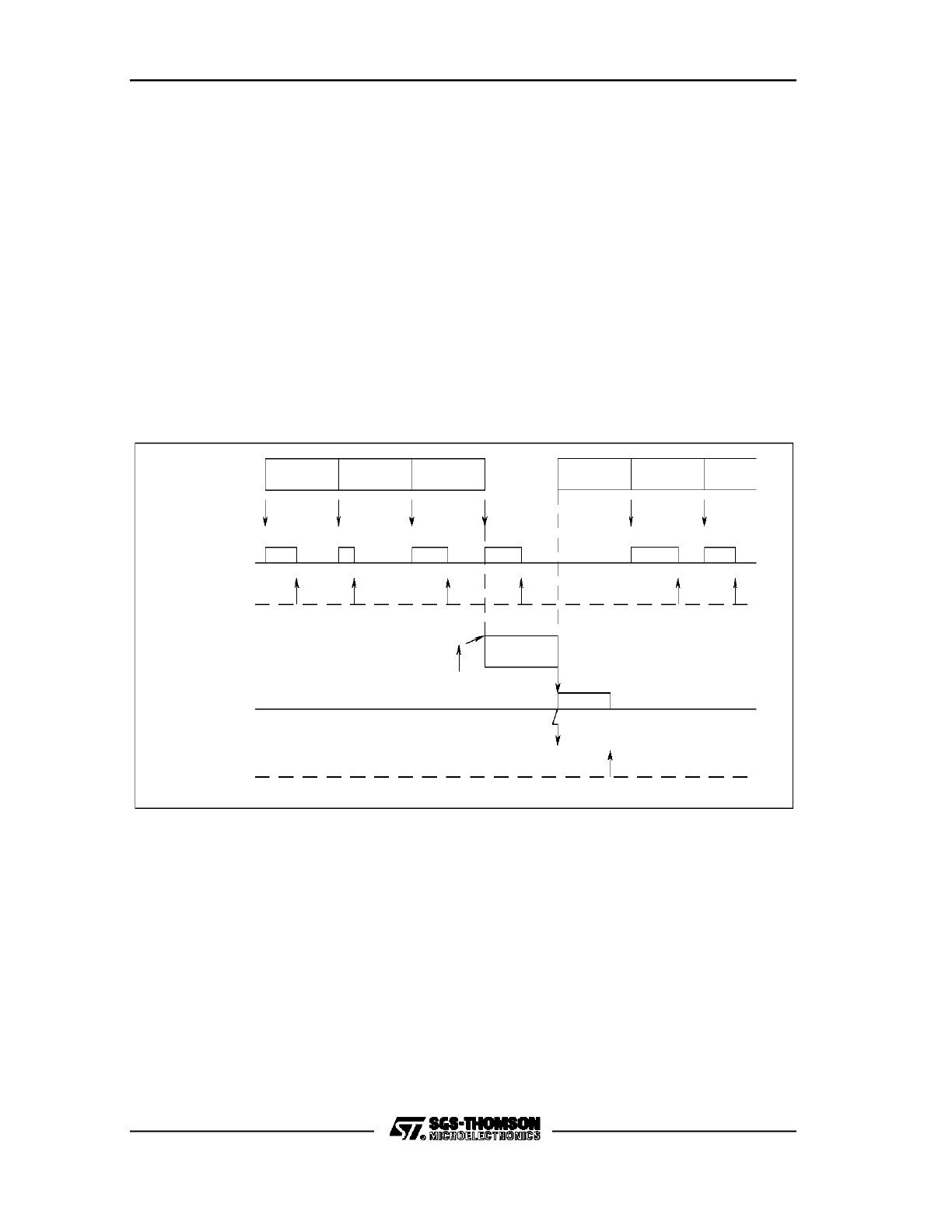
C167 FAMILY PRELIMINARY USER MANUAL
123/180
As mentioned above, the channel injection can be initiated by different events. One is
a setting of bit ADCRQ by software. The second is a compare event of
capture/compare channel CC31. This method allows to trigger a channel injection at
a specific time or on the occurence of a predefined count value of the CAPCOM
timers. The third option is a capture event of register CC31. This can be either the
positive, negative, or both the positive and the negative edge of an external signal. In
addition, this option allows to record the time of occurrence of this signal. Optionally,
the capture or compare event can generate an interrupt request (see also Chapter 5,
CAPCOM2 Unit).
Note: The channel injection request bit ADCRQ will be set through any interrupt
request of CAPCOM2 channel CC31, regardless whether the channel injection mode
is enabled or not. It is recommended to always clear bit ADCRQ before enabling the
channel injection mode.
Figure 36. A/D Converter Channel Injection Example
X
X-1
X-3
X-4
Conversion
of Channel...
X+1
X
X-1
X-3
Write ADDAT
ADDAT Full
Read ADDAT
Channel Injection
Write ADDAT2
Request by CC31
VR0A1913
X-4
X+1
X
X-1
X-3
X-4
Y
Injected
Conversion
of Channel Y
ADDAT2 Full
Read ADDAT2
Int.Request
ADEINT
X-2
X-2
X-2
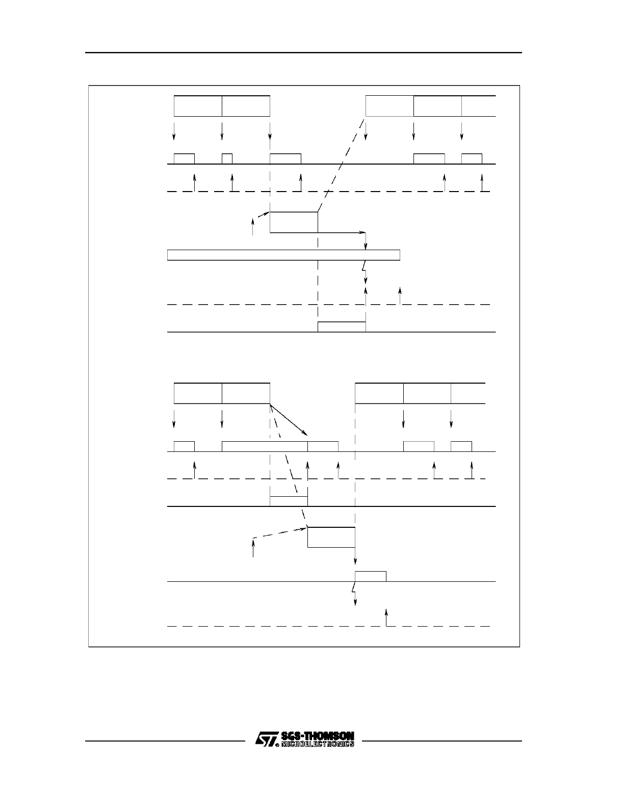
C167 FAMILY PRELIMINARY USER MANUAL
124/180
Figure 37. A/D Converter Channel Injection Wait for Read Examples
X
X-1
X-2
X-3
Conversion
of Channel...
X+1
X
X-1
X-2
0
Write ADDAT
ADDAT Full
Read ADDAT
Channel Injection
Write ADDAT2
Request by CC31
VR001913
X-3
X+1
X
X-1
X-2
X-3
Y
Y
Injected
Conversion
of Channel Y
ADDAT2 Full
Z
Read ADDAT2
Int.Request
ADEINT
Z
Y
Temp-Latch
Full
Wait until
ADDAT2 is
read
Y
ADEINT
Int.Request
Read ADDAT2
ADDAT2 Full
Y
X-3
X-2
X+1
X-3
Request by CC31
Write ADDAT2
Channel Injection
Read ADDAT
ADDAT Full
Write ADDAT
X-2
X-1
X
X+1
of Channel...
Conversion
X-3
X-2
X-1
X
X-1
X
X
Temp-Latch
Full
read
ADDAT2 is
Wait until

C167 FAMILY PRELIMINARY USER MANUAL
125/180
Figure 36 shows the operation of the channel injection mode. In Figure 37, some
special conditions are illustrated which have to be regarded when using the Channel
Injection mode. These items are described in the following:
a) When starting a channel injection, the following conditions can occur:
ADDAT
ADDAT2
TEMP_LATCH
Converter Operation
Empty
Empty
Empty
Channel Injection was started while converter was idle;
==> start conversion of injected channel
Full
Empty
Empty
Previous conversion result was written to ADDAT;
==> start conversion of injected channel
Full
Empty
Full
ADDAT Wait for Read conflict;
==> wait until ADDAT read
Full
Full
Empty
Previous conversion result was written to ADDAT;
Last Channel Injection result not read;
==> start conversion of injected channel
Empty
Full
Empty
Channel Injection was started while converter was idle;
Last Channel Injection result not read;
==> start conversion of injected channel
Full
Full
Full
ADDAT Wait for Read conflict; previous injection result not read;
==> wait until ADDAT read
Empty
Full
Full
ADDAT2 Wait for Read conflict;
==> wait until ADDAT2 read
b) At the end of an injected conversion, the following conditions can occur:
ADDAT
ADDAT2
TEMP_LATCH
Converter Operation
Empty
Full
Empty
Injected conversion result was written to ADDAT2;
==> start next conversion (if necessary, see Note)
Empty
Full
Full
ADDAT2 Wait for Read conflict; previous injection result not
read; ==> wait until ADDAT2 read
Full
Full
Empty
Injected conversion result was written to ADDAT2;
==> start next conversion (if necessary, see Note)
Full
Full
Full
ADDAT2 Wait for Read conflict; previous injection result not
read; ==> wait until ADDAT2 read
Note: The continuation of conversions is necessary in any case, if the channel
injection had interrupted either a continuous or an autoscan continuous conversion. If
an auto scan conversion was interrupted, a continuation will only be performed if the
last conversion before the channel injection was not the conversion of channel 0.

C167 FAMILY PRELIMINARY USER MANUAL
126/180
c) While an injected conversion is in progress, no further channel injection request
can be triggered. The Channel Injection Request flag ADCRQ remains set until the
the result of the injected conversion is written to the ADDAT2 register.
d) If the converter was idle before the channel injection, and during the injected
conversion the converter is started by software for normal conversions, the
channel injection is aborted, and the converter starts in the selected mode. It is
recommended therefore, to always check the busy bit ADBSY before starting a
new operation.

C167 FAMILY PRELIMINARY USER MANUAL
127/180
9.
GPT1 AND GPT2 ENHANCEMENTS
To improve the flexibility and programmability of the general purpose timers, a
number of additional input lines and control bits are provided in the C167. With this
enhancement, all of the five timers in the GPT1 and GPT2 blocks can run either in
timer and counter mode, and have the option to be controlled for up/down counting
through an external signal.
For the GPT1 timers, two additional input lines now allow the two auxiliary timers T2
and T4 to be also externally controlled for up or down counting, as it was already
implemented for the core timer T3.
For the two timers, T5 and T6, in the GPT2 block, also the option to externally control
them for up or down counting is provided through two additional input lines. For
counting external events, two more inputs have been added, thus that both, T5 and
T6, can now be used as counters.
In total, six additional input signals are implemented:
Input
Function
T2EUD
T4EUD
T5IN
T6IN
T5EUD
T6EUD
GPT1 Timer 2 External Up/Down Control Input
GPT1 Timer 4 External Up/Down Control Input
GPT2 Timer 5 External Count Input
GPT2 Timer 6 External Count Input
GPT2 Timer 5 External Up/Down Control Input
GPT2 Timer 6 External Up/Down Control Input
To control these new functions, the following additional control bits are implemented
in the respective timer control registers:
Symbol
Position
Function
T2UDE
T4UDE
T5M.1
T6M.1
T6M.0
T5UDE
T6UDE
T2CON.8
T4CON.8
T5CON.4
T6CON.4
T6CON.3
T5CON.8
T6CON.8
Timer 2 External Up/Down Control Enable Bit
Timer 4 External Up/Down Control Enable Bit
Timer 5 Mode Control Bit 1
Timer 6 Mode Control Bit 1
Timer 6 Mode Control Bit 0
Timer 5 External Up/Down Control Enable Bit
Timer 6 External Up/Down Control Enable Bit
C167 FAMILY PRELIMINARY USER MANUAL
128/180
Since a software up/down control bit, TxUD, is already implemented for all timers T2
through T6, with the additional input lines a number of options now is available for the
up/down control of the general purpose timers (x = 2..6):
Input
TxEUD
Bit
TxUDE
Bit
TxUD
Count
Direction
X
X
0
1
0
1
0
0
1
1
1
1
0
1
0
0
1
1
Up
Down
Up
Down
Down
Up
With the new mode control bits for T5 and T6, now all the options for timer, counter,
and gated timer modes are available. The following table shows these options:
T5M
T6M
Function
0 0
0 1
1 0
1 1
Timer 5/6 Timer Mode
Timer 5/6 Counter Mode
Timer 5/6 Gated Timer Mode (gate is active low)
Timer 5/6 Gated Timer Mode (gate is active high)
The bits and functions of the control registers TxCON of timers T2, T4, T5, and T6
are shown hereafter :
T2CON (FF40h/A0h)
Auxiliary Timer T2 Control Register
Reset Value: 0000h
R
R
R
R
T2UDE
15
14
13
12
11
10
9
8
0
1
2
3
4
5
6
7
T2M
R
R
T2UD
T2I
R
T2R
b15 to b9 = R: Reserved.
b8 = T2UDE: Timer 2 External Up / Down Control Enable bit.
b7 = T2UD: Timer 2Up / Down Control bit.
b6 = T2R: Timer 2 Run bit.
C167 FAMILY PRELIMINARY USER MANUAL
129/180
T2R = 0: Timer / Counter 2 stops.
T2R = 1: Timer / Counter 2 runs.
b5 to b3 = T2M: Timer 2 Mode Control.
b2 to b0 = T2I: Timer 2 Input Selection.
T4CON (FF44h/A2h)
Auxiliary Timer T4 Control Register
Reset Value: 0000h
R
R
R
R
T4UDE
15
14
13
12
11
10
9
8
0
1
2
3
4
5
6
7
T4M
R
R
T4UD
T4I
R
T4R
b15 to b9 = R: Reserved.
b8 = T4UDE: Timer 4 External Up / Down Control Enable bit.
b7 = T4UD: Timer 4 Up / Down Control bit.
b6 = T4R: Timer 4 Run bit.
T4R = 0: Timer / Counter 4 stops.
T4R = 1: Timer / Counter 4 runs.
b5 to b3 = T4M: Timer 4 Mode Control.
b2 to b0 = T4I: Timer 4 Input Selection.
T5CON (FF46h/A3h)
Auxiliary Timer T5 Control Register
Reset Value: 0000h
R
R
R
T5UDE
15
14
13
12
11
10
9
8
0
1
2
3
4
5
6
7
T5CLR
T5UD
T5I
T5SC
T5R
CI
R
T5M
b15 = T5SC: Timer 5 Capture Mode Enable bit.
T5SC = 0: Capture into register CAPREL disabled.
T5SC = 1: Capture into register CAPREL enabled.
b14 = T5CLR: Timer 5 Clear bit.
T5CLR = 0: Timer 5 is not cleared on a capture.
T5CLR = 1: Timer 5 is cleared on a capture.
b13, b12 = CI: Register CAPREL Input Selection.
b11 to b9 = R: Reserved.
b8 = T5UDE: Timer 5 External Up / Down Control Enable bit.

C167 FAMILY PRELIMINARY USER MANUAL
130/180
b7 = T5UD: Timer 5 Up / Down Control bit.
b6 = T5R: Timer 5 Run bit.
T5R = 0: Timer / Counter 5 stops.
T5R = 1: Timer / Counter 5 runs.
b5 = R: Reserved.
b4, b3 = T5M: Timer 5 Mode Control.
b2 to b0 = T5I: Timer 5 Input Selection.
T6CON (FF48h/A4h)
Auxiliary Timer T6 Control Register
Reset Value: 0000h
R
T6OTL
T6OE
T6UDE
15
14
13
12
11
10
9
8
0
1
2
3
4
5
6
7
R
T6UD
T6I
T6SR
T6R
R
R
R
T6M
b15 = T6SR: Timer 6 Reload Mode Enable bit.
T6SR = 0: Reload from register CAPREL disabled.
T6SR = 1: Reload from register CAPREL enabled.
b14 to b11 = R: Reserved.
b10 = T60TL: Timer 6 Output Toggle Latch.
Toggles on each overflow / underflow of T6.
Can be set or reset by software.
b9 = T60E: Timer 6 Alternate Output Function Enable.
T60E = 0: Alternate output function disabled.
T60E = 1: Alternate output function enabled.
b8 = T6UDE: Timer 6 External Up / Down Control Enable bit.
b7 = T6UD: Timer 6 Up / Down Control bit.
b6 = T6R: Timer 6 Run bit.
T6R = 0: Timer / Counter 6 stops.
T6R = 1: Timer / Counter 6 runs.
b5 = R: Reserved.
b4, b3 = T6M: Timer 6 Mode Control.
b2 to b0 = T6I: Timer 6 Input Selection.

C167 FAMILY PRELIMINARY USER MANUAL
131/180
External Connection of Alternate Inputs
The additional external input lines, described above, are connected to the upper six
pins of Port 5 in the C167. Since P5 is an input only port, no special programming is
necessary in order to select the alternate timer inputs. Note that Port 5 is also used
for the analog input signals for the A/D Converter. The following table shows the
reference between the upper six Port 5 pins and their alternate funtions:
Pin
Alternate
Function I
Alternate
Function II
P5.15
P5.14
P5.13
P5.12
P5.11
P5.10
AN15
AN14
AN13
AN12
AN11
AN10
T2EUD
T4EUD
T5IN
T6IN
T5EUD
T6EUD

C167 FAMILY PRELIMINARY USER MANUAL
132/180

C167 FAMILY PRELIMINARY USER MANUAL
133/180
10.
INTERRUPT SYSTEM
In the C167, a total of 56 interrupt sources and vectors is implemented. This is 24
interrupts more than in the ST10x166.
10.1 External Interrupts
As in the ST10x166, the C167 will have no dedicated external interrupt inputs.
Instead, each peripheral’s external input, which can generate an interrupt request
(such as the capture inputs of the CAPCOM units), can be used as an external
interrupt input. The sample time of the external input, however, is always tied to the
cycle time of the associated peripheral device. That means, for instance, that the
capture inputs of the CAPCOM units are sampled every 400 ns (@ 20 MHz CPU
clock), thus, external interrupt signals can only be detected in that time frame.
In order to provide faster interrupt detection, the C167 will provide the option to use 8
pins of Port 2 for fast external interrupts. If this feature is enabled, the pins P2.8
through P2.15 function as external interrupt inputs with a sample rate of 50 ns (@ 20
MHz CPU clock). This option is selected via register EXICON, External Interrupt
Control register, shown hereafter. For each interrupt input, two control bits are used
to enable the interrupt input and to select whether an interrupt is requested on the
positive, the negative, or both the positive and the negative edge of the external
signal. These interrupts use the interrupt nodes from the capture/compare registers
CC8 through CC15 of the CAPCOM1 unit, and are controlled by registers CC8IC
through CC15IC. Note that the capture and compare functions of the eight Port 2
pins can not be used when the fast external interrupts are selected (EXIxES <> ’00’),
however, the pin can be used for general purpose I/O in any case. The following
table shows the possible options for the external interrupt inputs (x = 0..7, y = x + 8):
EXIxES Selected Function
0 0
0 1
1 0
1 1
Fast Ext. Interrupt disabled; Pin can be used for capture/compare functions
Interrupt on positive edge at pin P2.y
Interrupt on negative edge at pin P2.y
Interrupt on positive and negative edge at pin P2.y
Note that the sampling of the external fast interrupt inputs is done every 50 ns (@ 20
MHz CPU Clock), the interrupt request arbitration and processing, however, is done
in steps of 200 ns.

C167 FAMILY PRELIMINARY USER MANUAL
134/180
EXICON (F1C0h/E0h)
External Interrupt Control Register
Reset Value: 0000h
15
14
13
12
11
10
9
8
0
1
2
3
4
5
6
7
EXI0ES
EXI7ES
EXI6ES
EXI5ES
EXI4ES
EXI3ES
EXI2ES
EXI1ES
b15, b14 = EXI7ES: External Interrupt 7 Edge Selection bit field.
b13, b12 = EXI6ES: External Interrupt 6 Edge Selection bit field.
b11, b10 = EXI5ES: External Interrupt 5 Edge Selection bit field.
b9, b8 = EXI4ES: External Interrupt 4 Edge Selection bit field.
b7, b6 = EXI3ES: External Interrupt 3 Edge Selection bit field
b5, b4 = EXI2ES: External Interrupt 2 Edge Selection bit field.
b3, b2 = EXI1ES: External Interrupt 1 Edge Selection bit field.
b1, b0 = EXI0ES: External Interrupt 0 Edge Selection bit field.
EXI0ES = (0,0): Fast interrupt disabled.
EXI0ES = (0,1): Interrupt on the positive edge.
EXI0ES = (1,0): Interrupt on the negative edge.
EXI0ES = (1,1): Interrupt on the positive and the negative edge.
10.2 Additional Peripheral Interrupts
In the following, the additional peripheral interrupt sources of the C167 compared to
the ST10x166 are listed. Four interrupt nodes will be implemented which have no
associated peripheral source. These interrupts can be activated through software by
setting the respective interrupt request flag XPxIR in register XPxIC. This can be
used to have software traps with programmable priority levels.
Note that the SCC interrupts will use interrupt vector locations B4h, B8h and BCh. In
the ST10x166, these interrupt vectors were used by the serial interface ASC1
interrupts (S1TINT, S1RINT, S1EINT).
Note also, that due to the replacement of the three ST10x166 ASC1 interrupts the
following table shows 27 interrupt sources. Nevertheless, the C167 has 24 interrupt
sources more than the ST10x166.
C167 FAMILY PRELIMINARY USER MANUAL
135/180
Interrupt Source
Control
Register
Interrupt
Vector
Vector
Location
Trap
Number
SCC Transmit
SSCTIC
SCTINT
B4h
2Dh
SCC Receive
SSCRIC
SCRINT
B8h
2Eh
SCC Error
SSCEIC
SCEINT
BCh
2Fh
CAPCOM2 Register 16
CC16IC
CC16INT
C0h
30h
CAPCOM2 Register 17
CC17IC
CC17INT
C4h
31h
CAPCOM2 Register 18
CC18IC
CC18INT
C8h
32h
CAPCOM2 Register 19
CC19IC
CC19INT
CCh
33h
CAPCOM2 Register 20
CC20IC
CC20INT
D0h
34h
CAPCOM2 Register 21
CC21IC
CC21INT
D4h
35h
CAPCOM2 Register 22
CC22IC
CC22NT
D8h
36h
CAPCOM2 Register 23
CC23IC
CC23INT
DCh
37h
CAPCOM2 Register 24
CC24IC
CC24INT
E0h
38h
CAPCOM2 Register 25
CC25IC
CC25INT
E4h
39h
CAPCOM2 Register 26
CC26IC
CC26INT
E8h
3Ah
CAPCOM2 Register 27
CC27IC
CC27INT
ECh
3Bh
CAPCOM2 Register 28
CC28IC
CC28INT
F0h
3Ch
CAPCOM2 Register 29
CC29IC
CC29INT
110h
44h
CAPCOM2 Register 30
CC30IC
CC30INT
114h
45h
CAPCOM2 Register 31
CC31IC
CC31INT
118h
46h
CAPCOM2 Timer T7
T7IC
T7INT
F4h
3Dh
CAPCOM2 Timer T8
T8IC
T8INT
F8h
3Eh
PWM Channels 0..3
PWMIC
PWMINT
FCh
3Fh
Software Bit Set
XP0IC
XP0INT
100h
40h
Software Bit Set
XP1IC
XP1INT
104h
41h
Software Bit Set
XP2IC
XP2INT
108h
42h
Software Bit Set
XP3IC
XP3INT
10Ch
43h
reserved
tbd
tbd
11Ch
47h
The operation and functions of these interrupts are the same as for all other standard
interrupts. See the ST10 User Manual, Chapter 7, for more details.

C167 FAMILY PRELIMINARY USER MANUAL
136/180

C167 FAMILY PRELIMINARY USER MANUAL
137/180
11.
PORTS
In the C167, nine ports, Port 0 through Port 8, are implemented, with a total of 111
port lines. The ports are either organized as 8-bit or 16-bit, with Port 3, however,
providing only 15 pins. Figure 38 gives an overview on all Special Function Registers
(SFRs) and pins associated with the ports.
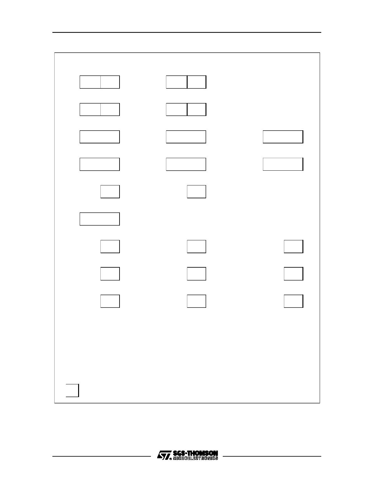
C167 FAMILY PRELIMINARY USER MANUAL
138/180
Figure 38. SFRs and Port Pins Associated with the I/O Ports
VR001914
Port Data Registers
Port Direction Control Registers
Port Open Drain
* Registers in Extended SFR Space
Control Registers
P3.15, P3.13,..P3.0
P2.15..P2.0
P0L.7..0
P0H.7..0
P1L.7..0
P1H.7..0
P0H
P0L
P1H
P1L
P2
P3
DP0H
DP0L
DP1H
DP1L
DP2
DP3
ODP2
ODP3
P4.7..P4.0
P4
DP4
P5
P5.15..P5.0
P6
P6.7..P6.0
P7.7..P7.0
P7
P8.7..P8.0
P8
DP6
DP7
DP8
ODP8
ODP7
ODP6
P0H/P0L
* DP0H/DP0L
P1H/P1L
* DP1H/DP1L
Px
DPx
* ODPx
P5
Port 0 High Byte / Low Byte Data Register
Port 0 High Byte / Low Byte Direction Control Register
Port 1 High Byte / low Byte Data Register
Port 1 High Byte / low Byte Direction Control Register
Port x Data Register (x = 2..4, 6..8)
Port x Direction Control Register (x = 2..4, 6..8)
Port x Open Drain Control Register (x = 2..4, 6..8)
Port 5 Register (Read-Only)

C167 FAMILY PRELIMINARY USER MANUAL
139/180
In the C167, a new feature is implemented in certain ports. The Open Drain Control
allows to switch the output driver of a port pin from a push/pull configuration to an
open drain configuration. In the push/pull configuration, shown on the left in Figure
39, a port output driver has an upper and lower transistor, thus it can actively drive
the line either to a low or a high level. In the open drain mode, illustrated on the right
in Figure 39, the upper transistor is always switched off, and the output driver can
only actively drive the line to a low level. When writing a ’1’ to the port latch, the lower
transistor is switched off and the output goes to a high-impedance state. The high
level must then be performed through an external, user-defined pullup device. With
this feature, it is possible to connect several port pins together through a Wired-AND
configuration, saving external glue logic and/or additional software overhead for
enabling/disabling output signals.
This new feature is implemented for ports P2, P3, P6, P7, and P8 (see respective
sections), and is controlled through respective Open Drain Control Registers ODPx.
These registers allow the individual bit-wise selection of the open drain outputs for
each port line. If the respective control bits ODPx.y is ’0’ (default after reset), the
output driver is in the push/pull mode. If ODPx.y is ’1’, the open drain configuration is
selected. Note that all ODPx registers are located in the ESFR space.
Besides being used as general purpose I/O ports, each port line has one or more
associated alternate function, which serves as an input or output for the bus
controller and/or the on-chip peripheral components. These alternate functions are
also described in the following sections.
To ease the description of a port pin’s configuration in an application, new symbols
have been introduced in this Preliminary User Manual. These symbols are shown in
Figure 39. Instead of showing only the pin symbol when illustrating an alternate input
or output function, an extra block is added to indicate that the entire port structure,
with port latch, direction control, and optional open drain control, has to be
considered when initializing and programming the port line. In this extra block,
besides the pin name, the appropriate configuration of the port line is shown through
arrows. The arrows indicate the direction of the port line, with an output double arrow
symbolizing a push/pull output, and an output single arrow symbolizing an open drain
output, and a single input arrow representing an input.
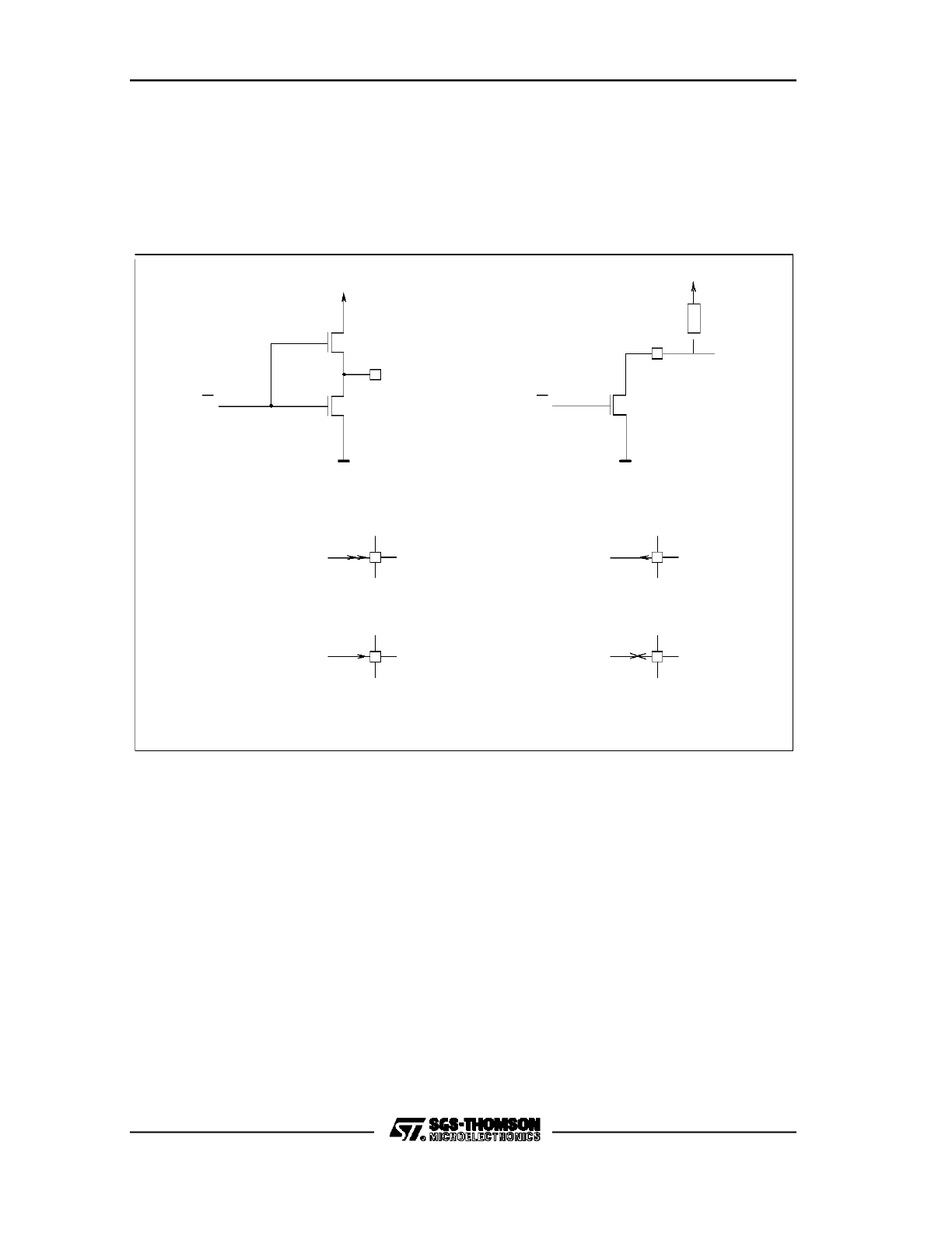
C167 FAMILY PRELIMINARY USER MANUAL
140/180
Sometimes it is necessary in an application, to switch an output off to the high-
impedance mode, in order to avoid external collisions and short circuits. This switch
is performed by setting the direction to input, however, to distinguish it from using
the line as an input, an ’X’ symbol is used in this case. This ’X’ does not indicate a
special mode of the pin, instead, it indicates the idea behind this operation.
Figure 39. Push/Pull and Open Drain Output Drivers / Port Pin Symbols
Q
Push/Pull Output Driver
Open Drain Output Driver
Q
External
Pull-up
Push/Pull Output
Pin Symbol
Pin Symbol
Open Drain Output
Output Driver Switched OFF
Pin Symbol
Pin Symbol
Input
(by Switching Pin to Input)
Push/Pull and Open Drain Output Drivers
Port Pin Symbols
VR001915

C167 FAMILY PRELIMINARY USER MANUAL
141/180
11.0 PORT0: Ports P0L and P0H
In the C167, the 16-bit Port 0 known from the ST10x166 will be split into two 8-bit
ports, named P0L (lower half of former P0), and P0H (upper half). The corresponding
direction registers are then DP0L and DP0H, respectively. These registers and the
associated addresses are shown hereafter. In the description and Figures, however,
the symbol PORT0 is used to refer to both parts, P0L and P0H.
P0L (FF00h/80h)
PORT 0 Low Byte Data Register
Reset Value: 0000h
0
1
2
3
4
5
6
7
P0L5
P0L4
P0L7
P0L6
P0L1
P0L0
P0L3
P0L2
b7 to b0 = P0L.y: Port Data Register y = 0 to 7.
P0H (FF02h/81h)
PORT 0 High Byte Data Register
Reset Value: 0000h
0
1
2
3
4
5
6
7
P0H5
P0H4
P0H7
P0H6
P0H1
P0H0
P0H3
P0H2
b7 to b0 = P0H.y: Port Data Register y = 0 to 7.
DP0L (F100h/80h)
PORT 0 Low Byte Direction Control Register
Reset Value: 0000h
0
1
2
3
4
5
6
7
DP0L5
DP0L4
DP0L7
DP0L6
DP0L1
DP0L0
DP0L3
DP0L2
b7 to b0 = DP0L.y: Direction Control y = 0 to 7.
DP0L.y = 0: Port line P0Ly is input (high impedance).
DP0L.y = 1: Port line P0Ly is output.

C167 FAMILY PRELIMINARY USER MANUAL
142/180
DP0H (F102h/81h)
PORT 0 High Byte Direction Control Register
Reset Value: 0000h
0
1
2
3
4
5
6
7
DP0H5
DP0H4
DP0H7
DP0H6
DP0H1
DP0H0
DP0H3
DP0H2
b7 to b0 = DP0H.y: Direction Control y = 0 to 7.
DP0H.y = 0: Port line P0Hy is input (high impedance).
DP0H.y = 1: Port line P0Hy is output.
This splitting of Port 0 has two advantages for the user. First, when using an 8-bit
demultiplexed bus, only P0L is used for the data bus, and P0H can now be used for
general purpose I/O. This gives the user an extra 8 I/O lines, which are not available
in the ST10x166. Of course, this option is only possible when using the 8-bit
demultiplexed bus exclusively.
The second advantage is with byte writes to a port. Byte moves to an SFR (and a
port is an SFR) cause the not-addressed byte to be cleared. Thus, problems occur
when using the PEC to write a byte to a port (normal instructions could use AND/OR
or bitfield instructions to get around this problem). Now, with Port 0 split into two
bytes, byte write problems are solved.
Although this change is an incompatibility with the ST10x166, minor difficulties are
expected since Port 0 in most cases is currently used as external data bus.
Note that when using an external 16-bit data bus, the two halfs of PORT0 are treated
as one word-wide bus.
The lines of PORT0 are used by the External Bus Controller depending on the
selected bus mode. Figure 40 shows the configuration and alternate functions of
PORT0 in the different modes. It must be noted that the general purpose I/O function
can only be used for pins P0L.0 through P0L.7 if no external bus, and for pins
P0H.0 through P0H.7 if only the 8-bit non-multiplexed bus is used in an
application. While Figure 40 shows four single alternate function configurations of
PORT0, it must be taken into account that in an application mostly several external
bus modes are used.
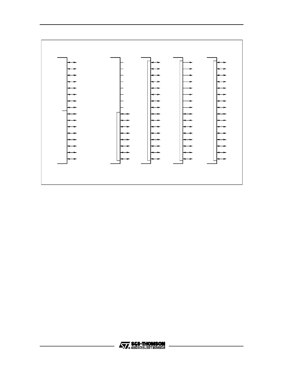
C167 FAMILY PRELIMINARY USER MANUAL
143/180
Figure 40. PORT0 I/O Alternate Functions
P0H.6
P0H.7
PORT 0
P0H.5
P0H.4
P0H.0
P0H.1
P0H.3
P0H.2
P0L.4
P0L.5
P0L.7
P0L.6
P0L.1
P0L.2
P0L.0
P0L.3
P0H
P0L
D3
D0
D2
D1
D6
D7
D5
D4
D4
D5
D7
D6
D1
D2
D0
D3
D11
D8
D10
D9
D14
D15
D13
D12
A12
A13
A15
A14
A9
A10
A8
A11
AD3
AD0
AD2
AD1
AD6
AD7
AD5
AD4
AD4
AD5
AD7
AD6
AD1
AD2
AD0
AD3
AD11
AD8
AD10
AD9
AD14
AD15
AD13
AD12
I/O
a
b
c
d
General Purpose
Alternate Function
8-Bit
Non-MUX Bus
Non-MUX Bus
16-Bit
8-Bit
MUX Bus
16-Bit
MUX Bus
VR001916
PORT0 is also used to select the system startup configuration. During reset, PORT0
is configured to input, and each line is held high through an internal pullup device.
Each line can now be individually pulled to a low level (see DC-level specifications in
the respective Data Sheets) through an external pulldown device. A default
configuration is selected when the respective PORT0 lines are at a high level.
Through pulling individual lines to a low level, this default can be changed according
to the needs of the applications.
The internal pullup devices are designed such that an external pulldown resistors of
about 15 to 20 KOhm (see Data Sheet specification) can be used to apply a correct
low level. These external pulldown resistors can remain connected to the PORT0
pins also during normal operation, however, care has to be taken such that they do
not disturb the normal function of PORT0 (this might be the case, for example, if the
external resistor is too strong).

C167 FAMILY PRELIMINARY USER MANUAL
144/180
With the end of the reset, the selected bus configuration will be written to the
BUSCON0 register. The configuration of the high byte of PORT0, will be copied into
the special register RP0H, shown in Chapter 3.5. This register is read-only, and
holds the selection for the number of chip selects and segment addresses. Software
can read this register in order to react according to the selected configuration, if
required.
When the reset is terminated, the internal pullup devices are switched off, and
PORT0 will be switched to the appropriate operating mode.
11.1 PORT1: Ports P1L and P1H
As with PORT0 described above, also PORT1 known from the ST10x166 is split into
two byte-wide ports in the C167. The registers are P1L, P1H, DP1L, and DP1H
(analogous to the PORT0 registers), shown hereafter.
P1L (FF04h/82h)
PORT 1 Low Byte Data Register
Reset Value: 0000h
0
1
2
3
4
5
6
7
P1L5
P1L4
P1L7
P1L6
P1L1
P1L0
P1L3
P1L2
b7 to b0 = P1L.y: Port Data Register y = 0 to 7.
P1H (FF06h/83h)
PORT 1 High Byte Data Register
Reset Value: 0000h
0
1
2
3
4
5
6
7
P1H5
P1H4
P1H7
P1H6
P1H1
P1H0
P1H3
P1H2
b7 to b0 = P1H.y: Port Data Register y = 0 to 7.
C167 FAMILY PRELIMINARY USER MANUAL
145/180
DP1L (F104h/82h)
PORT 1 Low Byte Direction Control Register
Reset Value: 0000h
0
1
2
3
4
5
6
7
DP1L5
DP1L4
DP1L7
DP1L6
DP1L1
DP1L0
DP1L3
DP1L2
b7 to b0 = DP1L.y: Direction Control y = 0 to 7.
DP1L.y = 0: Port line P1Ly is input (high impedance).
DP1L.y = 1: Port line P1Ly is output.
DP1H (F106h/83h)
PORT 1 High Byte Direction Control Register
Reset Value: 0000h
0
1
2
3
4
5
6
7
DP1H5
DP1H4
DP1H7
DP1H6
DP1H1
DP1H0
DP1H3
DP1H2
b7 to b0 = DP1H.y: Direction Control y = 0 to 7.
DP1H.y = 0: Port line P1Hy is input (high impedance).
DP1H.y = 1: Port line P1Hy is output.
The symbol PORT1 is used to refer to both parts of this port. The upper four pins of
P1H will have additional alternate functions besides the address output in the non-
multiplexed bus modes. These alternate functions are capture inputs of the
CAPCOM2 Unit (see Chapter 5). The relation between the P1H pins and the
alternate functions is as follows:
Pin
Alternate Function
P1H.4
CC24IO CC24 Capture Input
P1H.5
CC25IO CC25 Capture Input
P1H.6
CC26IO CC26 Capture Input
P1H.7
CC27IO CC27 Capture Input
C167 FAMILY PRELIMINARY USER MANUAL
146/180
As all other capture inputs, the capture input function of pins P1H.4 through P1H.7
can also be used as external interrupt inputs (400 ns sample rate @ 20 MHz CPU
clock).
Note that when used as the address bus in the non-multiplexed bus mode, P1L and
P1H are treated as one word-wide port. Either all 16 lines are used for the address
bus, or can be used for general purpose I/O, depending on the bus mode.
As a side effect, the capture input capability of lines P1H.4..7 can also be used in the
address bus mode. With this, one could detect changes of the upper address lines,
and trigger an interrupt request in order to perform some special service routines.
Figure 41 illustrates the I/O and alternate functions of PORT1.
Figure 41. PORT1 I/O and Alternate Functions
P1H.6
P1H.7
PORT 1
P1H.5
P1H.4
P1H.0
P1H.1
P1H.3
P1H.2
P1L.4
P1L.5
P1L.7
P1L.6
P1L.1
P1L.2
P1L.0
P1L.3
P1H
P1L
A12
A13
A15
A14
A1
A10
A9
A11
A4
A0
A3
A2
A7
A8
A6
A5
CC26IO
CC27IO
CC25IO
CC24IO
I/O
a
b
General Purpose
Alternate Function
8/16-Bit
Non-MUX Bus
VR001917
11.2 PORT2
As mentioned in the introduction to the port description, in the C167 Port 2 has an
open drain output feature. The respective control register ODP2 is shown below:
ODP2 (F1C2h/E1h)
Port 2 Open Drain Control Register
Reset Value: 0000h
C167 FAMILY PRELIMINARY USER MANUAL
147/180
ODP2.12
ODP2.11
ODP2.10
ODP2.9
ODP2.8
15
14
13
12
11
10
9
8
0
1
2
3
4
5
6
7
ODP2.5
ODP2.4
ODP2.15
ODP2.14
ODP2.13
ODP2.7
ODP2.6
ODP2.1
ODP2.0
ODP2.3
ODP2.2
b15 to b0 = ODP2.y: Port 2 Open Drain Control bit y = 0 to 15.
ODP2.y = 0: Port 2.y output driver in push / pull mode.
ODP2.y = 1: Port 2.y output driver in open drain mode.
As described in Chapter 10, eight pins of Port 2, pins P2.8 through P2.15, will have
additional alternate functions for the fast external interrupt inputs, while P2.15 also
serves as count input T7IN for timer T7. The following table shows the relationship
between the Port 2 pins and their alternate functions a), b), and c):
Port 2
Pin
Alternate
Function a)
Alternate Function b)
Alternate Function c)
P2.0
CC0IO
P2.1
CC1IO
P2.2
CC2IO
P2.3
CC3IO
P2.4
CC4IO
P2.5
CC5IO
P2.6
CC6IO
P2.7
CC7IO
P2.8
CC8IO
EX0IN
Fast External Interrupt 0 Input
P2.9
CC9IO
EX1IN
Fast External Interrupt 1 Input
P2.10
CC10IO
EX2IN
Fast External Interrupt 2 Input
P2.11
CC11IO
EX3IN
Fast External Interrupt 3 Input
P2.12
CC12IO
EX4IN
Fast External Interrupt 4 Input
P2.13
CC13IO
EX5IN
Fast External Interrupt 5 Input
P2.14
CC14IO
EX6IN
Fast External Interrupt 6 Input
P2.15
CC15IO
EX7IN
Fast External Interrupt 7 Input
T7IN
Timer T7 External Count Input
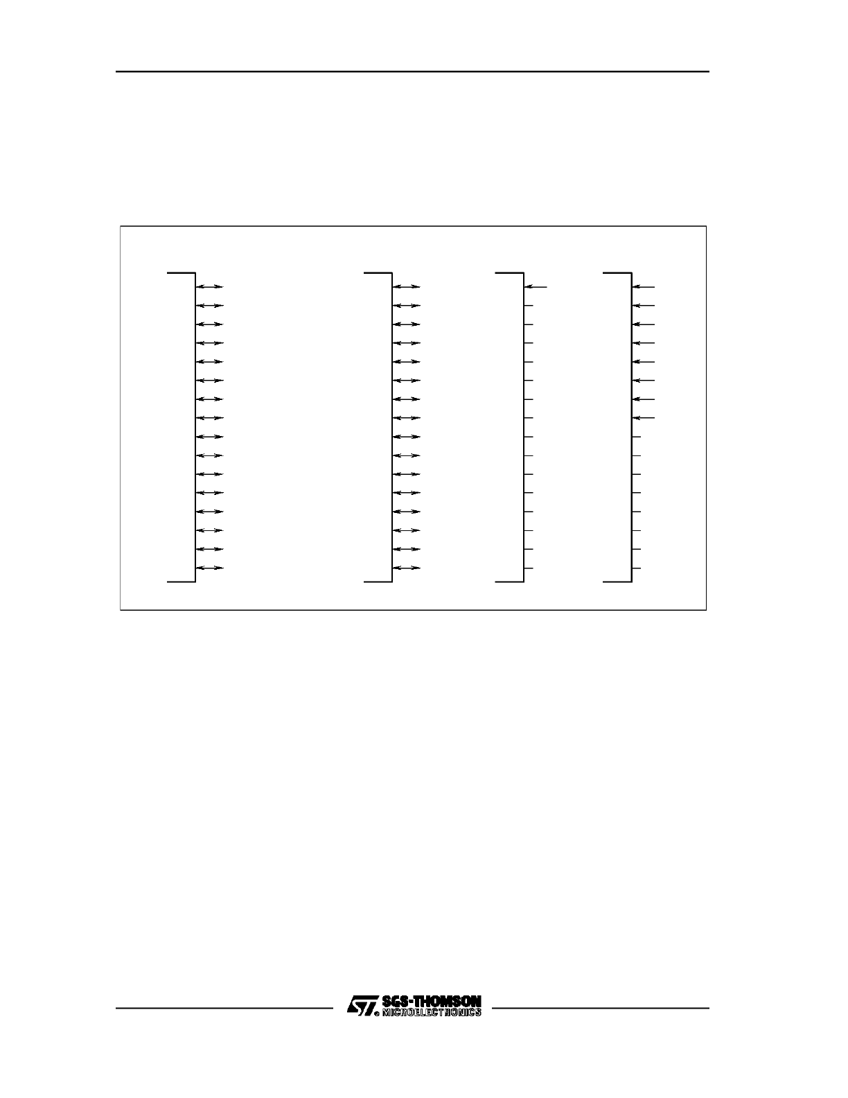
C167 FAMILY PRELIMINARY USER MANUAL
148/180
Figure 42 illustrates the I/O and alternate functions of Port 2.
Note that the second alternate functions of Port 2 pins P2.13 through P2.15 in the
ST10x166, the bus arbitration signals HOLD#, HLDA#, and BREQ#, are now in the
C167 alternate functions of the Port 6 pins P6.5 through P6.7.
Figure 42. PORT2 I/O and Alternate Functions
P2.14
P2.15
PORT 2
P2.13
P2.12
P2.8
P2.9
P2.11
P2.10
P2.4
P2.5
P2.7
P2.6
P2.1
P2.2
P2.0
P2.3
CC4IO
CC5IO
CC7IO
CC6IO
CC1IO
CC2IO
CC0IO
CC3IO
CC11IO
CC8IO
CC10IO
CC9IO
CC14IO
CC15IO
CC13IO
CC12IO
EX3IN
EX2IN
EX1IN
EX6IN
EX7IN
EX5IN
EX4IN
I/O
a
b
c
General Purpose
Alternate Function
VR001918
T7IN
EX0IN
11.3 PORT3
In the C167, the two alternate functions, WR# and READY#, of pins P3.13 and P3.14
in the ST10x166, are performed through dedicated pins. Due to pin limitations in the
target MQFP-144 package, P3.14 will not be connected to a pin. P3.13 received a
new alternate function, which is the clock input/output line SCLK of the Synchronous
Serial Channel, SSC. Pins P3.8 and P3.9, which served for the second
synchronous/asynchronous serial interface ASC1 in the ST10x166, now have the
alternate data in/data out functions of the SSC. The following table shows Port 3 and
the available pins for I/O or alternate functions:

C167 FAMILY PRELIMINARY USER MANUAL
149/180
Port 3
Pin
Alternate Function
P3.0
yes
T0IN
Timer 0 Count Input
P3.1
yes
T6OUT
Timer 6 Toggle Output
P3.2
yes
CAPIN
GPT2 Capture Input
P3.3
yes
T3OUT
Timer 3 Toggle Output
P3.4
yes
T3EUD
Timer 3 External Up/Down Input
P3.5
yes
T4IN
Timer 4 Count Input
P3.6
yes
T3IN
Timer 3 Count Input
P3.7
yes
T2IN
Timer 2 Count Input
P3.8
yes
MTSR
SSC Master Transmit/Slave Receive
P3.9
yes
MRST
SSC Master Receive/Slave Transmit
P3.10
yes
TxD0
ASC0 Transmit Data Output
P3.11
yes
RxD0
ASC0 Receive Data Input
P3.12
yes
BHE#/WRH#
Byte High Enable/Write High Output
P3.13
yes
SCLK
SSC Shift Clock Input/Output
P3.14
no
-----
No Pin assigned in the C167
P3.15
yes
CLKOUT
System Clock Output
With the exception of pins P3.15, P3.14, and P3.12, each line of Port 3 has an open
drain output option. The respective control register ODP3 hereafter. The I/O and
alternate functions of Port 3 are illustrated in Figure 43. The port structures of pins
P3.8/MRST, P3.9/MTSR, and P3.13/SCLK are the same as for P3.11/RxD0
(Alternate Input and Alternate Output Function, see Figure 26).
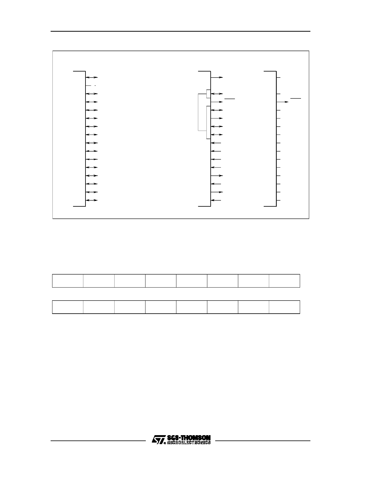
C167 FAMILY PRELIMINARY USER MANUAL
150/180
Figure 43. PORT3 and Alternate Functions
P3.15
PORT 3
P3.13
P3.12
P3.8
P3.9
P3.11
P3.10
P3.4
P3.5
P3.7
P3.6
P3.1
P3.2
P3.0
P3.3
T3EUD
T4IN
T2IN
T3IN
T6OUT
CAPIN
T0IN
T3OUT
RxD0
MRST
TxD0
MTSR
CLKOUT
SCLK
BHE
I/O
a
b
General Purpose
Alternate Function
VR001919
No Pin
WRH
ODP3 (F1C6h/E3h)
Port 3 Open Drain Control Register
Reset Value: 0000h
R
ODP3.11
ODP3.10
ODP3.9
ODP3.8
15
14
13
12
11
10
9
8
0
1
2
3
4
5
6
7
ODP3.5
ODP3.4
R
R
ODP3.13
ODP3.7
ODP3.6
ODP3.1
ODP3.0
ODP3.3
ODP3.2
b15, b14 = R: Reserved.
b12 = R: Reserved.
b13, b11 to b0 = ODP3.y: Port 3 Open Drain Control bit y = 0 to 11, 13.
ODP3.y = 0: Port 3.y output driver in push / pull mode.
ODP3.y = 1: Port 3.y output driver in open drain mode.
C167 FAMILY PRELIMINARY USER MANUAL
151/180
11.4 PORT4
As already mentioned above, Port 4 in the C167 is extended to 8 bits. Registers P4
and DP4 are shown hereafter:
P4 (FFC8h/E4h)
Port 4 Data Register
Reset Value: 0000h
0
1
2
3
4
5
6
7
P4.5
P4.4
P4.7
P4.6
P4.1
P4.0
P4.3
P4.2
b7 to b0 = P4.y: Port 4 Data Register y = 0 to 7.
DP4 (FFCAh/E5h)
Port 4 Direction Control Register
Reset Value: 0000h
0
1
2
3
4
5
6
7
DP4.5
DP4.4
DP4.7
DP4.6
DP4.1
DP4.0
DP4.3
DP4.2
b7 to b0 = DP4.y: Port P4 Direction Control y = 0 to 7.
DP4.y = 0: Port line P4.y is input (high impedance).
DP4.y = 1: Port line P4.y is output.
The pins of Port 4 can either be used as general purpose I/O pins, or they can serve
for the segment addresses A23..A16. The following table lists the Port 4 pins and
their alternate functions:
Port 4
Alternate Function
P4.0
A16
Segment Address Line 16
P4.1
A17
Segment Address Line 17
P4.2
A18
Segment Address Line 18
P4.3
A19
Segment Address Line 19
P4.4
A20
Segment Address Line 20
P4.5
A21
Segment Address Line 21
P4.6
A22
Segment Address Line 22
P4.7
A23
Segment Address Line 23
C167 FAMILY PRELIMINARY USER MANUAL
152/180
The selection between the general purpose I/O function or alternate segment
address function is done during reset (see Chapter 3.5). The selection can be done
in steps of zero (no segment address), two (A17..A16), four (A19..A16), or all eight
port lines (A23..A16). As an example, when selecting 4 segment address lines, Port
4 pins P4.0 through P4.3 will be used for the segment address, and lines P4.4
through P4.7 can be used for general purpose I/O. The table below illustrates these
options:
Port 4
Selected Number of Segment Address Lines
0
2
4
8
P4.0
P4.1
P4.2
P4.3
P4.4
P4.5
P4.6
P4.7
I/O
I/O
I/O
I/O
I/O
I/O
I/O
I/O
A16
A17
I/O
I/O
I/O
I/O
I/O
I/O
A16
A17
A18
A19
I/O
I/O
I/O
I/O
A16
A17
A18
A19
A20
A21
A22
A23
Figure 44 illustrates the I/0 and alternate functions of Port 4. The shaded bars in the
Figure indicate that the alternate function is selected in groups.
Figure 44. PORT4 I/O and Alternate Functions
PORT 4
I/O
General Purpose
Alternate Function
VR001920
P4.7
P4.6
P4.5
P4.0
P4.1
P4.2
P4.3
P4.4
A20
A19
A18
A17
A16
A21
A22
A23
The number of segment address lines selected during reset can be read in register
RP0H (see Chapter 3.5). Bits 3 and 4 of this register reflect the bit combination which
was read during reset at the P0H pins 3 and 4 (see Table 3.5). These bits are read-
only, and can be used to check the selected configuration during run-time.
C167 FAMILY PRELIMINARY USER MANUAL
153/180
The input/output structure of the new additional Port 4 pins is the same as for pins
P4.0 and P4.1, described in the ST10 User Manual, Chapter 10.1.4. The only
difference to the ST10x166’s Port 4 operation is that the automatic switch of the
alternate output function will only be performed for the pins selected for segment
address function.
11.5 PORT5
Port 5 will be extended to 16 pins, shown hereafter. The Port 5 lines can either be
used as analog input channels for the A/D converter, or as digital input-only lines.
The upper six pins of Port 5 have additional alternate input functions for the GPT1
and GPT2 timers. Figure 45 illustrates the input and alternate input functions of Port
5. For more details on the Port 5 pins please refer to the ST10 User Manual, Chapter
10.2.
Figure 45. PORT5 Input and Alternate Functions
P5.15
PORT 5
P5.13
P5.12
P5.8
P5.9
P5.11
P5.10
P5.4
P5.5
P5.7
P5.6
P5.1
P5.2
P5.0
P5.3
I/O
a
b
General Purpose
Alternate Function
VR001921
P5.14
AN14
AN3
AN0
AN2
AN1
AN6
AN7
AN5
AN4
AN10
AN11
AN9
AN8
AN12
AN13
AN15
T2EUD
T5IN
T6IN
T5EUD
T6EUD
T4EUD
P5 (FFA2h/D1h)
Port 5 Data Register (Read Only)
Reset Value: xxxxh
C167 FAMILY PRELIMINARY USER MANUAL
154/180
P5.12
P5.11
P5.10
P5.9
P5.8
15
14
13
12
11
10
9
8
0
1
2
3
4
5
6
7
P5.5
P5.4
P5.15
P5.14
P5.13
P5.7
P5.6
P5.1
P5.0
P5.3
P5.2
b0 to B15 = P5.y: Port 5 Data Register y= 0 to 15.
11.6 PORT6
Port 6 is an 8-bit bidirectional general purpose I/O port. Each port line is bit
addressable, and can individually be programmed for input or output via the direction
control register DP6. The open drain output option is available for Port 6. The
registers of Port 6 are shown hereafter:
P6 (FFCCh/E6h)
Port 6 Data Register
Reset Value: 0000h
0
1
2
3
4
5
6
7
P6.5
P6.4
P6.7
P6.6
P6.1
P6.0
P6.3
P6.2
b7 to b0 = P6.y: Port 6 Data Register y = 0 to 7.
DP6 (FFCEh/E7h)
Port 6 Direction Control Register
Reset Value: 0000h
0
1
2
3
4
5
6
7
DP6.5
DP6.4
DP6.7
DP6.6
DP6.1
DP6.0
DP6.3
DP6.2
b7 to b0 = DP6.y: Port P6 Direction Control y = 0 to 7.
DP6.y = 0: Port line P6.y is input (high impedance).
DP6.y = 1: Port line P6.y is output.
C167 FAMILY PRELIMINARY USER MANUAL
155/180
ODP6 (F1CEh/E7h)
Port 6 Open Drain Control Register
Reset Value: 0000h
0
1
2
3
4
5
6
7
ODP6.5
ODP6.4
ODP6.7
ODP6.6
ODP6.1
ODP6.0
ODP6.3
ODP6.2
b7 to b0 = ODP6.y: Port P6 Open Drain Control y = 0 to 7.
ODP6.y = 0: Port P6.y is output driver in push / pull mode.
ODP6.y = 1: Port P6.y is output driver in open drain mode.
All lines of Port 6 can also be used for alternate functions, shown in the following:
Port 6
Alternate Function
P6.0
CS0#
Chip Select 0 Output (BUSCON0)
P6.1
CS1#
Chip Select 1 Output (BUSCON1)
P6.2
CS2#
Chip Select 2 Output (BUSCON2)
P6.3
CS3#
Chip Select 3 Output (BUSCON3)
P6.4
CS4#
Chip Select 4 Output (BUSCON4)
P6.5
HOLD#
External Hold Request Input
P6.6
HLDA#
Hold Acknowledge Output
P6.7
BREQ#
Bus Request Output
The selection between the I/O function and the alternate chip select function is done
during reset (see Chapter 3.5). Either zero, two (CS0# and CS1#), three (CS0#,
CS1#, and CS2#), or all five chip select outputs can be selected. The remaining pins
can be used for general purpose I/O. The table below shows these options:
Port 6
Selected Number of Chip Select Signals
0
2
3
5
P6.0
P6.1
P6.2
P6.3
P6.4
I/O
I/O
I/O
I/O
I/O
CS0#
CS1#
I/O
I/O
I/O
CS0#
CS1#
CS2#
I/O
I/O
CS0#
CS1#
CS2#
CS3#
CS4#

C167 FAMILY PRELIMINARY USER MANUAL
156/180
The chip select lines of Port 6 additionally have an internal weak pullup device. This
device is switched on under the following conditions:
-
always during reset
-
if the Port 6 line is used as a chip select output, and the C167 is in the Hold mode
(invoked through HOLD#), and the respective ODP6.x control bit is ’0’.
This feature is implemented in order to have the chip select lines high during reset, in
order to avoid multiple chip selection, and to allow another master to access the
external memory via the same chip select lines (Wired-AND), while the C167 is in the
Hold mode. With ODP6.x = 1 (open drain output selected), the internal pullup device
will not be active during the Hold mode; external user-defined pullup devices must be
used in this case anyway.
The number of chip select lines selected during reset can be read in register RP0H.
Bits 1 and 2 of this register reflect the bit combination which was read during reset at
the P0H pins 1 and 2 (see Chapter 3.5 and Table 3.5). These bits are read-only, and
can be used to check the selected configuration during run-time.
Figure 46 shows a block diagram of a Port 6 pin used for the chip selects
(P6.4..P6.0). Since the chip select signals are required directly after reset, the pins
selected during reset for this function are switched automatically to the alternate
output function. It has to be taken into account, however, that the open drain output
option can only be selected through software earliest during the initialization routine;
at least signal CS0# will be in the push/pull output driver mode directly after reset.
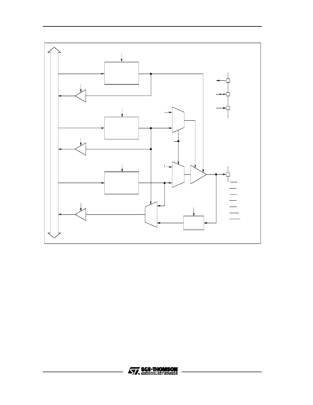
C167 FAMILY PRELIMINARY USER MANUAL
157/180
Figure 46. Block Diagram of a PORT6 Pin (P6.7, P6.6, P6.4..P6.0)
VR0M1643
X
U
M
0
1
Latch
Open Drain
Input
Latch
Write ODP6.y
Read ODP6.y
Read P6.y
Output
Buffer
Write DP6.y
I
n
t
e
r
n
a
l
B
u
s
Clock
P6.0/CS0
P6.1/CS1
P6.2/CS2
ODP6.y
DP6.y
Direction
Latch
Read DP6.y
Latch
Port Output
P6.y
Write P6.y
Alternate
Output
Input
Push/Pull
Output
Open Drain
Output
P6.y
Symbols
0
M
U
X
1
Data
1
X
U
M
0
Alternate
Function
Enable
’1’
P6.y
P6.y
P6.6/HLDA
P6.4/CS4
P6.3/CS3
P6.7/BREQ
y = (0...4, 6, 7)
The bus arbitration signals HOLD#, HLDA#, and BREQ# are selected with bit
HLDEN in register PSW. Please refer to the ST10 User Manual for details on these
pin functions. Figure 46 also represents the block diagram of the Port 6 pins used for
Hold Acknowledge, HLDA#, and Bus Request, BREQ# (P6.7, P6.6). When the bus
arbitration signals are enabled via HLDEN, also these pins are switched
automatically to the appropriate direction. Figure 48 shows the port structure of the
P6.5/HOLD# pin.
Figure 47 illustrates the I/O and alternate functions of Port 6. Again, a shaded bar
indicates that these functions can only be selected in groups.
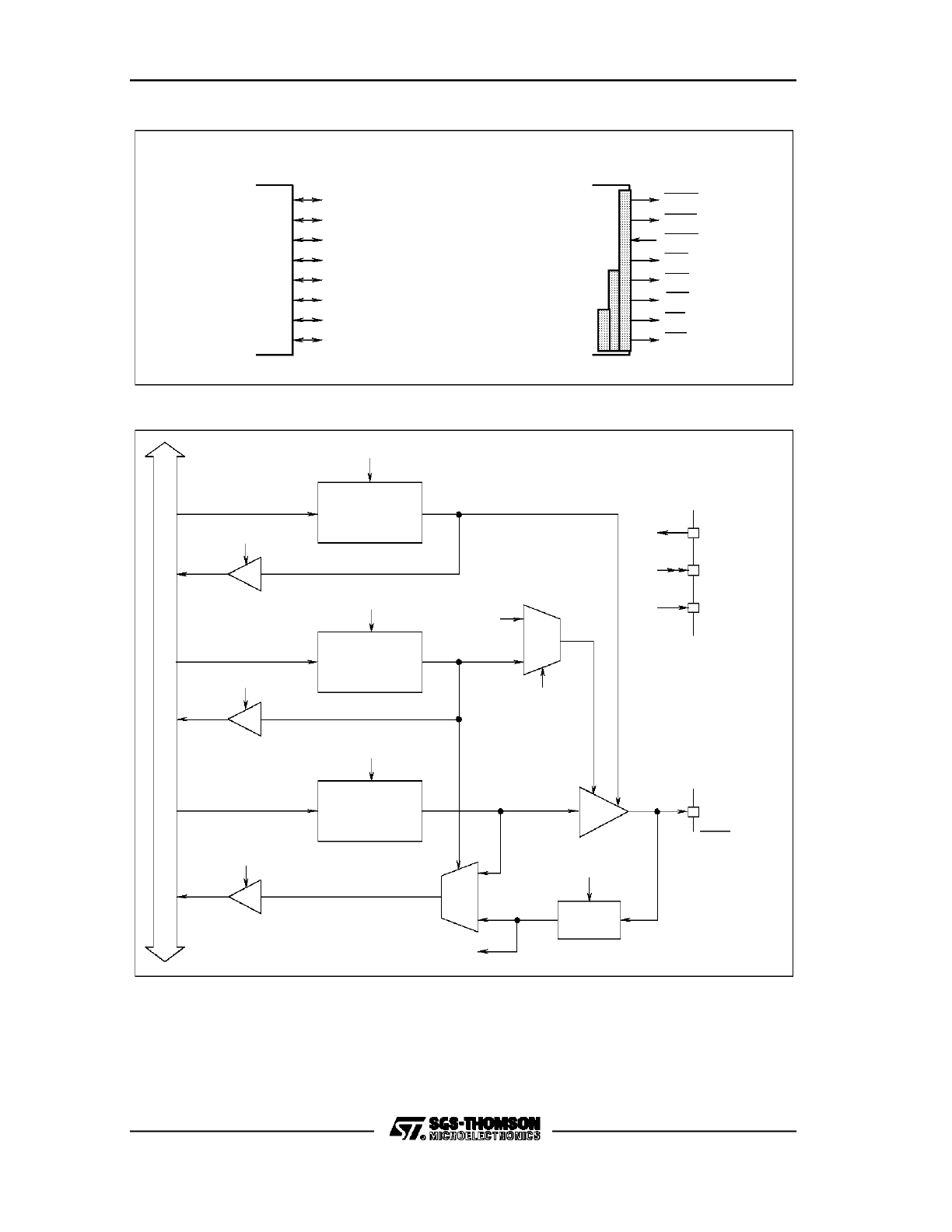
C167 FAMILY PRELIMINARY USER MANUAL
158/180
Figure 47. PORT6 I/O Alternate Functions
PORT 6
I/O
General Purpose
Alternate Function
VR001922
P6.7
P6.6
P6.5
P6.0
P6.1
P6.2
P6.3
P6.4
CS4
CS3
CS2
CS1
CS0
HOLD
HLDA
BREQ
Figure 48. Block Diagram of the PORT6 Pin P6.5, HOLD#
VR0N1643
X
U
M
0
1
Latch
Open Drain
Input
Latch
Write ODP6.5
Read ODP6.5
Read P6.5
Output
Buffer
Write ODP6.5
I
n
t
e
r
n
a
l
B
u
s
Clock
P6.5/HOLD
ODP6.5
DP6.5
Direction
Latch
Read DP6.5
Latch
Port Output
P6.5
Write P6.5
Input
Push/Pull
Output
Open Drain
Output
P6.5
Symbols
1
X
U
M
0
Alternate
Function
Enable
’0’
Alternate
Data Input
P6.5
P6.5

C167 FAMILY PRELIMINARY USER MANUAL
159/180
11.7 PORT7
Port 7 is an 8-bit bidirectional general purpose I/O port. Each port line is bit-
addressable, and can individually be programmed for input or output via the direction
control register DP7. The open drain output option is available for Port 7. Herebelow
are shown registers P7, DP7, and ODP7.
P7 (FFD0h/E8h)
Port 7 Data Register
Reset Value: 0000h
0
1
2
3
4
5
6
7
P7.5
P7.4
P7.7
P7.6
P7.1
P7.0
P7.3
P7.2
b7 to b0 = P7.y: Port 7 Data Register y = 0 to 7.
DP7 (FFD2h/E9h)
Port 7 Direction Control Register
Reset Value: 0000h
0
1
2
3
4
5
6
7
DP7.5
DP7.4
DP7.7
DP7.6
DP7.1
DP7.0
DP7.3
DP7.2
b7 to b0 = DP7.y: Port P7 Direction Control y = 0 to 7.
DP7.y = 0: Port line P7.y is input (high impedance).
DP7.y = 1: Port line P7.y is output.
ODP7 (F1D2h/E9h)
Port 7 Open Drain Control Register
Reset Value: 0000h
0
1
2
3
4
5
6
7
ODP7.5
ODP7.4
ODP7.7
ODP7.6
ODP7.1
ODP7.0
ODP7.3
ODP7.2
b7 to b0 = ODP7.y: Port P7 Open Drain Control y = 0 to 7.
ODP7.y = 0: Port P7.y is output driver in push / pull mode.
ODP7.y = 1: Port P7.y is output driver in open drain mode.

C167 FAMILY PRELIMINARY USER MANUAL
160/180
All lines of Port 7 can also be used for alternate functions of the PWM module and
the CAPCOM2 Unit, as follows:
Port 7
Alternate Function
P7.0
POUT0
PWM Channel 0 Output
P7.1
POUT1
PWM Channel 1 Output
P7.2
POUT2
PWM Channel 2 Output
P7.3
POUT3
PWM Channel 3 Output
P7.4
CC28IO
CC28 Capture Input/Compare Output
P7.5
CC29IO
CC29 Capture Input/Compare Output
P7.6
CC30IO
CC30 Capture Input/Compare Output
P7.7
CC31IO
CC31 Capture Input/Compare Output
The port structure of pins P7.0 through P7.3 is similar to the structure of Port 3 pins
with an alternate output function (e.g. T3OUT, T6OUT, etc.), as it is described in the
ST10 User Manual, Chapter 10.1.3.2. The exception is, however, that the port output
latch value and the alternate data output are not ANDed, but EXORed. This feature
allows to invert the alternate output by writing a ’1’ into the respective output latch.
With a ’0’ in the port latch, the alternate output is not inverted. With this option,
however, separate alternate output enable control bits must be provided (i.e. PENx in
register PWMCON1). Figure 49 shows a block diagram of a P7 pin (P7.0 through
P7.3).
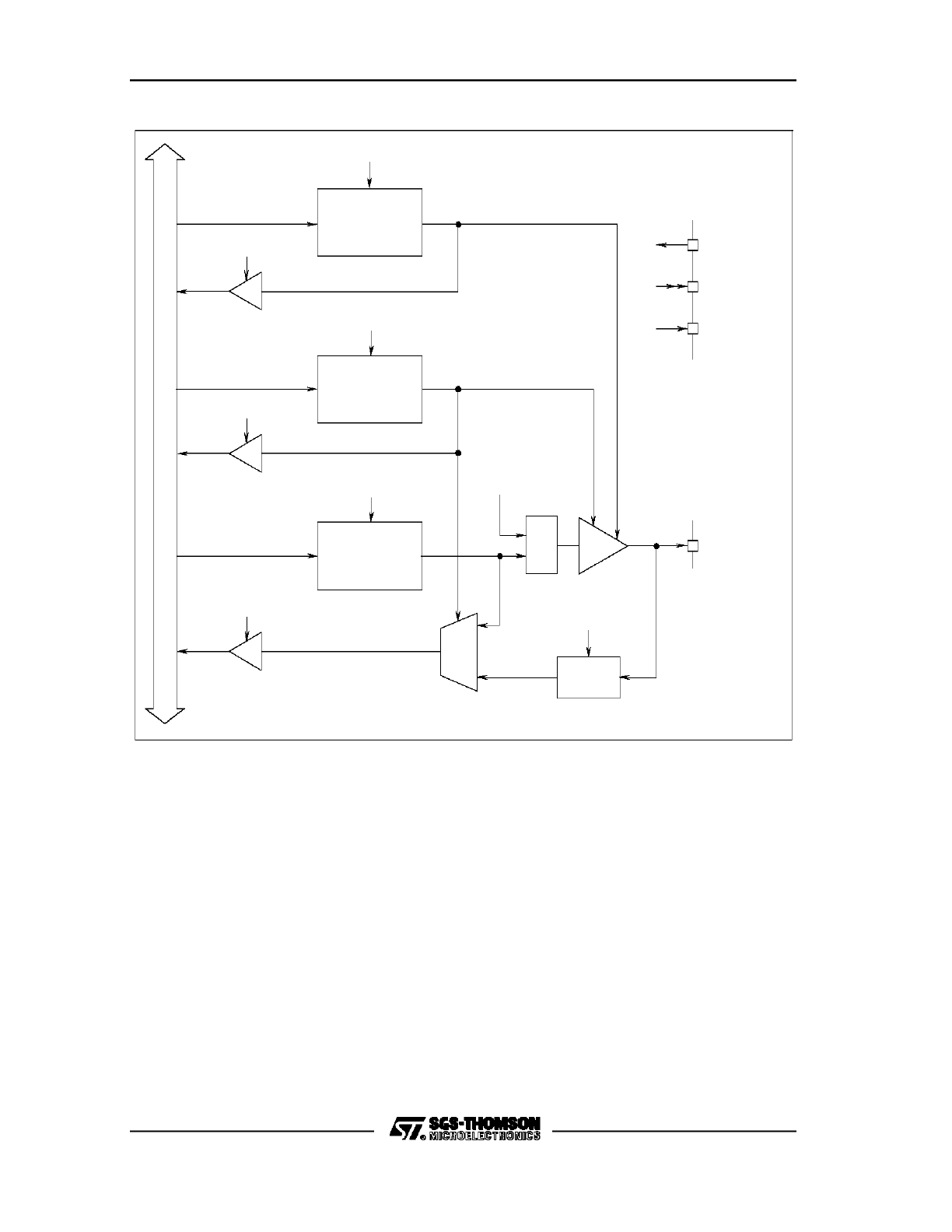
C167 FAMILY PRELIMINARY USER MANUAL
161/180
Figure 49. Block Diagram of a PORT7 Pin (P7.3..P7.0)
VR0P1643
X
U
M
0
1
Latch
Open Drain
Input
Latch
Write ODP7.y
Read ODP7.y
Read P7.y
Output
Buffer
Write DP7.y
I
n
t
e
r
n
a
l
B
u
s
Clock
P7.y/POUTy
ODP7.y
DP7.y
Direction
Latch
Latch
Port Output
P7.y
Write P7.y
Alternate
Data Output
=1
Input
Push/Pull
Output
Open Drain
Output
P7.y
Symbols
Read DP7.y
P7.y
P7.y
EXOR
y = (0...3)
The port structure of pins P7.4 through P7.7 is the same as for the pins of Port 2, and
is shown in Figure 50. For a detailled description please refer to Chapter 10.1.2 of
the ST10 User Manual.
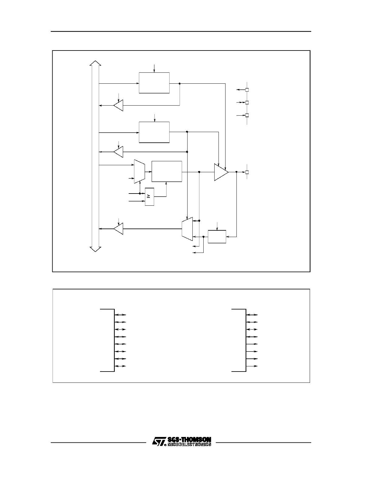
C167 FAMILY PRELIMINARY USER MANUAL
162/180
Figure 50. Block Diagram of a PORT7 Pin (P7.7..P7.4)
VR0Q1643
X
U
M
0
1
Latch
Open Drain
Input
Latch
Write ODP7.y
Read ODP7.y
Read P7.y
Output
Buffer
Write DP7.y
I
n
t
e
r
n
a
l
B
u
s
Clock
P7.y/CCzIO
ODP7.y
DP7.y
Direction
Latch
Read DP7.y
Latch
Port Output
P7.y
Input
Push/Pull
Output
Open Drain
Output
P7.y
Symbols
0
M
U
X
1
z = (28...31)
Alternate
Data Output
Write P7.y
Compare
Trigger
1
Alternate Latch Data Input
Alternate Pin Data Input
y = (4...7)
P7.y
P7.y
Figure 51. PORT7 I/O and Alternate Functions
PORT 7
I/O
General Purpose
Alternate Function
VR001923
P7.7
P7.6
P7.5
P7.0
P7.1
P7.2
P7.3
P7.4
CC28IO
POUT3
POUT2
POUT1
POUT0
CC29IO
CC30IO
CC31IO
11.8 PORT8

C167 FAMILY PRELIMINARY USER MANUAL
163/180
Port 8 is an 8-bit bidirectional general purpose I/O port. Each port line is bit-
addressable, and can individually be programmed for input or output via the direction
control register DP8. The open drain output option is available also for Port 8.
Registers P8, DP8, and ODP8 are shown herebellow :
P8 (FFD4h/EAh)
Port 8 Data Register
Reset Value: 0000h
0
1
2
3
4
5
6
7
P8.5
P8.4
P8.7
P8.6
P8.1
P8.0
P8.3
P8.2
b7 to b0 = P8.y: Port 8 Data Register y = 0 to 7.
DP8 (FFD6h/EBh)
Port 8 Direction Control Register
Reset Value: 0000h
0
1
2
3
4
5
6
7
DP8.5
DP8.4
DP8.7
DP8.6
DP8.1
DP8.0
DP8.3
DP8.2
b7 to b0 = DP8.y: Port P8 Direction Control y = 0 to 7.
DP8.y = 0: Port line P8.y is input (high impedance).
DP8.y = 1: Port line P8.y is output.
ODP8 (F1D6h/EBh)
Port 8 Open Drain Control Register
Reset Value: 0000h
0
1
2
3
4
5
6
7
ODP8.5
ODP8.4
ODP8.7
ODP8.6
ODP8.1
ODP8.0
ODP8.3
ODP8.2
b7 to b0 = ODP7.y: Port P7 Open Drain Control y = 0 to 7.
ODP7.y = 0: Port P7.y is output driver in push / pull mode.
ODP7.y = 1: Port P7.y is output driver in open drain mode.
All lines of Port 8 can be used for the alternate compare output/capture input
functions of registers CC16 through CC23 of the CAPCOM2 Unit:
Port 8
Alternate Function

C167 FAMILY PRELIMINARY USER MANUAL
164/180
P8.0
P8.1
P8.2
P8.3
P8.4
P8.5
P8.6
P8.7
CC16IO
CC16 Capture Input/Compare Output
CC17IO
CC17 Capture Input/Compare Output
CC18IO
CC18 Capture Input/Compare Output
CC19IO
CC19 Capture Input/Compare Output
CC20IO
CC20 Capture Input/Compare Output
CC21IO
CC21 Capture Input/Compare Output
CC22IO
CC22 Capture Input/Compare Output
CC23IO
CC23 Capture Input/Compare Output
The port input/output buffer structure of the pins of Port 8 is the same as for the pins
of Port 2. Figure 52 shows a block diagram of a Port 8 pin. For a detailled description
please refer to Chapter 10.1.2 of the ST10 User Manual.
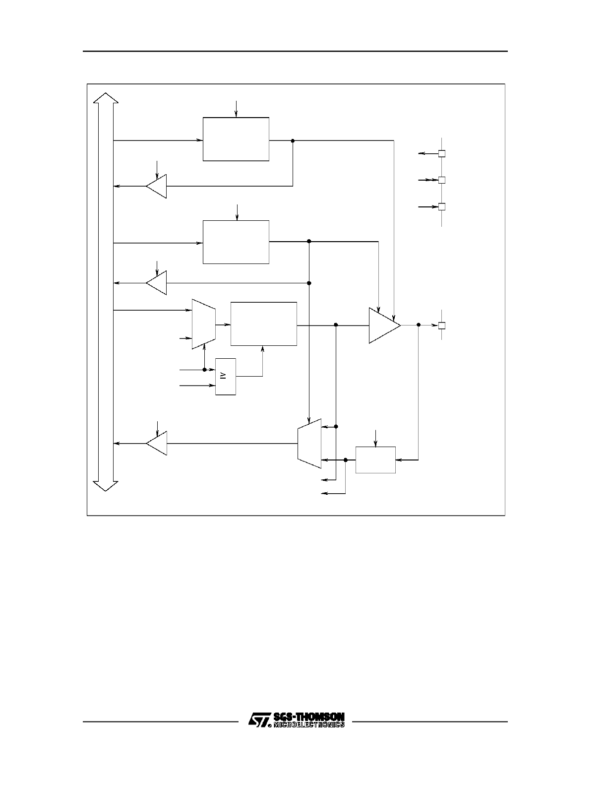
C167 FAMILY PRELIMINARY USER MANUAL
165/180
Figure 52. Block Diagram of a PORT8 Pin
VR0R1643
X
U
M
0
1
Latch
Open Drain
Input
Latch
Write ODP8.y
Read ODP8.y
Read P8.y
Output
Buffer
Write DP8.y
I
n
t
e
r
n
a
l
B
u
s
Clock
P8.y/CCzIO
ODP8.y
DP8.y
Direction
Latch
Read DP8.y
Latch
Port Output
P8.y
Input
Push/Pull
Output
Open Drain
Output
P8.y
Symbols
0
M
U
X
1
z = (16...23)
Alternate
Data Output
Write P8.y
Compare
Trigger
1
Alternate Latch Data Input
Alternate Pin Data Input
y = (0...7)
P8.y
P8.y
C167 FAMILY PRELIMINARY USER MANUAL
166/180
Figure 53. PORT8 I/O and Alternate Functions
PORT 8
I/O
General Purpose
Alternate Function
VR0A1923
P8.7
P8.6
P8.5
P8.0
P8.1
P8.2
P8.3
P8.4
CC20IO
CC19IO
CC18IO
CC17IO
CC16IO
CC21IO
CC22IO
CC23IO

C167 FAMILY PRELIMINARY USER MANUAL
167/180
12.
DEDICATED PINS
A number of pins of the C167 are dedicated to specific functions. These pins are
listed in the following:
Pin
Function
ALE
Address Latch Enable
RD#
External Memory Read Strobe
WR#/WRL#
External Memory Write/Write Low Strobe
READY#
Ready Input
EA#
External Access Enable
NMI#
Non-Maskable Interrupt Input
RSTIN#
Reset Input
RSTOUT#
Reset Output
XTAL1/2
Oscillator Input/Output
VAREF/VAGND
Analog Power Supply
VPP
Reserved
VCC/VSS
Digital Power Supply (20 Pins total)
There is a total of 33 dedicated pins. Figure 54 gives an overview on these pins.
Other than in the ST10x166, the WR#/WRL# pin is no more an alternate function,
thus, there is no external pullup device necessary in order to apply a high level to this
line during the initialization procedure. This is now a push/pull output during normal
operation, and is held high through an internal pullup device during reset.
C167 FAMILY PRELIMINARY USER MANUAL
168/180
Figure 54. Dedicated Pins and Alternate Functions
ALE
Dedicated
WR
READY
RSTOUT
RSTIN
EA
NMI
VAGND
VAREF
XTAL1
XTAL2
V
I/O
General Purpose
Alternate Function
VR001924
RD
Pins
PP
CC
V
SS
V
(reserved)
(10)
(10)
WRL

C167 FAMILY PRELIMINARY USER MANUAL
169/180
13.
PINOUT
The following table gives a pin description of the ST10167
Symbol
Pin
Number
Input
(I)
Output
(O)
Function
XTAL1
XTAL2
138
137
I
O
Input to the oscillator amplifier and input to the external clock
generator.
Output of the oscillator amplifier circuit.
To drive the device from an external source, XTAL1 should be driven
while XTAL2 is left unconnected. Minimum and maximum high/ low
and rise/fall times specified in the AC characteristics must be
observed.
RSTIN#
140
I
Reset input with Schmitt-Trigger characteristics. A low level at this
pin for a specified duration while the oscillator is running resets the
C167. An internal pullup resistor permits power-on reset using only a
capacitor connected to Vss.
RSTOUT#
141
O
Internal Reset Indication Output. This pin is set to a low level when
the part is executing eiter a hardware-, a software- or a watchdog
timer reset. RSTOUT# remains low until the EINIT (end of
initialization) instruction is executed.
NMI#
142
I
Non-Maskable Interrupt Input. A high to low transition at this pin
causes the CPU to vector the NMI trap routine. When the PWRDN
(power down) instruction is executed, the NMI# pin must be low in
order to force the C167 to go into power down mode. If NMI# is high
when PWRDN is executed, the part will continue to run in normal
mode.
ALE
98
O
Address Latch Enable Output. Can be used for latching the address
into external memory or an address latch in the multiplexed bus
modes.
RD#
95
O
External Memory Read Strobe. RD# is activated for every external
instruction or data read access.
WR#/ WRL#
96
O
External Memory Write Strobe. This pin has two modes of operation,
selected through WRCFG in register SYSCON: In the WR# mode,
this pin is activated for every external data write access. In the WRL#
mode, this pin is activated for every low byte write access for 16-bit
data busses, and for every byte write access for 8-bit busses. In this
mode, this pin is used together with pin BHE#/WRH#, which
indicates every external high byte write access.
READY#
97
I
Ready Input. When the Ready function is enabled, a high level at this
pin during an external memory access will force the insertion of
memory cycle time waitstates until the pin returns to a low level.
EA#
99
I
External Access Enable pin. A low level at this pin during and after
reset forces the C167 to begin instruction execution out of external
memory. A high level forces execution out of the internal ROM. For
ROMless versions, this pin must be tied to ’0’.

C167 FAMILY PRELIMINARY USER MANUAL
170/180
Symbol
Pin
Number
Input
(I)
Output
(O)
Function
PORT0:
P0L.0 - P0L.7
P0H.0 - P0H.7
100 - 107
108,
111 - 117
I/O
PORT0 consists of the two 8-bit bidirectional I/O ports P0L and P0H.
They are bit-wise programmable for input or output via a direction bit.
For a pin configured as input, the output driver is put into high-
impedance state.
In case of an external bus configuration, PORT0 serves as the
address and address/data bus in the multiplexed bus modes and as
the data bus in the non-multiplexed bus modes.
Non-Multiplexed Bus Modes:
Data Width:
8-Bit
16-Bit
P0L.0 - P0L.7
D0 - D7
D0 - D7
P0H.0 - P0H.7
I/O
D8 - D15
Multiplexed Bus Modes:
Data Width:
8-Bit
16-Bit
P0L.0 - P0L.7
AD0 - AD7 AD0 - AD7
P0H.0 - P0H.7
A8 - A15
AD8 - AD15
PORT1:
P1L.0 - P1L.7
P1H.0 - P1H.7
118 - 125
128 - 135
I/O
I
I
I
I
PORT1 consists of the two 8-bit bidirectional I/O ports P1L and P1H.
They are bit-wise programmable for input or output via a direction bit.
For a pin configured as an input, the output driver is put into high-
impedance state.
PORT1 is also used as the 16 bit address bus (Ax) in the non-
multiplexed bus modes. In this mode, P1L and P1H are treated as
one word- wide port.
Four lines of P1H are also used for alternate functions of the
CAPCOM2 Unit:
P1H.7
CC27IO
CAPCOM2 Reg. CC27 Capture Input
P1H.7
CC26IO
CAPCOM2 Reg. CC26 Capture Input
P1H.7
CC25IO
CAPCOM2 Reg. CC25 Capture Input
P1H.7
CC24IO
CAPCOM2 Reg. CC24 Capture Input
P2.0 - P2.15
47 - 54
57 - 64
I/O
I/O
...
I/O
I/O
I
...
I/O
I
I
Port 2 is a 16-bit bidirectional I/O port. It is bit-wise programmable for
input or output via a direction bit, and the output drivers can be
switched into push/pull or open drain operation. For a pin configured
as input, the output driver is put into high impedance state.
The pins of Port 2 are also used for different alternate functions for
the CAPCOM Units and for fast external interrupt inputs:
P2.0
CC0IO
CAPCOM Register CC0 Cap. In/Comp. Out
. . .
P2.7
CC7IO
CAPCOM Register CC7 Cap. In/Comp. Out
P2.8
CC8IO
CAPCOM Register CC8 Cap. In/Comp. Out
EX0IN
Fast External Interrupt 0 Input
. . .
P2.15
CC15IO CAPCOM Reg. CC15 Cap. In/Com. Out
EX7IN
Fast External Interrupt 7 Input
T7IN
CAPCOM2 Timer T7 Count Input

C167 FAMILY PRELIMINARY USER MANUAL
171/180
Symbol
Pin
Number
Input
(I)
Output
(O)
Function
P3.0 - P3.13,
P3.15
65 - 70,
73 - 80,
81
I/O
I
O
I
O
I
I
I
I
I/O
I/O
O
I
I/O
O
O
I/O
O
Port 3 is a 16-bit bidirectional I/O port. It is bit-wise programmable for
input or output via a direction bit, and the output drivers can be switched
into push/pull or open drain operation. For a pin configured as input, the
output driver is put into high-impedance state.
The pins of Port 3 are also used for various functions as timer inputs and
outputs and bus control signals:
P3.0
T0IN
CAPCOM Timer T0 Count Input
P3.1
T6OUT
GPT2 Timer T6 Toggle Latch Output
P3.2
CAPIN
GPT2 Register CAPREL Capture Input
P3.3
T3OUT
GPT1 Timer T3 Toggle Latch Output
P3.4
T3EUD
GPT1 Timer T3 External Up/Down Control Input
P3.5
T4IN
GPT1 Timer T4 Count/Capture/Reload Input
P3.6
T3IN
GPT1 Timer T3 Count Input
P3.7
T2IN
GPT1 Timer T2 Count/Capture/Reload Input
P3.8
MRST
SSC Master Receive/Slave Transmit In./Out.
P3.9
MTSR
SSC Master Transmit/Slave Receive Out./In.
P3.10
TxD0
ASC0 Data Output/Clock Output (Async./Sync)
P3.11
RxD0
ASC0 Data Input (Async.)
Data Input/Output (Sync.)
P3.12
BHE#
External Memory High Byte Enable Signal
WRH#
External Memory High Byte Write Strobe
P3.13
SCLK
SSC Master Clock Output/Slave Clock Input
P3.15
CLKOUT
System Clock Output (= CPU Clock)
P4.0 - P4.7
85 - 92
I/O
O
...
O
Port 4 is a 8- bit bidirectional I/O port. It is bitwise programmable for
input or output via a direction bit. For a pin configured as input, the
output driver is put into high-impedance state.
In case of an external bus configuration, the lines of Port 4 can be
used for output of the segment address lines:
P4.0
A16
Least Significant Segment Address Line
. . .
P4.7
A23
Most Significant Segment Address Line
P5.0 - P5.15
27 - 36
39 - 44
I
I
...
I
I
I
I
I
I
I
Port 5 is a 16-bit input-only port with Schmitt-Trigger characteristics.
The pins of Port 5 are also used as the analog inputs to the A/D
converter, and for timer inputs:
P5.0
AN0
Analog Input 0
. . .
P5.15
AN15
Analog Input 15
P5.10
T6EUD
GPT2 Timer T6 External Up/Down Control Input
P5.11
T5EUD
GPT2 Timer T5 External Up/Down Control Input
P5.12
T6IN
GPT2 Timer T6 Count Input
P5.13
T5IN
GPT2 Timer T5 Count Input
P5.14
T4EUD
GPT1 Timer T4 External Up/Down Control Input
P5.15
T2EUD
GPT1 Timer T4 External Up/Down Control Input
VAREF
37
A/D converter analog reference voltage
VAGND
38
A/D converter analog reference ground

C167 FAMILY PRELIMINARY USER MANUAL
172/180
Symbol
Pin
Number
Input
(I)
Output
(O)
Function
P6.0 - P6.7
1 - 8
I/O
O
...
O
I
O
O
Port 6 is an 8 bit bidirectional I/O port. It is bit-wise programmable for
input or output via a direction bit, and the output drivers can be
switched into push/pull or open drain operation. For a pin configured
as input, the output driver is put into high-impedance state.
The pins of Port 6 are also used for various alternate functons:
P6.0
CS0#
Chip Select 0 Output
. . .
P6.4
CS4#
Chip Select 4 Output
P6.5
HOLD#
External Master Hold Request Input
P6.6
HLDA#
Hold Acknowledge Output
P6.7
BREQ#
Bus Request Output
P7.0 - P7.7
19 - 26
I/O
O
...
O
I/O
...
I/O
Port 7 is an 8-bit bidirectional I/O port. It is bit-wise programmable for
input or output via a direction bit, and the output drivers can be
switched into push/pull or open drain operation. For a pin configured
as input, the output driver is put into high-impedance state.
The pins of Port 7 are also used for alternate functions of the PWM
and the CAPCOM2 Unit:
P7.0
POUT0 PWM Channel 0 Output
. . .
P7.3
POUT3 PWM Channel 3 Output
P7.4
CC28IO CAPCOM2 Register CC28 Cap. In/Comp. Out
. . .
P7.7
CC31IO CAPCOM2 Register CC31 Cap. In/Comp. Out
P8.0 - P8.7
9 - 16
I/O
I/O
...
I/O
Port 8 is an 8-bit bidirectional I/O port. It is bit-wise programmable for
input or output via a direction bit, and the output drivers can be
switched into push/pull or open drain operation. For a pin configured
as input, the output driver is put into high-impedance state.
The pins of Port 8 are also used for alternate functions of the
CAPCOM2 Unit:
P8.0
CC16IO CAPCOM2 Register CC16 Cap. In/Comp. Out
. . .
P8.7
CC23IO CAPCOM2 Register CC23 Cap. In/Comp. Out
VCC
17, 46,
56,
72, 82,
93,
109, 126,
136, 144
Digital +5 V Power Supply
VSS
18, 45,
55,
71, 83,
94,
110, 127,
139, 143
Digital Ground
VPP
84
reserved

C167 FAMILY PRELIMINARY USER MANUAL
173/180
The ST10167 is housed in a 144-pin MQFP (Metric Plastic Quad Flat Pack) package
according to the EIAJ standard. The body dimensions are 28 * 28 mm
2
, the pitch is
0.65 mm.

C167 FAMILY PRELIMINARY USER MANUAL
174/180
Table 2.4-1: Special Function Registers in Normal SFR Space
Bitaddressable SFRs
Non-Bitaddressable SFRs
FF
R15
FF7E
BF
CC3IC
FEFE
7F
FE7E
3F
CC31
FE
R14
FF7C
BE
CC2IC
FEFC
7E
FE7C
3E
CC30
FD
R13
FF7A
BD
CC1IC
FEFA
7D
FE7A
3D
CC29
FC
R12
FF78
BC
CC0IC
FEF8
7C
FE78
3C
CC28
FB
R11
FF76
BB
SSCEIC
FEF6
7B
FE76
3B
CC27
FA
R10
FF74
BA
SSCRIC
FEF4
7A
FE74
3A
CC26
F9
R9
FF72
B9
SSCTIC
FEF2
79
FE72
39
CC25
F8
R8
FF70
B8
S0EIC
FEF0
78
FE70
38
CC24
F7
R7
FF6E
B7
S0RIC
FEEE
77
FE6E
37
CC23
F6
R6
FF6C
B6
S0TIC
FEEC
76
FE6C
36
CC22
F5
R5
FF6A
B5
CRIC
FEEA
75
FE6A
35
CC21
F4
R4
FF68
B4
T6IC
FEE8
74
FE68
34
CC20
F3
R3
FF66
B3
T5IC
FEE6
73
FE66
33
CC19
F2
R2
FF64
B2
T4IC
FEE4
72
FE64
32
CC18
F1
R1
FF62
B1
T3IC
FEE2
71
FE62
31
CC17
F0
R0
FF60
B0
T2IC
FEE0
70
FE60
30
CC16
FFDE
EF
FF5E
AF
FEDE
6F
FE5E
2F
FFDC
EE
FF5C
AE
FEDC
6E
FE5C
2E
FFDA
ED
FF5A
AD
FEDA
6D
FE5A
2D
FFD8
EC
FF58
AC
CCM3
FED8
6C
FE58
2C
FFD6
EB
DP8
FF56
AB
CCM2
FED6
6B
FE56
2B
T1REL
FFD4
EA
P8
FF54
AA
CCM1
FED4
6A
FE54
2A
T0REL
FFD2
E9
DP7
FF52
A9
CCM0
FED2
69
FE52
29
T1
FFD0
E8
P7
FF50
A8
T01CON
FED0
68
FE50
28
T0
FFCE
E7
DP6
FF4E
A7
FECE
67
PECC7
FE4E
27
FFCC
E6
P6
FF4C
A6
FECC
66
PECC6
FE4C
26
FFCA
E5
DP4
FF4A
A5
FECA
65
PECC5
FE4A
25
CAPREL
FFC8
E4
P4
FF48
A4
T6CON
FEC8
64
PECC4
FE48
24
T6
FFC6
E3
DP3
FF46
A3
T5CON
FEC6
63
PECC3
FE46
23
T5
FFC4
E2
P3
FF44
A2
T4CON
FEC4
62
PECC2
FE44
22
T4
FFC2
E1
DP2
FF42
A1
T3CON
FEC2
61
PECC1
FE42
21
T3
FFC0
E0
P2
FF40
A0
T2CON
FEC0
60
PECC0
FE40
20
T2
FFBE
DF
FF3E
9F
FEBE
5F
FE3E
1F
FFBC
DE
FF3C
9E
FEBC
5E
FE3C
1E
FFBA
DD
FF3A
9D
FEBA
5D
FE3A
1D
FFB8
DC
FF38
9C
FEB8
5C
FE38
1C
FFB6
DB
FF36
9B
FEB6
5B
FE36
1B
PW3
FFB4
DA
FF34
9A
FEB4
5A
S0BG
FE34
1A
PW2
FFB2
D9
SSCCON
FF32
99
PWMCON1
FEB2
59
S0RBUF
FE32
19
PW1
FFB0
D8
S0CON
FF30
98
PWMCON0
FEB0
58
S0TBUF
FE30
18
PW0
FFAE
D7
WDTCON
FF2E
97
FEAE
57
WDT
FE2E
17
FFAC
D6
TFR
FF2C
96
FEAC
56
FE2C
16
FFAA
D5
FF2A
95
FEAA
55
FE2A
15
FFA8
D4
FF28
94
CCM7
FEA8
54
FE28
14
FFA6
D3
FF26
93
CCM6
FEA6
53
FE26
13
FFA4
D2
FF24
92
CCM5
FEA4
52
FE24
12
FFA2
D1
P5
FF22
91
CCM4
FEA2
51
FE22
11
FFA0
D0
ADCON
FF20
90
T78CON
FEA0
50
ADDAT
FE20
10
FF9E
CF
T1IC
FF1E
8F
ONES
FE9E
4F
CC15
FE1E
0F
ADDRSEL4
FF9C
CE
T0IC
FF1C
8E
ZEROS
FE9C
4E
CC14
FE1C
0E
ADDRSEL3
FF9A
CD
ADEIC
FF1A
8D
BUSCON4
FE9A
4D
CC13
FE1A
0D
ADDRSEL2
FF98
CC
ADCIC
FF18
8C
BUSCON3
FE98
4C
CC12
FE18
0C
ADDRSEL1
C167 FAMILY PRELIMINARY USER MANUAL
175/180
FF96
CB
CC15IC
FF16
8B
BUSCON2
FE96
4B
CC11
FE16
0B
STKUN
FF94
CA
CC14IC
FF14
8A
BUSCON1
FE94
4A
CC10
FE14
0A
STKOV
FF92
C9
CC13IC
FF12
89
SYSCON
FE92
49
CC9
FE12
09
SP
FF90
C8
CC12IC
FF10
88
PSW
FE90
48
CC8
FE10
08
CP
FF8E
C7
CC11IC
FF0E
87
MDC
FE8E
47
CC7
FE0E
07
MDL
FF8C
C6
CC10IC
FF0C
86
BUSCON0
FE8C
46
CC6
FE0C
06
MDH
FF8A
C5
CC9IC
FF0A
85
----
FE8A
45
CC5
FE0A
05
(EMUCON)
FF88
C4
CC8IC
FF08
84
----
FE88
44
CC4
FE08
04
CSP
FF86
C3
CC7IC
FF06
83
P1H
FE86
43
CC3
FE06
03
DPP3
FF84
C2
CC6IC
FF04
82
P1L
FE84
42
CC2
FE04
02
DPP2
FF82
C1
CC5IC
FF02
81
P0H
FE82
41
CC1
FE02
01
DPP1
FF80
C0
CC4IC
FF00
80
P0L
FE80
40
CC0
FE00
00
DPP0
C167 FAMILY PRELIMINARY USER MANUAL
176/180
Table 2.4-2: Special Function Registers in Extended ESFR Space
Bitaddressable ESFRs
Non-Bitaddressable ESFRs
FF
R15
F17E
BF
PWMIC
F0F0
7F
F07E
3F
FE
R14
F17C
BE
T8IC
F0FC
7E
F07C
3E
FD
R13
F17A
BD
T7IC
F0FA
7D
F07A
3D
FC
R12
F178
BC
CC28IC
F0F8
7C
F078
3C
FB
R11
F176
BB
CC27IC
F0F6
7B
F076
3B
FA
R10
F174
BA
CC26IC
F0F4
7A
F074
3A
F9
R9
F172
B9
CC25IC
F0F2
79
F072
39
F8
R8
F170
B8
CC24IC
F0F0
78
F070
38
F7
R7
F16E
B7
CC23IC
F0EE
77
F06E
37
F6
R6
F16C
B6
CC22IC
F0EC
76
F06C
36
F5
R5
F16A
B5
CC21IC
F0EA
75
F06A
35
F4
R4
F168
B4
CC20IC
F0E8
74
F068
34
F3
R3
F166
B3
CC19IC
F0E6
73
F066
33
F2
R2
F164
B2
CC18IC
F0E4
72
F064
32
F1
R1
F162
B1
CC17IC
F0E2
71
F062
31
F0
R0
F160
B0
CC16IC
F0E0
70
F060
30
F1DE
EF
F15E
AF
F0DE
6F
F05E
2F
F1DC
EE
F15C
AE
F0DC
6E
F05C
2E
F1DA
ED
F15A
AD
F0DA
6D
F05A
2D
F1D8
EC
F158
AC
F0D8
6C
F058
2C
F1D6
EB
ODP8
F156
AB
F0D6
6B
F056
2B
T8REL
F1D4
EA
F154
AA
F0D4
6A
F054
2A
T7REL
F1D2
E9
ODP7
F152
A9
F0D2
69
F052
29
T8
F1D0
E8
F150
A8
F0D0
68
F050
28
T7
F1CE
E7
ODP6
F14E
A7
F0CE
67
F04E
27
F1CC
E6
F14C
A6
F0CC
66
F04C
26
F1CA
E5
F14A
A5
F0CA
65
F04A
25
F1C8
E4
F148
A4
F0C8
64
F048
24
F1C6
E3
ODP3
F146
A3
F0C6
63
F046
23
F1C4
E2
F144
A2
F0C4
62
F044
22
F1C2
E1
ODP2
F142
A1
F0C2
61
F042
21
F1C0
E0
EXICON
F140
A0
F0C0
60
F040
20
F1BE
DF
F13E
9F
F0BE
5F
F03E
1F
PP3
F1BC
DE
F13C
9E
F0BC
5E
F03C
1E
PP2
F1BA
DD
F13A
9D
F0BA
5D
F03A
1D
PP1
F1B8
DC
F138
9C
F0B8
5C
F038
1C
PP0
F1B6
DB
F136
9B
F0B6
5B
F036
1B
PT3
F1B4
DA
F134
9A
F0B4
5A
SSCBR
F034
1A
PT2
F1B2
D9
F132
99
F0B2
59
SSCRB
F032
19
PT1
F1B0
D8
F130
98
F0B0
58
SSCTB
F030
18
PT0
F1AE
D7
F12E
97
F0AE
57
F02E
17
F1AC
D6
F12C
96
F0AC
56
F02C
16
F1AA
D5
F12A
95
F0AA
55
F02A
15
F1A8
D4
F128
94
F0A8
54
F028
14
F1A6
D3
F126
93
F0A6
53
F026
13
F1A4
D2
F124
92
F0A4
52
F024
12
F1A2
D1
F122
91
F0A2
51
F022
11
F1A0
D0
F120
90
F0A0
50
ADDAT2
F020
10
F19E
CF
XP3IC
F11E
8F
(reserved)
F09E
4F
F01E
0F
(reserved)
F19C
CE
(reserved)
F11C
8E
(reserved)
F09C
4E
F01C
0E
(reserved)
F19A
CD
(reserved)
F11A
8D
(reserved)
F09A
4D
F01A
0D
(reserved)
C167 FAMILY PRELIMINARY USER MANUAL
177/180
F198
CC
(reserved)
F118
8C
(reserved)
F098
4C
F018
0C
(reserved)
F196
CB
XP2IC
F116
8B
(reserved)
F096
4B
F016
0B
(reserved)
F194
CA
CC31IC
F114
8A
(reserved)
F094
4A
F014
0A
(reserved)
F192
C9
(reserved)
F112
89
(reserved)
F092
49
F012
09
(reserved)
F190
C8
(reserved)
F110
88
(reserved)
F090
48
F010
08
(reserved)
F18E
C7
XP1IC
F10E
87
(reserved)
F08E
47
F00E
07
(reserved)
F18C
C6
CC30IC
F10C
86
(reserved)
F08C
46
F00C
06
(reserved)
F18A
C5
(reserved)
F10A
85
(reserved)
F08A
45
F00A
05
(reserved)
F188
C4
(reserved)
F108
84
RP0H
F088
44
F008
04
(reserved)
F186
C3
XP0IC
F106
83
DP1H
F086
43
F006
03
(reserved)
F184
C2
CC29IC
F104
82
DP1L
F084
42
F004
02
(reserved)
F182
C1
(reserved)
F102
81
DP0H
F082
41
F002
01
(reserved)
F180
C0
(reserved)
F100
80
DP0L
F080
40
F000
00
(reserved)

C167 FAMILY PRELIMINARY USER MANUAL
178/180
14.
INDEX (FIGURES)
A/D Converter Channel Injection Example, 123
A/D Converter Channel Injection Wait for Read Examples, 124
A/D Converter Wait for Read Mode Example, 121
Address Chip Select Operation (MUX-Bus Example), 45
Address Range Configuration Example, 32
Basic Serial Configuration with the SSC, 105
BHE#/A0 versus WRH#/WRL# Operation (DEMUX-Bus Example), 50
Block Diagram of a PORT6 Pin (P6.7, P6.6, P6.4..P6.0), 157
Block Diagram of a PORT7 Pin (P7.3..P7.0), 161
Block Diagram of a PORT7 Pin (P7.7..P7.4), 162
Block Diagram of a PORT8 Pin, 165
Block diagram of the major units of the C167, 6
Block Diagram of the PORT6 Pin P6.5, HOLD#, 158
BUSCON Configuration Examples, 42
CAPCOM1/CAPCOM2 Configuration Example, 84
CAPCOM2 Unit Block Diagram, 80
Connection Possibilities of an External Read / Write Device, 48
Dedicated Pins and Alternate Functions, 168
Example: Half-Duplex Config., Slave Transmit, Open Drain Outputs, 112
Example: Half-Duplex Config., Slave Transmit, Push/pull Outputs, 111
Full-Duplex, Multi-Master Configuration Example, 109
Full-Duplex, Single Master Configuration Example, 106
Half-Duplex Configuration Example, Push/Pull Outputs, 110
Internal Address Space (Segment 0), 30
LSB First / MSB First Operation Examples, 98
On-Chip RAM Address Map, 25
On-chip ROM Address Range, Mapping Option, and Expandability, 24
PORT0 I/O Alternate Functions, 143
PORT1 I/O and Alternate Functions, 146
PORT2 I/O and Alternate Functions, 148
PORT3 and Alternate Functions, 150
PORT4 I/O and Alternate Functions, 152

C167 FAMILY PRELIMINARY USER MANUAL
179/180
PORT5 Input and Alternate Functions, 153
PORT6 I/O Alternate Functions, 158
PORT7 I/O and Alternate Functions, 162
PORT8 I/O and Alternate Functions, 166
Push/Pull and Open Drain Output Drivers / Port Pin Symbols, 140
PWM Channel Block Diagram, 62
PWM Mode 0 Operation and Output Waveforms (Examples), 65
PWM Mode 1 Operation and Output Waveforms (Examples), 67
PWM Pulse Burst Mode Operation (Example), 68
PWM Single Shot Mode Operation & Output Waveforms (Examples), 70
Read / Write Chip Select Examples, 46
Read / Write Chip Select Operation (MUX-Bus Example), 46
Serial Clock Phase and Polarity Options, 99
SFRs and Port Pins Associated with the A/D Converter, 118
SFRs and Port Pins Associated with the CAPCOM2 Unit, 82
SFRs and Port Pins Associated with the I/O Ports, 138
SFRs and Port Pins Associated with the PWM Unit, 72
SFRs and Port Pins Associated with the Synchronous Serial Channe, 94
SSC Alternate Input / Output Port Structures, 103
SSC Error Interrupt Control, 114
Standard and Extended SFR Spaces, 28
Synchronous Serial Channel SSC Block Diagram, 92

SALES OFFICES
180/180
NOTES :
Information furnished is believed to be accurate and reliable. However, SGS-THOMSON Microelectronics assumes
no responsability for the consequences of use of such information nor forany infringement of patents or other rights of
third parties which may results from its use. No license is granted by implication or otherwise under any patent or
patent rights of SGS-THOMSON Microelectronics. Specifications mentioned in this publication are subject to change
without notice. This publication supersedes and replaces all information previously supplied.
SGS-THOMSON Microelectronics products are not authorized for use as critical componentsin life support devices or
systems without the express written approval of SGS-THOMSON Microelectronics.
1994 SGS-THOMSON Microelectronics - All Rights Reserved
Purchase of I
2
C Components by SGS-THOMSON Microelectronics conveys a license under the Philips I
2
C Patent.
Rights to use these components in an I
2
C system is granted provided that the system conforms to the I
2
C Standard
Specification as defined by Philips.
SGS-THOMSON Microelectronics Group of Companies
Australia - Brazil - France - Germany - Hong Kong - Italy - Japan - Korea - Malaysia - Malta - Morocco
The Netherlands - Singapore - Spain - Sweden - Switzerland - Taiwan - Thailand - United Kingdom - U.S.A.