
LM2675
SIMPLE SWITCHER
®
Power Converter High Efficiency
1A Step-Down Voltage Regulator
General Description
The LM2675 series of regulators are monolithic integrated
circuits built with a LMDMOS process. These regulators pro-
vide all the active functions for a step-down (buck) switching
regulator, capable of driving a 1A load current with excellent
line and load regulation. These devices are available in fixed
output voltages of 3.3V, 5.0V, 12V, and an adjustable output
version.
Requiring a minimum number of external components, these
regulators are simple to use and include patented internal
frequency compensation (Patent Nos. 5,382,918 and
5,514,947) and a fixed frequency oscillator.
The LM2675 series operates at a switching frequency of
260 kHz, thus allowing smaller sized filter components than
what would be needed with lower frequency switching regu-
lators. Because of its very high efficiency (
>
90%), the cop-
per traces on the printed circuit board are the only heat sink-
ing needed.
A family of standard inductors for use with the LM2675 are
available from several different manufacturers. This feature
greatly simplifies the design of switch-mode power supplies
using these advanced ICs. Also included in the datasheet
are selector guides for diodes and capacitors designed to
work in switch-mode power supplies.
Other features include a guaranteed
±
1.5% tolerance on
output voltage within specified input voltages and output
load conditions, and
±
10% on the oscillator frequency. Ex-
ternal shutdown is included, featuring typically 50 µA
stand-by current. The output switch includes current limiting,
as well as thermal shutdown for full protection under fault
conditions.
To simplify the LM2675 buck regulator design procedure,
there exists computer design software,
LM267X Made
Simple
version 6.0.
Features
n
Efficiency up to 96%
n
Available in SO-8 and 8-pin DIP packages
n
Computer Design Software
LM267X Made Simple
(version 6.0)
n
Simple and easy to design with
n
Requires only 5 external components
n
Uses readily available standard inductors
n
3.3V, 5.0V, 12V, and adjustable output versions
n
Adjustable version output voltage range: 1.21V to 37V
n
±
1.5% max output voltage tolerance over line and load
conditions
n
Guaranteed 1A output load current
n
0.25
Ω
DMOS Output Switch
n
Wide input voltage range: 8V to 40V
n
260 kHz fixed frequency internal oscillator
n
TTL shutdown capability, low power standby mode
n
Thermal shutdown and current limit protection
Typical Applications
n
Simple High Efficiency (
>
90%) Step-Down (Buck)
Regulator
n
Efficient Pre-Regulator for Linear Regulators
n
Positive-to-Negative Converter
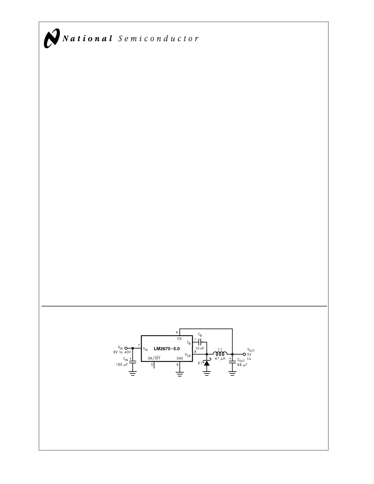
Typical Application
SIMPLE SWITCHER
®
is a registered trademark of National Semiconductor Corporation.
Windows
®
is a registered trademark of Microsoft Corporation.
DS012803-1
August 2000
LM2675
SIMPLE
SWITCHER
Power
Converter
High
Efficiency
1A
Step-Down
V
oltage
Regulator
© 2000 National Semiconductor Corporation
DS012803
www.national.com
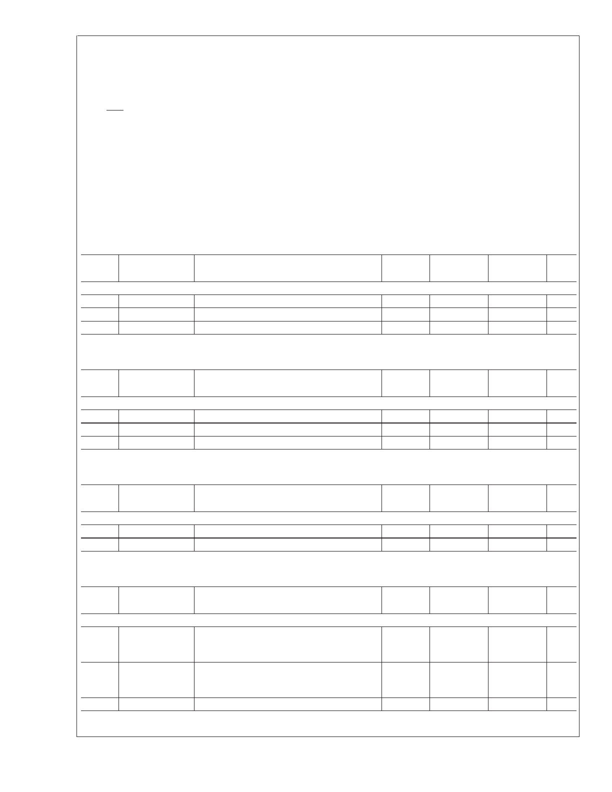
Absolute Maximum Ratings
(Note 1)
If Military/Aerospace specified devices are required,
please contact the National Semiconductor Sales Office/
Distributors for availability and specifications.
Supply Voltage
45V
ON/OFF Pin Voltage
−0.1V
≤
V
SH
≤
6V
Switch Voltage to Ground
−1V
Boost Pin Voltage
V
SW
+ 8V
Feedback Pin Voltage
−0.3V
≤
V
FB
≤
14V
ESD Susceptibility
Human Body Model (Note 2)
2 kV
Power Dissipation
Internally Limited
Storage Temperature Range
−65˚C to +150˚C
Lead Temperature
M Package
Vapor Phase (60s)
+215˚C
Infrared (15s)
+220˚C
N Package (Soldering, 10s)
+260˚C
Maximum Junction Temperature
+150˚C
Operating Ratings
Supply Voltage
6.5V to 40V
Junction Temperature Range
−40˚C
≤
T
J
≤
+125˚C
Electrical Characteristics
Specifications with standard type face are for T
J
= 25˚C, and those with bold
type face apply over full Operating Temperature Range.
LM2675-3.3
Symbol
Parameter
Conditions
Typical
Min
Max
Units
(Note 4)
(Note 5)
(Note 5)
SYSTEM PARAMETERS Test Circuit
Figure 2
(Note 3)
V
OUT
Output Voltage
V
IN
= 8V to 40V, I
LOAD
= 20 mA to 1A
3.3
3.251/3.201
3.350/3.399
V
V
OUT
Output Voltage
V
IN
= 6.5V to 40V, I
LOAD
= 20 mA to 500 mA
3.3
3.251/3.201
3.350/3.399
V
η
Efficiency
V
IN
= 12V, I
LOAD
= 1A
86
%
LM2675-5.0
Symbol
Parameter
Conditions
Typical
Min
Max
Units
(Note 4)
(Note 5)
(Note 5)
SYSTEM PARAMETERS Test Circuit
Figure 2
(Note 3)
V
OUT
Output Voltage
V
IN
= 8V to 40V, I
LOAD
= 20 mA to 1A
5.0
4.925/4.850
5.075/5.150
V
V
OUT
Output Voltage
V
IN
= 6.5V to 40V, I
LOAD
= 20 mA to 500 mA
5.0
4.925/4.850
5.075/5.150
V
η
Efficiency
V
IN
= 12V, I
LOAD
= 1A
90
%
LM2675-12
Symbol
Parameter
Conditions
Typical
Min
Max
Units
(Note 4)
(Note 5)
(Note 5)
SYSTEM PARAMETERS Test Circuit
Figure 2
(Note 3)
V
OUT
Output Voltage
V
IN
= 15V to 40V, I
LOAD
= 20 mA to 1A
12
11.82/11.64
12.18/12.36
V
η
Efficiency
V
IN
= 24V, I
LOAD
= 1A
94
%
LM2675-ADJ
Symbol
Parameter
Conditions
Typ
Min
Max
Units
(Note 4)
(Note 5)
(Note 5)
SYSTEM PARAMETERS Test Circuit
Figure 3
(Note 3)
V
FB
Feedback
Voltage
V
IN
= 8V to 40V, I
LOAD
= 20 mA to 1A
V
OUT
Programmed for 5V
(see Circuit of
Figure 3
)
1.210
1.192/1.174
1.228/1.246
V
V
FB
Feedback
Voltage
V
IN
= 6.5V to 40V, I
LOAD
= 20 mA to 500 mA
V
OUT
Programmed for 5V
(see Circuit of
Figure 3
)
1.210
1.192/1.174
1.228/1.246
V
η
Efficiency
V
IN
= 12V, I
LOAD
= 1A
90
%
LM2675
www.national.com
2
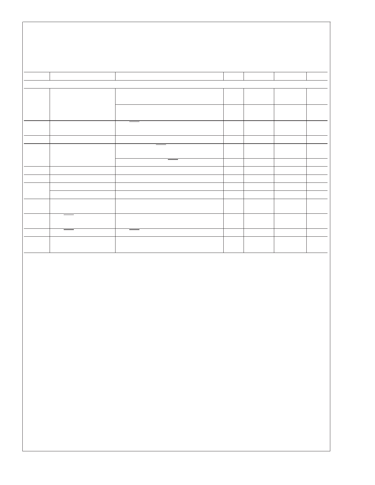
All Output Voltage Versions
Electrical Characteristics
Specifications with standard type face are for T
J
= 25˚C, and those with bold type face apply over full Operating Tempera-
ture Range. Unless otherwise specified, V
IN
= 12V for the 3.3V, 5V, and Adjustable versions and V
IN
= 24V for the 12V ver-
sion, and I
LOAD
= 100 mA.
Symbol
Parameters
Conditions
Typ
Min
Max
Units
DEVICE PARAMETERS
I
Q
Quiescent Current
V
FEEDBACK
= 8V
2.5
3.6
mA
For 3.3V, 5.0V, and ADJ Versions
V
FEEDBACK
= 15V
2.5
mA
For 12V Versions
I
STBY
Standby Quiescent
Current
ON/OFF Pin = 0V
50
100/150
µA
I
CL
Current Limit
1.55
1.25/1.2
2.1/2.2
A
I
L
Output Leakage Current
V
IN
= 40V, ON/OFF Pin = 0V
V
SWITCH
= 0V
1
25
µA
V
SWITCH
= −1V, ON/OFF Pin = 0V
6
15
mA
R
DS(ON)
Switch On-Resistance
I
SWITCH
= 1A
0.25
0.30/0.50
Ω
f
O
Oscillator Frequency
Measured at Switch Pin
260
225
275
kHz
D
Maximum Duty Cycle
95
%
Minimum Duty Cycle
0
%
I
BIAS
Feedback Bias
Current
V
FEEDBACK
= 1.3V
ADJ Version Only
85
nA
V
S/D
ON/OFF Pin
Voltage Thesholds
1.4
0.8
2.0
V
I
S/D
ON/OFF Pin Current
ON/OFF Pin = 0V
20
7
37
µA
θ
JA
Thermal Resistance
N Package, Junction to Ambient (Note 6)
95
˚C/W
M Package, Junction to Ambient (Note 6)
105
Note 1: Absolute Maximum Ratings indicate limits beyond which damage to the device may occur. Operating Ratings indicate conditions for which the device is in-
tended to be functional, but device parameter specifications may not be guaranteed under these conditions. For guaranteed specifications and test conditions, see
the Electrical Characteristics.
Note 2: The human body model is a 100 pF capacitor discharged through a 1.5 k
Ω
resistor into each pin.
Note 3: External components such as the catch diode, inductor, input and output capacitors, and voltage programming resistors can affect switching regulator per-
formance. When the LM2675 is used as shown in
Figures 2, 3 test circuits, system performance will be as specified by the system parameters section of the Electrical
Characteristics.
Note 4: Typical numbers are at 25˚C and represent the most likely norm.
Note 5: All limits guaranteed at room temperature (standard type face) and at temperature extremes (bold type face). All room temperature limits are 100% pro-
duction tested. All limits at temperature extremes are guaranteed via correlation using standard Statistical Quality Control (SQC) methods. All limits are used to cal-
culate Average Outgoing Quality Level (AOQL).
Note 6: Junction to ambient thermal resistance with approximately 1 square inch of printed circuit board copper surrounding the leads. Additional copper area will
lower thermal resistance further. See Application Information section in the application note accompanying this datasheet and the thermal model in
LM267X Made
Simple software (version 6.0).
LM2675
www.national.com
3
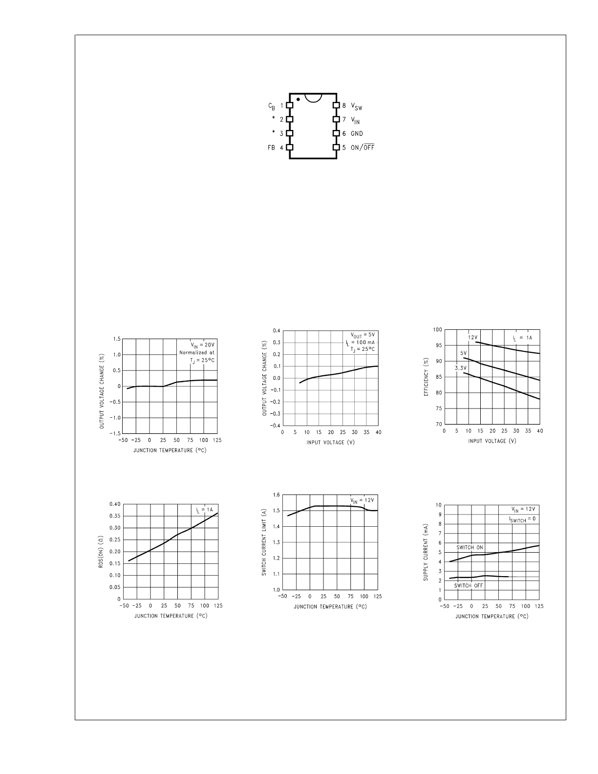
Connection Diagram and Ordering Information
Typical Performance Characteristics
8-Lead Package
Top View
DS012803-2
* No Connections
For Surface Mount Package
Order Number
LM2675M-3.3, LM2675M-5.0,
LM2675M-12 or LM2675M-ADJ
See NSC Package Number M08A
For DIP Package
Order Number
LM2675N-3.3, LM2675N-5.0,
LM2675N-12 or LM2675N-ADJ
See NSC Package Number N08E
Normalized
Output Voltage
DS012803-3
Line Regulation
DS012803-4
Efficiency
DS012803-5
Drain-to-Source
Resistance
DS012803-6
Switch Current Limit
DS012803-7
Operating
Quiescent Current
DS012803-8
LM2675
www.national.com
4
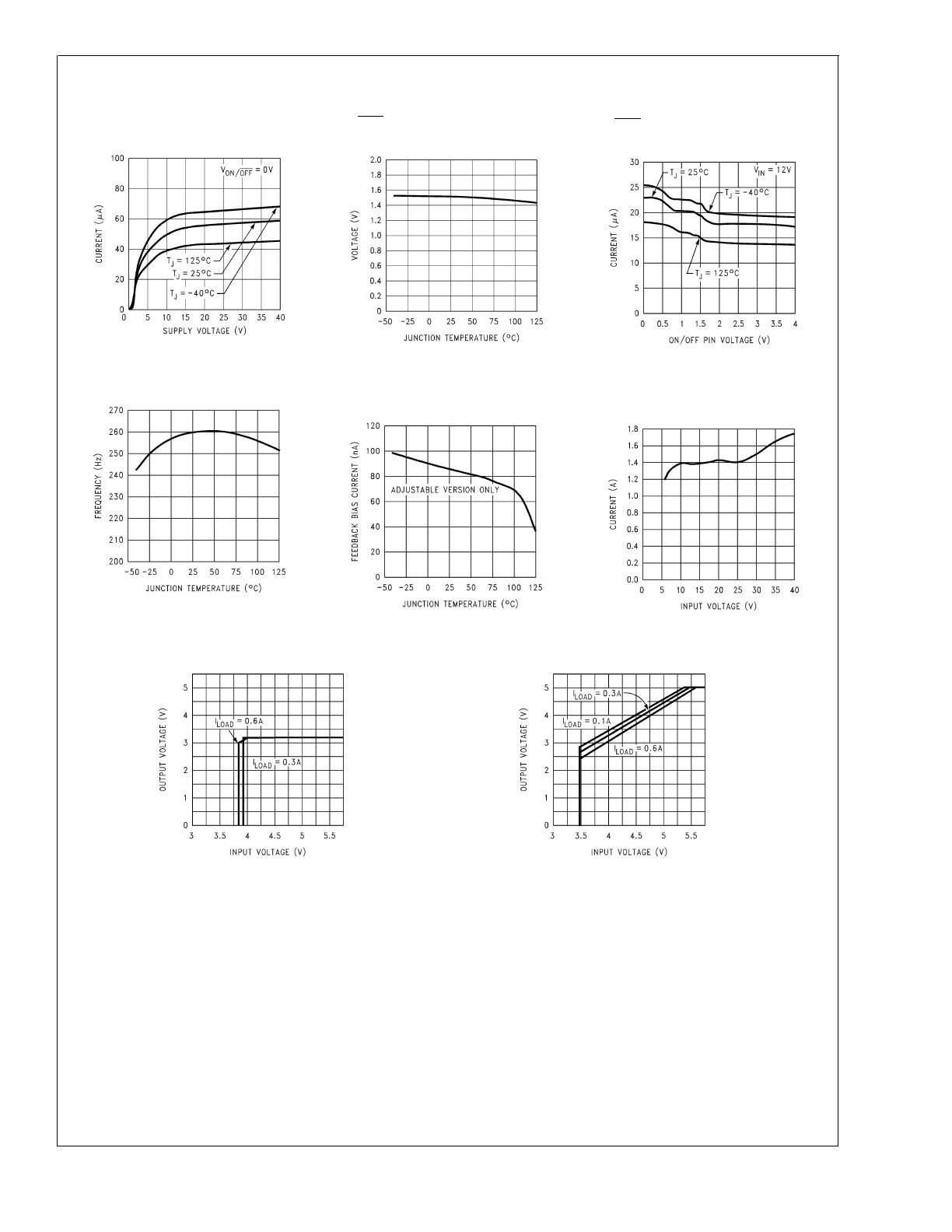
Typical Performance Characteristics
(Continued)
Standby
Quiescent Current
DS012803-9
ON/OFF Threshold
Voltage
DS012803-10
ON/OFF Pin
Current (Sourcing)
DS012803-11
Switching Frequency
DS012803-12
Feedback Pin
Bias Current
DS012803-13
Peak Switch Current
DS012803-14
Dropout Voltage — 3.3V Option
DS012803-15
Dropout Voltage — 5.0V Option
DS012803-16
LM2675
www.national.com
5
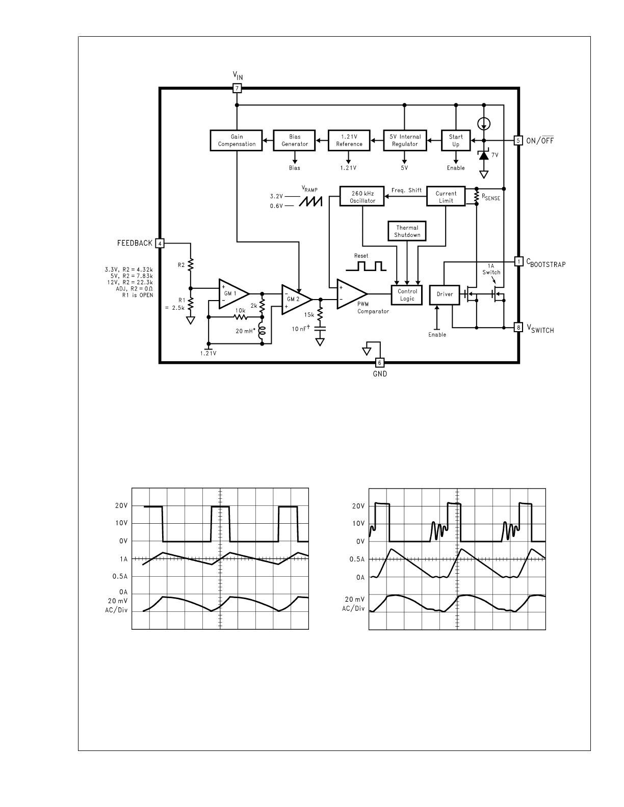
Block Diagram
Typical Performance Characteristics
(Circuit of
Figure 2
)
DS012803-17
* Active Inductor Patent Number 5,514,947
†
Active Capacitor Patent Number 5,382,918
FIGURE 1.
Continuous Mode Switching Waveforms
V
IN
= 20V, V
OUT
= 5V, I
LOAD
= 1A
L = 47 µH, C
OUT
= 68 µF, C
OUT
ESR = 50 m
Ω
DS012803-18
A: V
SW
Pin Voltage, 10 V/div.
B: Inductor Current, 0.5 A/div
C: Output Ripple Voltage, 20 mV/div AC-Coupled
Horizontal Time Base: 1 µs/div
Discontinuous Mode Switching Waveforms
V
IN
= 20V, V
OUT
= 5V, I
LOAD
= 300 mA
L = 15 µH, C
OUT
= 68 µF (2x), C
OUT
ESR = 25 m
Ω
DS012803-19
A: V
SW
Pin Voltage, 10 V/div.
B: Inductor Current, 0.5 A/div
C: Output Ripple Voltage, 20 mV/div AC-Coupled
Horizontal Time Base: 1 µs/div
LM2675
www.national.com
6
Typical Performance Characteristics
(Circuit of
Figure 2
) (Continued)
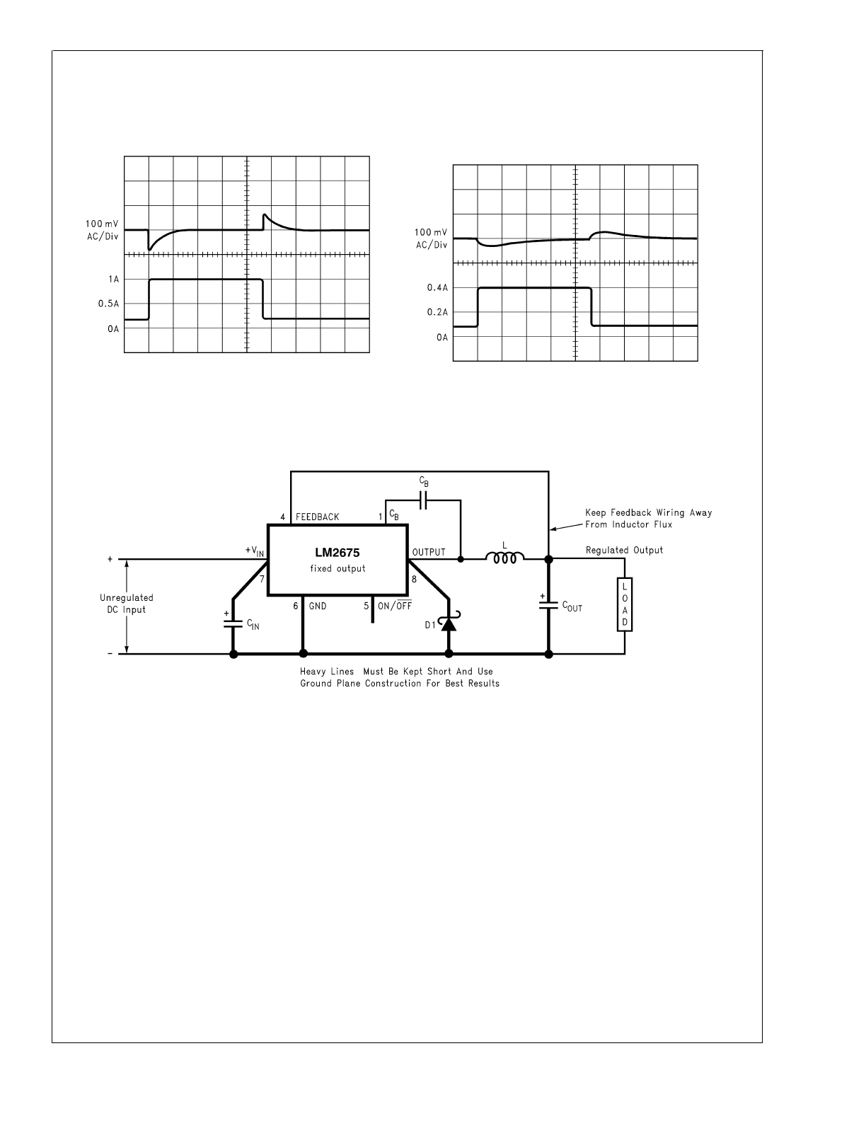
Test Circuit and Layout Guidelines
Load Transient Response for Continuous Mode
V
IN
= 20V, V
OUT
= 5V, I
LOAD
= 1A
L = 47 µH, C
OUT
= 68 µF, C
OUT
ESR = 50 m
Ω
DS012803-20
A: Output Voltage, 100 mV/div, AC-Coupled.
B: Load Current: 200 mA to 1A Load Pulse
Horizontal Time Base: 50 µs/div
Load Transient Response for Discontinuous Mode
V
IN
= 20V, V
OUT
= 5V,
L = 47 µH, C
OUT
= 68 µF, C
OUT
ESR = 50 m
Ω
DS012803-21
A: Output Voltage, 100 mV/div, AC-Coupled.
B: Load Current: 100 mA to 400 mA Load Pulse
Horizontal Time Base: 200 µs/div
DS012803-22
C
IN
- 22 µF, 50V Tantalum, Sprague “199D Series”
C
OUT
- 47 µF, 25V Tantalum, Sprague “595D Series”
D1 - 3.3A, 50V Schottky Rectifier, IR 30WQ05F
L1 - 68 µH Sumida #RCR110D-680L
C
B
- 0.01 µF, 50V Ceramic
FIGURE 2. Standard Test Circuits and Layout Guides
Fixed Output Voltage Versions
LM2675
www.national.com
7
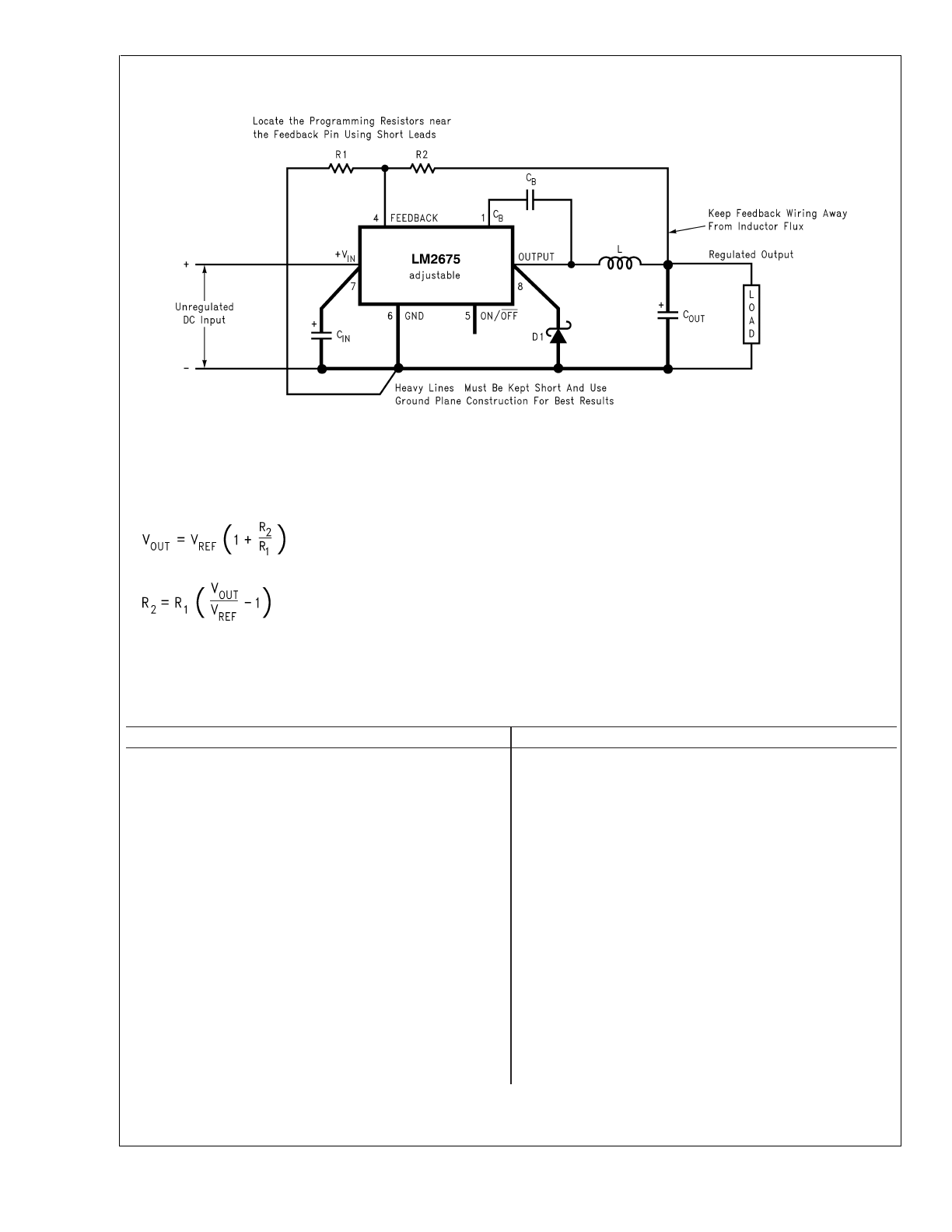
Test Circuit and Layout Guidelines
(Continued)
LM2675 Series Buck Regulator Design Procedure (Fixed Output)
PROCEDURE (Fixed Output Voltage Version)
EXAMPLE (Fixed Output Voltage Version)
To simplify the buck regulator design procedure, National
Semiconductor is making available computer design software
to be used with the
SIMPLE SWITCHER
line of switching
regulators. LM267X Made Simple version 6.0 is available on
Windows
®
3.1, NT, or 95 operating systems.
Given:
Given:
V
OUT
= Regulated Output Voltage (3.3V, 5V, or 12V)
V
OUT
= 5V
V
IN
(max) = Maximum DC Input Voltage
V
IN
(max) = 12V
I
LOAD
(max) = Maximum Load Current
I
LOAD
(max) = 1A
1. Inductor Selection (L1)
1. Inductor Selection (L1)
A. Select the correct inductor value selection guide from
Figure
4
,
Figure 5
or
Figure 6
(output voltages of 3.3V, 5V, or 12V
respectively). For all other voltages, see the design procedure
for the adjustable version.
A. Use the inductor selection guide for the 5V version shown
in
Figure 5
.
B. From the inductor value selection guide, identify the
inductance region intersected by the Maximum Input Voltage
line and the Maximum Load Current line. Each region is
identified by an inductance value and an inductor code (LXX).
B. From the inductor value selection guide shown in
Figure 5
,
the inductance region intersected by the 12V horizontal line
and the 1A vertical line is 33 µH, and the inductor code is L23.
DS012803-23
C
IN
- 22 µF, 50V Tantalum, Sprague “199D Series”
C
OUT
- 47 µF, 25V Tantalum, Sprague “595D Series”
D1 - 3.3A, 50V Schottky Rectifier, IR 30WQ05F
L1 - 68 µH Sumida #RCR110D-680L
R1 - 1.5 k
Ω
, 1%
C
B
- 0.01 µF, 50V Ceramic
For a 5V output, select R2 to be 4.75 k
Ω
, 1%
where V
REF
= 1.21V
Use a 1% resistor for best stability.
FIGURE 3. Standard Test Circuits and Layout Guides
Adjustable Output Voltage Versions
LM2675
www.national.com
8
LM2675 Series Buck Regulator Design Procedure (Fixed Output)
(Continued)
PROCEDURE (Fixed Output Voltage Version)
EXAMPLE (Fixed Output Voltage Version)
C. Select an appropriate inductor from the four manufacturer’s
part numbers listed in
Figure 8
. Each manufacturer makes a
different style of inductor to allow flexibility in meeting various
design requirements. Listed below are some of the
differentiating characteristics of each manufacturer’s inductors:
C. The inductance value required is 33 µH. From the table in
Figure 8
, go to the L23 line and choose an inductor part
number from any of the four manufacturers shown. (In most
instances, both through hole and surface mount inductors are
available.)
Schott:
ferrite EP core inductors; these have very low leakage
magnetic fields to reduce electro-magnetic interference (EMI)
and are the lowest power loss inductors
Renco:
ferrite stick core inductors; benefits are typically lowest
cost inductors and can withstand E
•
T and transient peak
currents above rated value. Be aware that these inductors
have an external magnetic field which may generate more EMI
than other types of inductors.
Pulse:
powered iron toroid core inductors; these can also be
low cost and can withstand larger than normal E
•
T and
transient peak currents. Toroid inductors have low EMI.
Coilcraft:
ferrite drum core inductors; these are the smallest
physical size inductors, available only as SMT components. Be
aware that these inductors also generate EMI — but less than
stick inductors.
Complete specifications for these inductors are available from
the respective manufacturers. A table listing the manufacturers’
phone numbers is located in
Figure 9
.
2. Output Capacitor Selection (C
OUT
)
2. Output Capacitor Selection (C
OUT
)
A. Select an output capacitor from the output capacitor table in
Figure 10
. Using the output voltage and the inductance value
found in the inductor selection guide, step 1, locate the
appropriate capacitor value and voltage rating.
A. Use the 5.0V section in the output capacitor table in
Figure
10
. Choose a capacitor value and voltage rating from the line
that contains the inductance value of 33 µH. The capacitance
and voltage rating values corresponding to the 33 µH inductor
are the:
The capacitor list contains through-hole electrolytic capacitors
from four different capacitor manufacturers and surface mount
tantalum capacitors from two different capacitor manufacturers.
It is recommended that both the manufacturers and the
manufacturer’s series that are listed in the table be used. A
table listing the manufacturers’ phone numbers is located in
Figure 11
.
Surface Mount:
68 µF/10V
Sprague 594D Series.
100 µF/10V
AVX TPS Series.
Through Hole:
68 µF/10V
Sanyo OS-CON SA Series.
220 µF/35V
Sanyo MV-GX Series.
220 µF/35V
Nichicon PL Series.
220 µF/35V
Panasonic HFQ Series.
3. Catch Diode Selection (D1)
A. In normal operation, the average current of the catch diode
is the load current times the catch diode duty cycle, 1-D (D is
the switch duty cycle, which is approximately the output
voltage divided by the input voltage). The largest value of the
catch diode average current occurs at the maximum load
current and maximum input voltage (minimum D). For normal
operation, the catch diode current rating must be at least 1.3
times greater than its maximum average current. However, if
the power supply design must withstand a continuous output
short, the diode should have a current rating equal to the
maximum current limit of the LM2675. The most stressful
condition for this diode is a shorted output condition.
3. Catch Diode Selection (D1)
A. Refer to the table shown in
Figure 12
. In this example, a
1A, 20V Schottky diode will provide the best performance. If
the circuit must withstand a continuous shorted output, a
higher current Schottky diode is recommended.
B. The reverse voltage rating of the diode should be at least
1.25 times the maximum input voltage.
C. Because of their fast switching speed and low forward
voltage drop, Schottky diodes provide the best performance
and efficiency. This Schottky diode must be located close to
the LM2675 using short leads and short printed circuit traces.
LM2675
www.national.com
9
LM2675 Series Buck Regulator Design Procedure (Fixed Output)
(Continued)
PROCEDURE (Fixed Output Voltage Version)
EXAMPLE (Fixed Output Voltage Version)
4. Input Capacitor (C
IN
)
4. Input Capacitor (C
IN
)
A low ESR aluminum or tantalum bypass capacitor is needed
between the input pin and ground to prevent large voltage
transients from appearing at the input. This capacitor should
be located close to the IC using short leads. In addition, the
RMS current rating of the input capacitor should be selected to
be at least
1
⁄
2
the DC load current. The capacitor manufacturer
data sheet must be checked to assure that this current rating
is not exceeded. The curves shown in
Figure 14
show typical
RMS current ratings for several different aluminum electrolytic
capacitor values. A parallel connection of two or more
capacitors may be required to increase the total minimum RMS
current rating to suit the application requirements.
For an aluminum electrolytic capacitor, the voltage rating
should be at least 1.25 times the maximum input voltage.
Caution must be exercised if solid tantalum capacitors are
used. The tantalum capacitor voltage rating should be twice
the maximum input voltage. The tables in
Figure 15
show the
recommended application voltage for AVX TPS and Sprague
594D tantalum capacitors. It is also recommended that they be
surge current tested by the manufacturer. The TPS series
available from AVX, and the 593D and 594D series from
Sprague are all surge current tested. Another approach to
minimize the surge current stresses on the input capacitor is to
add a small inductor in series with the input supply line.
Use caution when using ceramic capacitors for input
bypassing, because it may cause severe ringing at the V
IN
pin.
The important parameters for the input capacitor are the input
voltage rating and the RMS current rating. With a maximum
input voltage of 12V, an aluminum electrolytic capacitor with a
voltage rating greater than 15V (1.25 x V
IN
) would be needed.
The next higher capacitor voltage rating is 16V.
The RMS current rating requirement for the input capacitor in a
buck regulator is approximately
1
⁄
2
the DC load current. In this
example, with a 1A load, a capacitor with a RMS current rating
of at least 500 mA is needed. The curves shown in
Figure 14
can be used to select an appropriate input capacitor. From the
curves, locate the 16V line and note which capacitor values
have RMS current ratings greater than 500 mA.
For a through hole design, a 330 µF/16V electrolytic capacitor
(Panasonic HFQ series, Nichicon PL, Sanyo MV-GX series or
equivalent) would be adequate. Other types or other
manufacturers’ capacitors can be used provided the RMS
ripple current ratings are adequate. Additionally, for a complete
surface mount design, electrolytic capacitors such as the
Sanyo CV-C or CV-BS and the Nichicon WF or UR and the
NIC Components NACZ series could be considered.
For surface mount designs, solid tantalum capacitors can be
used, but caution must be exercised with regard to the
capacitor surge current rating and voltage rating. In this
example, checking
Figure 15
, and the Sprague 594D series
datasheet, a Sprague 594D 15 µF, 25V capacitor is adequate.
5. Boost Capacitor (C
B
)
5. Boost Capacitor (C
B
)
This capacitor develops the necessary voltage to turn the
switch gate on fully. All applications should use a 0.01 µF, 50V
ceramic capacitor.
For this application, and all applications, use a 0.01 µF, 50V
ceramic capacitor.
LM2675
www.national.com
10
LM2675 Series Buck Regulator Design Procedure (Fixed Output)
(Continued)
INDUCTOR VALUE SELECTION GUIDES (For Continuous Mode Operation)
DS012803-26
FIGURE 4. LM2675-3.3
DS012803-27
FIGURE 5. LM2675-5.0
DS012803-28
FIGURE 6. LM2675-12
DS012803-29
FIGURE 7. LM2675-ADJ
LM2675
www.national.com
11
LM2675 Series Buck Regulator Design Procedure (Fixed Output)
(Continued)
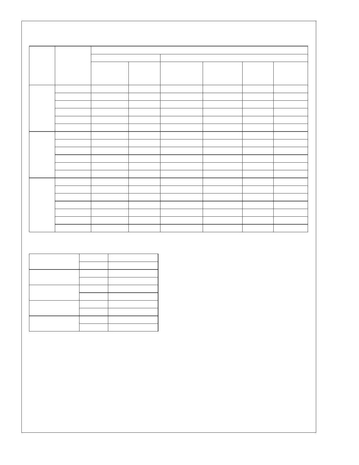
Ind.
Ref.
Desg.
Induc-
tance
(µH)
Current
(A)
Schott
Renco
Pulse Engineering
Coilcraft
Through
Surface
Through
Surface
Through
Surface
Surface
Hole
Mount
Hole
Mount
Hole
Mount
Mount
L4
68
0.32
67143940
67144310 RL-1284-68-43
RL1500-68
PE-53804 PE-53804-S DO1608-683
L5
47
0.37
67148310
67148420 RL-1284-47-43
RL1500-47
PE-53805 PE-53805-S DO1608-473
L6
33
0.44
67148320
67148430 RL-1284-33-43
RL1500-33
PE-53806 PE-53806-S DO1608-333
L7
22
0.52
67148330
67148440 RL-1284-22-43
RL1500-22
PE-53807 PE-53807-S DO1608-223
L9
220
0.32
67143960
67144330
RL-5470-3
RL1500-220
PE-53809 PE-53809-S DO3308-224
L10
150
0.39
67143970
67144340
RL-5470-4
RL1500-150
PE-53810 PE-53810-S DO3308-154
L11
100
0.48
67143980
67144350
RL-5470-5
RL1500-100
PE-53811 PE-53811-S DO3308-104
L12
68
0.58
67143990
67144360
RL-5470-6
RL1500-68
PE-53812 PE-53812-S DO3308-683
L13
47
0.70
67144000
67144380
RL-5470-7
RL1500-47
PE-53813 PE-53813-S DO3308-473
L14
33
0.83
67148340
67148450 RL-1284-33-43
RL1500-33
PE-53814 PE-53814-S DO3308-333
L15
22
0.99
67148350
67148460 RL-1284-22-43
RL1500-22
PE-53815 PE-53815-S DO3308-223
L18
220
0.55
67144040
67144420
RL-5471-2
RL1500-220
PE-53818 PE-53818-S DO3316-224
L19
150
0.66
67144050
67144430
RL-5471-3
RL1500-150
PE-53819 PE-53819-S DO3316-154
L20
100
0.82
67144060
67144440
RL-5471-4
RL1500-100
PE-53820 PE-53820-S DO3316-104
L21
68
0.99
67144070
67144450
RL-5471-5
RL1500-68
PE-53821 PE-53821-S DO3316-683
L22
47
1.17
67144080
67144460
RL-5471-6
—
PE-53822 PE-53822-S DO3316-473
L23
33
1.40
67144090
67144470
RL-5471-7
—
PE-53823 PE-53823-S DO3316-333
L24
22
1.70
67148370
67148480 RL-1283-22-43
—
PE-53824 PE-53824-S DO3316-223
L27
220
1.00
67144110
67144490
RL-5471-2
—
PE-53827 PE-53827-S
DO5022P-224
L28
150
1.20
67144120
67144500
RL-5471-3
—
PE-53828 PE-53828-S
DO5022P-154
L29
100
1.47
67144130
67144510
RL-5471-4
—
PE-53829 PE-53829-S
DO5022P-104
L30
68
1.78
67144140
67144520
RL-5471-5
—
PE-53830 PE-53830-S
DO5022P-683
FIGURE 8. Inductor Manufacturers’ Part Numbers
Coilcraft Inc.
Phone
(800) 322-2645
FAX
(708) 639-1469
Coilcraft Inc., Europe
Phone
+44 1236 730 595
FAX
+44 1236 730 627
Pulse Engineering Inc.
Phone
(619) 674-8100
FAX
(619) 674-8262
Pulse Engineering Inc.,
Phone
+353 93 24 107
Europe
FAX
+353 93 24 459
Renco Electronics Inc.
Phone
(800) 645-5828
FAX
(516) 586-5562
Schott Corp.
Phone
(612) 475-1173
FAX
(612) 475-1786
FIGURE 9. Inductor Manufacturers’ Phone Numbers
LM2675
www.national.com
12
LM2675 Series Buck Regulator Design Procedure (Fixed Output)
(Continued)
Output
Voltage
(V)
Inductance
(µH)
Output Capacitor
Surface Mount
Through Hole
Sprague
AVX TPS
Sanyo OS-CON
Sanyo MV-GX
Nichicon
Panasonic
594D Series
Series
SA Series
Series
PL Series
HFQ Series
(µF/V)
(µF/V)
(µF/V)
(µF/V)
(µF/V)
(µF/V)
3.3
22
120/6.3
100/10
100/10
330/35
330/35
330/35
33
120/6.3
100/10
68/10
220/35
220/35
220/35
47
68/10
100/10
68/10
150/35
150/35
150/35
68
120/6.3
100/10
100/10
120/35
120/35
120/35
100
120/6.3
100/10
100/10
120/35
120/35
120/35
150
120/6.3
100/10
100/10
120/35
120/35
120/35
5.0
22
100/16
100/10
100/10
330/35
330/35
330/35
33
68/10
10010
68/10
220/35
220/35
220/35
47
68/10
100/10
68/10
150/35
150/35
150/35
68
100/16
100/10
100/10
120/35
120/35
120/35
100
100/16
100/10
100/10
120/35
120/35
120/35
150
100/16
100/10
100/10
120/35
120/35
120/35
12
22
120/20
(2x) 68/20
68/20
330/35
330/35
330/35
33
68/25
68/20
68/20
220/35
220/35
220/35
47
47/20
68/20
47/20
150/35
150/35
150/35
68
47/20
68/20
47/20
120/35
120/35
120/35
100
47/20
68/20
47/20
120/35
120/35
120/35
150
47/20
68/20
47/20
120/35
120/35
120/35
220
47/20
68/20
47/20
120/35
120/35
120/35
FIGURE 10. Output Capacitor Table
Nichicon Corp.
Phone
(847) 843-7500
FAX
(847) 843-2798
Panasonic
Phone
(714) 373-7857
FAX
(714) 373-7102
AVX Corp.
Phone
(803) 448-9411
FAX
(803) 448-1943
Sprague/Vishay
Phone
(207) 324-4140
FAX
(207) 324-7223
Sanyo Corp.
Phone
(619) 661-6322
FAX
(619) 661-1055
FIGURE 11. Capacitor Manufacturers’ Phone Numbers
LM2675
www.national.com
13
LM2675 Series Buck Regulator Design Procedure (Fixed Output)
(Continued)
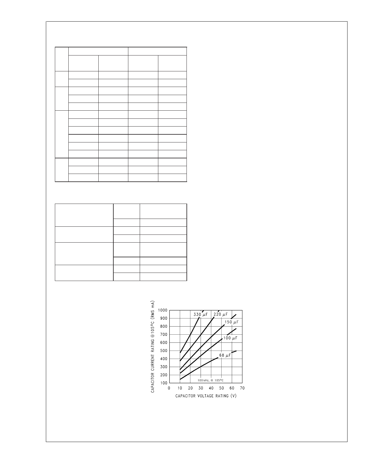
V
R
1A Diodes
3A Diodes
Surface
Through
Surface
Through
Mount
Hole
Mount
Hole
20V
SK12
1N5817
SK32
1N5820
B120
SR102
SR302
30V
SK13
1N5818
SK33
1N5821
B130
11DQ03
30WQ03F
31DQ03
MBRS130
SR103
40V
SK14
1N5819
SK34
1N5822
B140
11DQ04
30BQ040
MBR340
MBRS140
SR104
30WQ04F
31DQ04
10BQ040
MBRS340
SR304
10MQ040
MBRD340
15MQ040
50V
SK15
MBR150
SK35
MBR350
B150
11DQ05
30WQ05F
31DQ05
10BQ050
SR105
SR305
FIGURE 12. Schottky Diode Selection Table
International Rectifier
Corp.
Phone
(310) 322-3331
FAX
(310) 322-3332
Motorola, Inc.
Phone
(800) 521-6274
FAX
(602) 244-6609
General Instruments
Corp.
Phone
(516) 847-3000
FAX
(516) 847-3236
Diodes, Inc.
Phone
(805) 446-4800
FAX
(805) 446-4850
FIGURE 13. Diode Manufacturers’ Phone Numbers
DS012803-30
FIGURE 14. RMS Current Ratings for Low ESR Electrolytic Capacitors (Typical)
LM2675
www.national.com
14
LM2675 Series Buck Regulator Design Procedure (Fixed Output)
(Continued)
LM2675 Series Buck Regulator Design Procedure (Adjustable Output)
PROCEDURE (Adjustable Output Voltage Version)
EXAMPLE (Adjustable Output Voltage Version)
To simplify the buck regulator design procedure, National
Semiconductor is making available computer design software
to be used with the
SIMPLE SWITCHER
line of switching
regulators. LM267X Made Simple version 6.0 is available for
use on
Windows
3.1, NT, or 95 operating systems.
Given:
Given:
V
OUT
= Regulated Output Voltage
V
OUT
= 20V
V
IN
(max) = Maximum Input Voltage
V
IN
(max) = 28V
I
LOAD
(max) = Maximum Load Current
I
LOAD
(max) = 1A
F = Switching Frequency
(Fixed at a nominal 260 kHz).
F = Switching Frequency
(Fixed at a nominal 260 kHz).
1. Programming Output Voltage (Selecting R
1
and R
2
, as
shown in
Figure 3
)
1. Programming Output Voltage (Selecting R
1
and R
2
, as
shown in
Figure 3
)
Use the following formula to select the appropriate resistor
values.
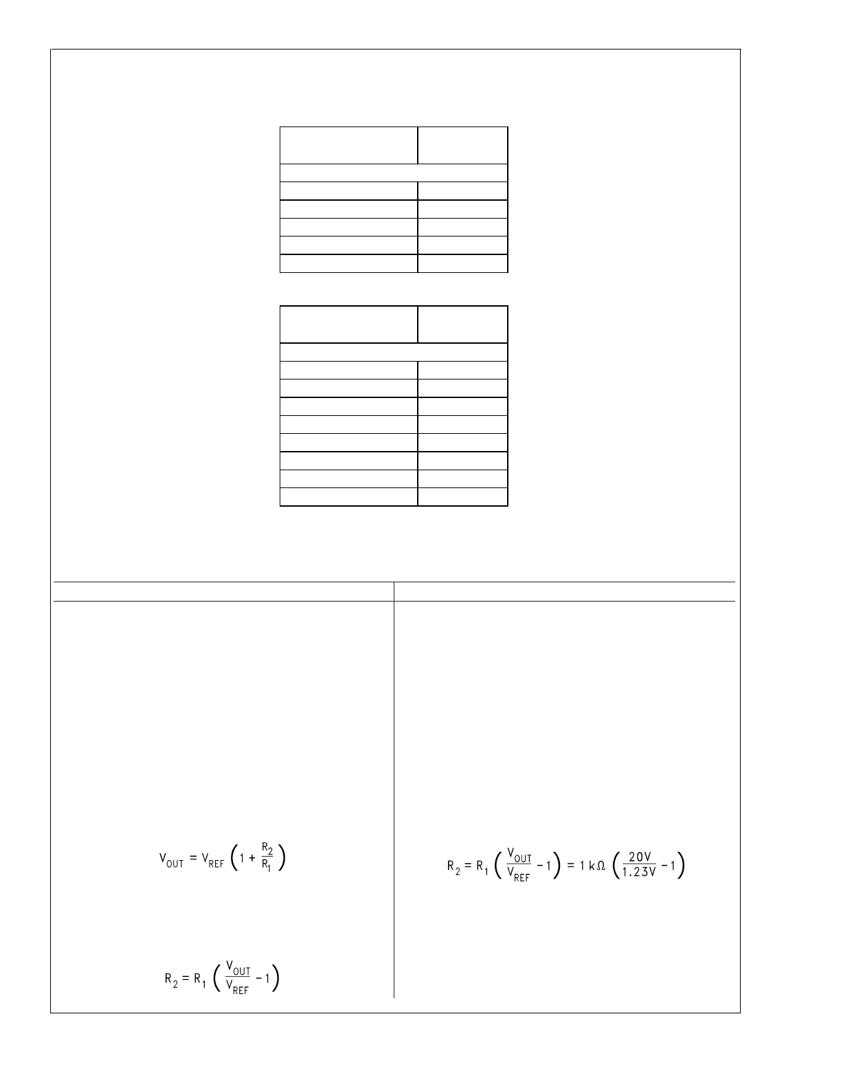
Select R
1
to be 1 k
Ω
, 1%. Solve for R
2
.
where V
REF
= 1.21V
Select a value for R
1
between 240
Ω
and 1.5 k
Ω
. The lower
resistor values minimize noise pickup in the sensitive feedback
pin. (For the lowest temperature coefficient and the best
stability with time, use 1% metal film resistors.)
R
2
= 1k (16.53 − 1) = 15.53 k
Ω
, closest 1% value is 15.4 k
Ω
.
R
2
= 15.4 k
Ω
.
AVX TPS
Recommended
Voltage
Application Voltage
Rating
+85˚C Rating
3.3
6.3
5
10
10
20
12
25
15
35
Sprague 594D
Recommended
Voltage
Application Voltage
Rating
+85˚C Rating
2.5
4
3.3
6.3
5
10
8
16
12
20
18
25
24
35
29
50
FIGURE 15. Recommended Application Voltage for AVX TPS and
Sprague 594D Tantalum Chip Capacitors Derated for 85˚C.
LM2675
www.national.com
15
LM2675 Series Buck Regulator Design Procedure (Adjustable Output)
(Continued)
PROCEDURE (Adjustable Output Voltage Version)
EXAMPLE (Adjustable Output Voltage Version)
2. Inductor Selection (L1)
2. Inductor Selection (L1)
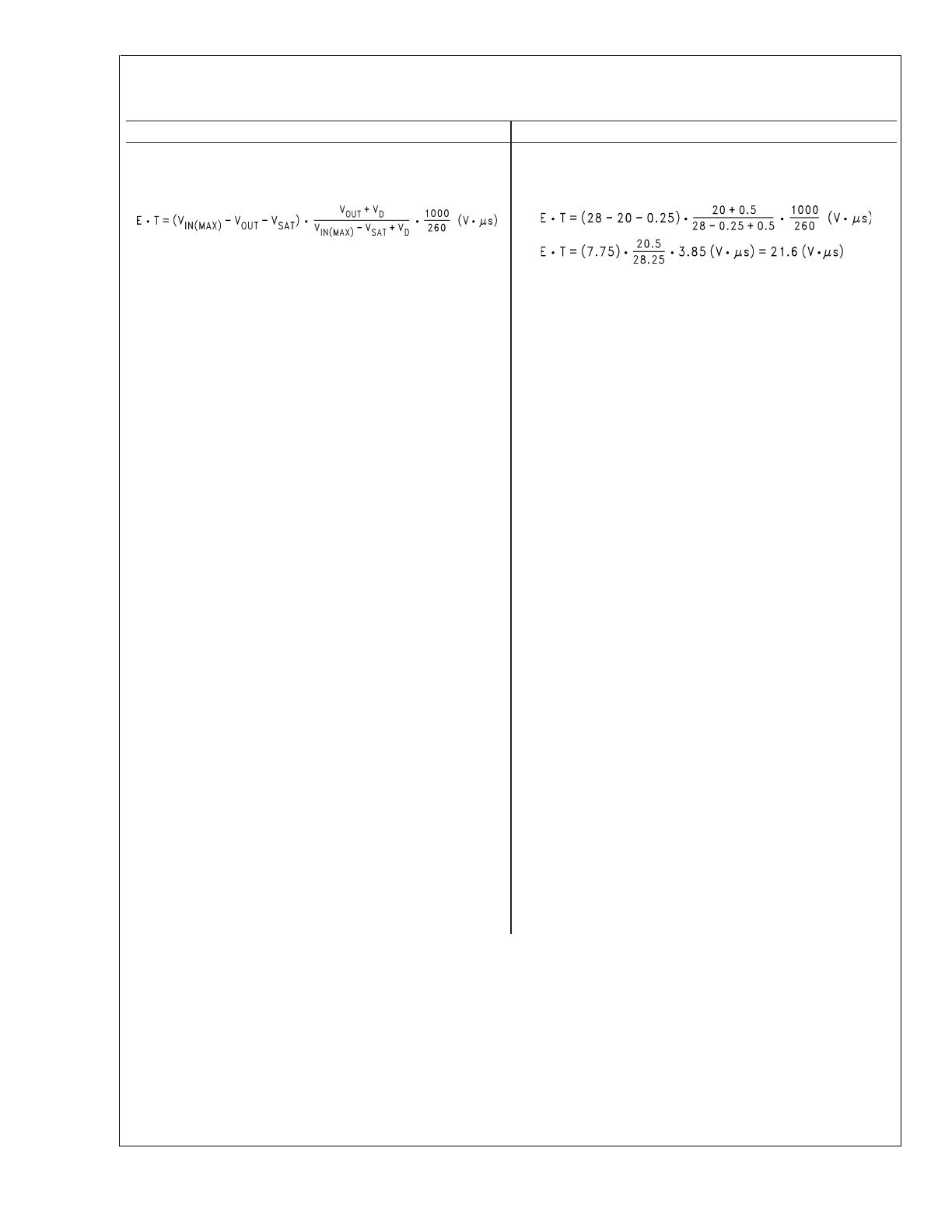
A. Calculate the inductor Volt
•
microsecond constant E
•
T (V
•
µs), from the following formula:
A. Calculate the inductor Volt
•
microsecond constant (E
•
T),
where V
SAT
= internal switch saturation voltage = 0.25V and
V
D
= diode forward voltage drop = 0.5V
B. Use the E
•
T value from the previous formula and match it
with the E
•
T number on the vertical axis of the Inductor
Value Selection Guide shown in
Figure 7
.
B. E
•
T = 21.6 (V
•
µs)
C. On the horizontal axis, select the maximum load current.
C. I
LOAD
(max) = 1A
D. Identify the inductance region intersected by the E
•
T value
and the Maximum Load Current value. Each region is identified
by an inductance value and an inductor code (LXX).
D. From the inductor value selection guide shown in
Figure 7
,
the inductance region intersected by the 21.6 (V
•
µs)
horizontal line and the 1A vertical line is 68 µH, and the
inductor code is L30.
E. Select an appropriate inductor from the four manufacturer’s
part numbers listed in
Figure 8
. For information on the different
types of inductors, see the inductor selection in the fixed
output voltage design procedure.
E. From the table in
Figure 8
, locate line L30, and select an
inductor part number from the list of manufacturers part
numbers.
3. Output Capacitor Selection (C
OUT
)
3. Output Capacitor SeIection (C
OUT
)
A. Select an output capacitor from the capacitor code selection
guide in
Figure 16
. Using the inductance value found in the
inductor selection guide, step 1, locate the appropriate
capacitor code corresponding to the desired output voltage.
A. Use the appropriate row of the capacitor code selection
guide, in
Figure 16
. For this example, use the 15–20V row.
The capacitor code corresponding to an inductance of 68 µH is
C20.
B. Select an appropriate capacitor value and voltage rating,
using the capacitor code, from the output capacitor selection
table in
Figure 17
. There are two solid tantalum (surface
mount) capacitor manufacturers and four electrolytic (through
hole) capacitor manufacturers to choose from. It is
recommended that both the manufacturers and the
manufacturer’s series that are listed in the table be used. A
table listing the manufacturers’ phone numbers is located in
Figure 11
.
B. From the output capacitor selection table in
Figure 17
,
choose a capacitor value (and voltage rating) that intersects
the capacitor code(s) selected in section A, C20.
The capacitance and voltage rating values corresponding to
the capacitor code C20 are the:
Surface Mount:
33 µF/25V
Sprague 594D Series.
33 µF/25V
AVX TPS Series.
Through Hole:
33 µF/25V
Sanyo OS-CON SC Series.
120 µF/35V
Sanyo MV-GX Series.
120 µF/35V
Nichicon PL Series.
120 µF/35V
Panasonic HFQ Series.
Other manufacturers or other types of capacitors may also be
used, provided the capacitor specifications (especially the 100
kHz ESR) closely match the characteristics of the capacitors
listed in the output capacitor table. Refer to the capacitor
manufacturers’ data sheet for this information.
LM2675
www.national.com
16
LM2675 Series Buck Regulator Design Procedure (Adjustable Output)
(Continued)
PROCEDURE (Adjustable Output Voltage Version)
EXAMPLE (Adjustable Output Voltage Version)
4. Catch Diode Selection (D1)
A. In normal operation, the average current of the catch diode
is the load current times the catch diode duty cycle, 1-D (D is
the switch duty cycle, which is approximately V
OUT
/V
IN
). The
largest value of the catch diode average current occurs at the
maximum input voltage (minimum D). For normal operation,
the catch diode current rating must be at least 1.3 times
greater than its maximum average current. However, if the
power supply design must withstand a continuous output short,
the diode should have a current rating greater than the
maximum current limit of the LM2675. The most stressful
condition for this diode is a shorted output condition.
4. Catch Diode Selection (D1)
A. Refer to the table shown in
Figure 12
. Schottky diodes
provide the best performance, and in this example a 1A, 40V
Schottky diode would be a good choice. If the circuit must
withstand a continuous shorted output, a higher current (at
least 2.2A) Schottky diode is recommended.
B. The reverse voltage rating of the diode should be at least
1.25 times the maximum input voltage.
C. Because of their fast switching speed and low forward
voltage drop, Schottky diodes provide the best performance
and efficiency. The Schottky diode must be located close to
the LM2675 using short leads and short printed circuit traces.
5. Input Capacitor (C
IN
)
A low ESR aluminum or tantalum bypass capacitor is needed
between the input pin and ground to prevent large voltage
transients from appearing at the input. This capacitor should
be located close to the IC using short leads. In addition, the
RMS current rating of the input capacitor should be selected to
be at least
1
⁄
2
the DC load current. The capacitor manufacturer
data sheet must be checked to assure that this current rating
is not exceeded. The curves shown in
Figure 14
show typical
RMS current ratings for several different aluminum electrolytic
capacitor values. A parallel connection of two or more
capacitors may be required to increase the total minimum RMS
current rating to suit the application requirements.
For an aluminum electrolytic capacitor, the voltage rating
should be at least 1.25 times the maximum input voltage.
Caution must be exercised if solid tantalum capacitors are
used. The tantalum capacitor voltage rating should be twice
the maximum input voltage. The tables in
Figure 15
show the
recommended application voltage for AVX TPS and Sprague
594D tantalum capacitors. It is also recommended that they be
surge current tested by the manufacturer. The TPS series
available from AVX, and the 593D and 594D series from
Sprague are all surge current tested. Another approach to
minimize the surge current stresses on the input capacitor is to
add a small inductor in series with the input supply line.
Use caution when using ceramic capacitors for input
bypassing, because it may cause severe ringing at the V
IN
pin.
5. Input Capacitor (C
IN
)
The important parameters for the input capacitor are the input
voltage rating and the RMS current rating. With a maximum
input voltage of 28V, an aluminum electrolytic capacitor with a
voltage rating of at least 35V (1.25 x V
IN
) would be needed.
The RMS current rating requirement for the input capacitor in a
buck regulator is approximately
1
⁄
2
the DC load current. In this
example, with a 1A load, a capacitor with a RMS current rating
of at least 500 mA is needed. The curves shown in
Figure 14
can be used to select an appropriate input capacitor. From the
curves, locate the 35V line and note which capacitor values
have RMS current ratings greater than 500 mA.
For a through hole design, a 330 µF/35V electrolytic capacitor
(Panasonic HFQ series, Nichicon PL, Sanyo MV-GX series or
equivalent) would be adequate. Other types or other
manufacturers’ capacitors can be used provided the RMS
ripple current ratings are adequate. Additionally, for a complete
surface mount design, electrolytic capacitors such as the
Sanyo CV-C or CV-BS, and the Nichicon WF or UR and the
NIC Components NACZ series could be considered.
For surface mount designs, solid tantalum capacitors can be
used, but caution must be exercised with regard to the
capacitor surge current rating and voltage rating. In this
example, checking
Figure 15
, and the Sprague 594D series
datasheet, a Sprague 594D 15 µF, 50V capacitor is adequate.
6. Boost Capacitor (C
B
)
6. Boost Capacitor (C
B
)
This capacitor develops the necessary voltage to turn the
switch gate on fully. All applications should use a 0.01 µF, 50V
ceramic capacitor.
For this application, and all applications, use a 0.01 µF, 50V
ceramic capacitor.
LM2675
www.national.com
17
LM2675 Series Buck Regulator Design Procedure (Adjustable Output)
(Continued)
Case
Style (Note 7)
Output
Voltage (V)
Inductance (µH)
22
33
47
68
100
150
220
SM and TH
1.21–2.50
—
—
—
—
C1
C2
C3
SM and TH
2.50–3.75
—
—
—
C1
C2
C3
C3
SM and TH
3.75–5.0
—
—
C4
C5
C6
C6
C6
SM and TH
5.0–6.25
—
C4
C7
C6
C6
C6
C6
SM and TH
6.25–7.5
C8
C4
C7
C6
C6
C6
C6
SM and TH
7.5–10.0
C9
C10
C11
C12
C13
C13
C13
SM and TH
10.0–12.5
C14
C11
C12
C12
C13
C13
C13
SM and TH
12.5–15.0
C15
C16
C17
C17
C17
C17
C17
SM and TH
15.0–20.0
C18
C19
C20
C20
C20
C20
C20
SM and TH
20.0–30.0
C21
C22
C22
C22
C22
C22
C22
TH
30.0–37.0
C23
C24
C24
C25
C25
C25
C25
Note 7: SM - Surface Mount,
TH - Through Hole
FIGURE 16. Capacitor Code Selection Guide
LM2675
www.national.com
18
LM2675 Series Buck Regulator Design Procedure (Adjustable Output)
(Continued)
Output Capacitor
Cap.
Ref.
Desg.
#
Surface Mount
Through Hole
Sprague
AVX TPS
Sanyo OS-CON
Sanyo MV-GX
Nichicon
Panasonic
594D Series
Series
SA Series
Series
PL Series
HFQ Series
(µF/V)
(µF/V)
(µF/V)
(µF/V)
(µF/V)
(µF/V)
C1
120/6.3
100/10
100/10
220/35
220/35
220/35
C2
120/6.3
100/10
100/10
150/35
150/35
150/35
C3
120/6.3
100/10
100/35
120/35
120/35
120/35
C4
68/10
100/10
68/10
220/35
220/35
220/35
C5
100/16
100/10
100/10
150/35
150/35
150/35
C6
100/16
100/10
100/10
120/35
120/35
120/35
C7
68/10
100/10
68/10
150/35
150/35
150/35
C8
100/16
100/10
100/10
330/35
330/35
330/35
C9
100/16
100/16
100/16
330/35
330/35
330/35
C10
100/16
100/16
68/16
220/35
220/35
220/35
C11
100/16
100/16
68/16
150/35
150/35
150/35
C12
100/16
100/16
68/16
120/35
120/35
120/35
C13
100/16
100/16
100/16
120/35
120/35
120/35
C14
100/16
100/16
100/16
220/35
220/35
220/35
C15
47/20
68/20
47/20
220/35
220/35
220/35
C16
47/20
68/20
47/20
150/35
150/35
150/35
C17
47/20
68/20
47/20
120/35
120/35
120/35
C18
68/25
(2x) 33/25
47/25 (Note 8)
220/35
220/35
220/35
C19
33/25
33/25
33/25 (Note 8)
150/35
150/35
150/35
C20
33/25
33/25
33/25 (Note 8)
120/35
120/35
120/35
C21
33/35
(2x) 22/25
(Note 9)
150/35
150/35
150/35
C22
33/35
22/35
(Note 9)
120/35
120/35
120/35
C23
(Note 9)
(Note 9)
(Note 9)
220/50
100/50
120/50
C24
(Note 9)
(Note 9)
(Note 9)
150/50
100/50
120/50
C25
(Note 9)
(Note 9)
(Note 9)
150/50
82/50
82/50
Note 8: The SC series of Os-Con capacitors (others are SA series)
Note 9: The voltage ratings of the surface mount tantalum chip and Os-Con capacitors are too low to work at these voltages.
FIGURE 17. Output Capacitor Selection Table
LM2675
www.national.com
19
Application Information
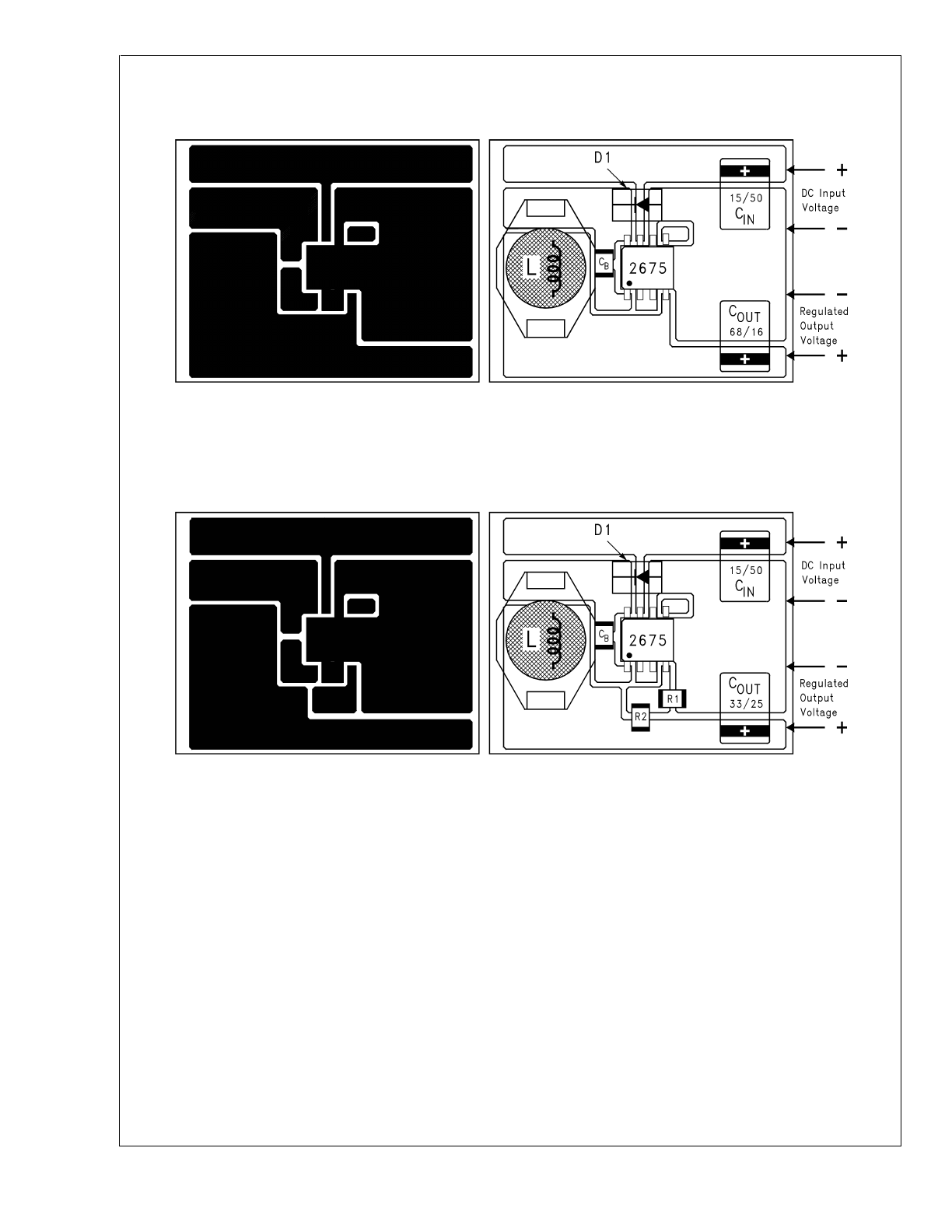
TYPICAL SURFACE MOUNT PC BOARD LAYOUT, FIXED OUTPUT (4X SIZE)
TYPICAL SURFACE MOUNT PC BOARD LAYOUT, ADJUSTABLE OUTPUT (4X SIZE)
Layout is very important in switching regulator designs. Rap-
idly switching currents associated with wiring inductance can
generate voltage transients which can cause problems. For
minimal inductance and ground loops, the wires indicated by
heavy lines (in
Figure 2
and
Figure 3
) should be wide
printed circuit traces and should be kept as short as
possible. For best results, external components should be
located as close to the switcher IC as possible using ground
plane construction or single point grounding.
If open core inductors are used, special care must be
taken as to the location and positioning of this type of induc-
tor. Allowing the inductor flux to intersect sensitive feedback,
IC ground path, and C
OUT
wiring can cause problems.
When using the adjustable version, special care must be
taken as to the location of the feedback resistors and the as-
sociated wiring. Physically locate both resistors near the IC,
and route the wiring away from the inductor, especially an
open core type of inductor.
DS012803-36
C
IN
- 15 µF, 50V, Solid Tantalum Sprague, “594D series”
C
OUT
- 68 µF, 16V, Solid Tantalum Sprague, “594D series”
D1 - 1A, 40V Schottky Rectifier, Surface Mount
L1 - 33 µH, L23, Coilcraft DO3316
C
B
- 0.01 µF, 50V, Ceramic
DS012803-37
C
IN
- 15 µF, 50V, Solid Tantalum Sprague, “594D series”
C
OUT
- 33 µF, 25V, Solid Tantalum Sprague, “594D series”
D1 - 1A, 40V Schottky Rectifier, Surface Mount
L1 - 68 µH, L30, Coilcraft DO3316
C
B
- 0.01 µF, 50V, Ceramic
R1 - 1k, 1%
R2 - Use formula in Design Procedure
FIGURE 18. PC Board Layout
LM2675
www.national.com
20
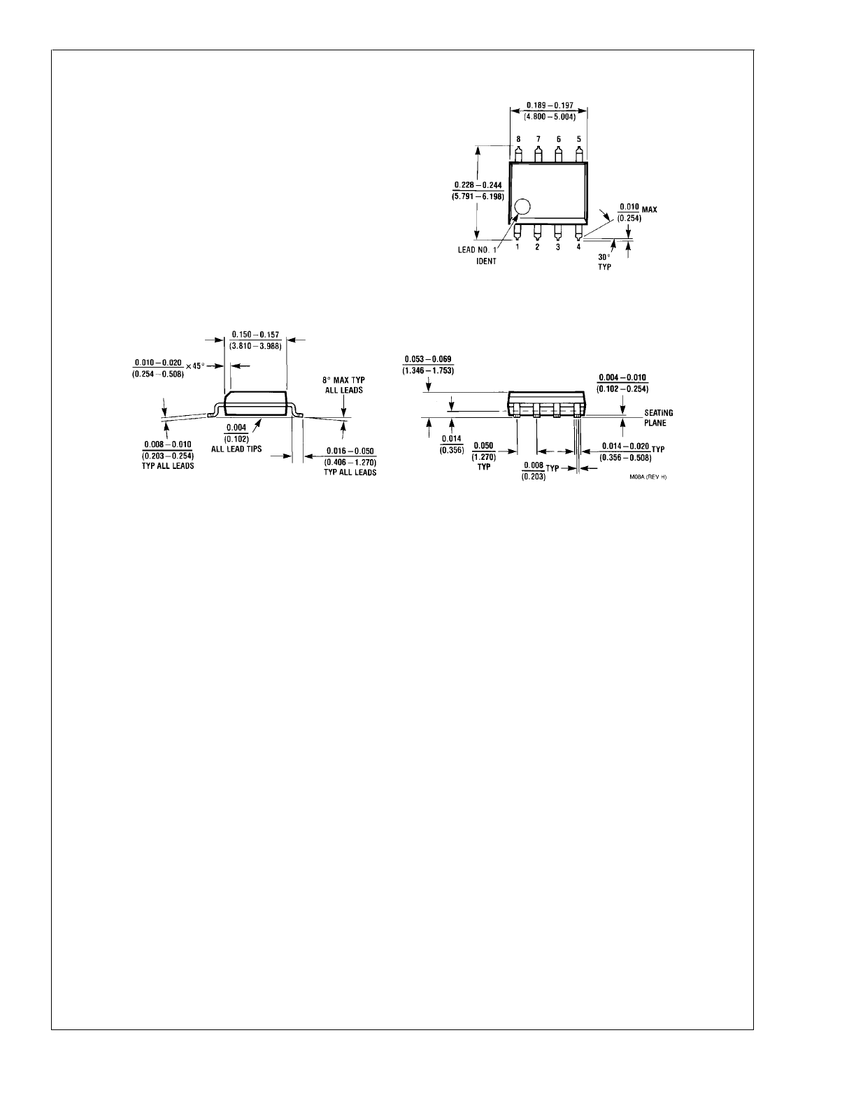
Physical Dimensions
inches (millimeters) unless otherwise noted
8-Lead (0.150" Wide) Molded Small Outline Package, JEDEC
Order Number LM2675M-3.3, LM2675M-5.0,
LM2675M-12 or LM2675M-ADJ
NS Package Number M08A
LM2675
www.national.com
21
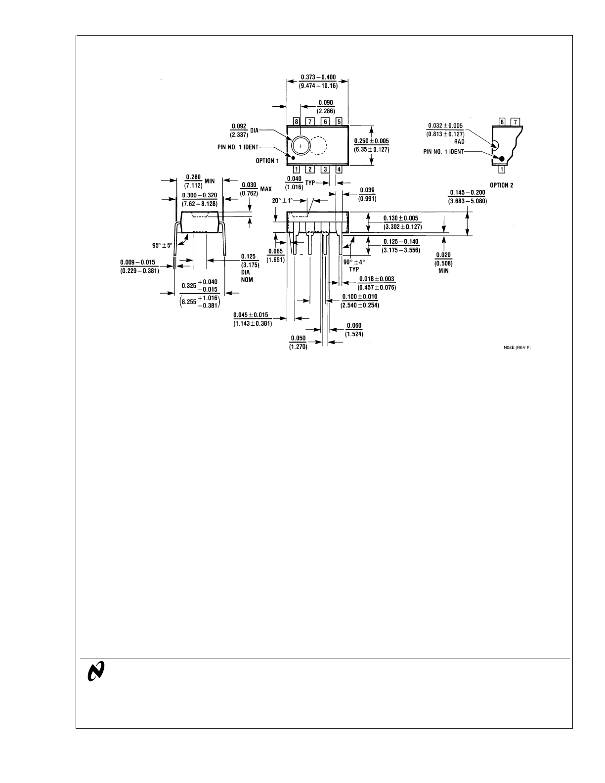
Physical Dimensions
inches (millimeters) unless otherwise noted (Continued)
LIFE SUPPORT POLICY
NATIONAL’S PRODUCTS ARE NOT AUTHORIZED FOR USE AS CRITICAL COMPONENTS IN LIFE SUPPORT
DEVICES OR SYSTEMS WITHOUT THE EXPRESS WRITTEN APPROVAL OF THE PRESIDENT AND GENERAL
COUNSEL OF NATIONAL SEMICONDUCTOR CORPORATION. As used herein:
1. Life support devices or systems are devices or
systems which, (a) are intended for surgical implant
into the body, or (b) support or sustain life, and
whose failure to perform when properly used in
accordance with instructions for use provided in the
labeling, can be reasonably expected to result in a
significant injury to the user.
2. A critical component is any component of a life
support device or system whose failure to perform
can be reasonably expected to cause the failure of
the life support device or system, or to affect its
safety or effectiveness.
National Semiconductor
Corporation
Americas
Tel: 1-800-272-9959
Fax: 1-800-737-7018
Email: support@nsc.com
National Semiconductor
Europe
Fax: +49 (0) 180-530 85 86
Email: europe.support@nsc.com
Deutsch Tel: +49 (0) 69 9508 6208
English
Tel: +44 (0) 870 24 0 2171
Français Tel: +33 (0) 1 41 91 8790
National Semiconductor
Asia Pacific Customer
Response Group
Tel: 65-2544466
Fax: 65-2504466
Email: ap.support@nsc.com
National Semiconductor
Japan Ltd.
Tel: 81-3-5639-7560
Fax: 81-3-5639-7507
www.national.com
8-Lead (0.300" Wide) Molded Dual-In-Line Package
Order Number LM2675N-3.3, LM2675N-5.0,
LM2675N-12 or LM2675N-ADJ
NS Package Number N08E
LM2675
SIMPLE
SWITCHER
Power
Converter
High
Efficiency
1A
Step-Down
V
oltage
Regulator
National does not assume any responsibility for use of any circuitry described, no circuit patent licenses are implied and National reserves the right at any time without notice to change said circuitry and specifications.