
TL/F/12009
74LVXC4245
8-Bit
Dual
Supply
Configurable
Voltage
Interface
Transceiver
with
TRI-STATE
Outputs
October 1995
74LVXC4245
8-Bit Dual Supply Configurable Voltage
Interface Transceiver with TRI-STATE
É
Outputs
General Description
The LVXC4245 is a 24-pin dual-supply, 8-bit configurable
voltage interface transceiver suited for PCMCIA and other
real time configurable I/O applications. The V
CCA
pin ac-
cepts a 5V supply level. The ‘‘A’’ port is a dedicated 5V port.
The V
CCB
pin accepts a 3V-to-5V supply level. The ‘‘B’’ port
is configured to track the V
CCB
supply level respectively. A
5V level on the V
CC
pin will configure the I/O pins at a 5V
level and a 3V V
CC
will configure the I/O pins at a 3V level.
This device will allow the V
CCB
voltage source pin and I/O
pins on the ‘‘B’’ port to float when OE is HIGH. This feature
is necessary to buffer data to and from a PCMCIA socket
that permits PCMCIA cards to be inserted and removed dur-
ing normal operation.
Features
Y
Bidirectional interface between 5V and 3V-to-5V buses
Y
Control inputs compatible with TTL level
Y
Outputs source/sink up to 24 mA
Y
Guaranteed simultaneous switching noise level and dy-
namic threshold performance
Y
Available in SOIC, QSOP and TSSOP packages
Y
Implements patented Quiet Series EMI reduction
circuitry
Y
Flexible V
CCB
operating range
Y
Allows B port and V
CCB
to float simultaneously when
OE is HIGH
Y
Functionally compatible with the 74 series 245
Logic Symbol
TL/F/12009 – 1
Pin Names
Description
OE
Output Enable Input
T/R
Transmit/Receive Input
A
0
– A
7
Side A Inputs or TRI-STATE Outputs
B
0
– B
7
Side B Inputs or TRI-STATE Outputs
Connection Diagram
Pin Assignment
for SOIC, QSOP and TSSOP
TL/F/12009 – 2
SOIC JEDEC
QSOP
TSSOP
Order Number
74LVXC4245WM
74LVXC4245QSC
74LVXC4245MTC
74LVXC4245WMX
74LVXC4245QSCX
74LVXC4245MTCX
See NS Package Number
M24B
MQA24
MTC24
TRI-STATE
É
is a registered trademark of National Semiconductor Corporation.
C1995 National Semiconductor Corporation
RRD-B30M115/Printed in U. S. A.
Truth Table
Inputs
Outputs
OE
T/R
L
L
Bus B Data to Bus A
L
H
Bus A Data to Bus B
H
X
HIGH-Z State
Logic Diagram
TL/F/12009 – 4
2
Absolute Maximum Ratings
(Note)
If Military/Aerospace specified devices are required,
please contact the National Semiconductor Sales
Office/Distributors for availability and specifications.
Supply Voltage (V
CCA
,V
CCB
)
b
0.5V to
a
7.0V
DC Input Voltage (V
I
)
@
OE, T/R
b
0.5V to V
CCA
a
0.5V
DC Input/Output Voltage (V
I/O
)
@
A
n
b
0.5V to V
CCA
a
0.5V
@
B
n
b
0.5V to V
CCB
a
0.5V
DC Input Diode Current (I
IK
)
@
OE, T/R
g
20 mA
DC Output Diode Current (I
OK
)
g
50 mA
DC Output Source or Sink Current (I
O
)
g
50 mA
DC V
CC
or Ground Current
Per Output Pin (I
CC
or I
GND
)
g
50 mA
and Max Current
g
200 mA
Storage Temperature Range (T
STG
)
b
65
§
C to
a
150
§
C
DC Latch-Up Source or Sink Current
g
300 mA
Recommended Operating
Conditions
Supply Voltage
V
CCA
4.5V to 5.5V
V
CCB
2.7V to 5.5V
Input Voltage (V
I
)
@
OE, T/R
0V to V
CCA
Input/Output Voltage (V
I/O
)
@
A
n
0V to V
CCA
@
B
n
0V to V
CCB
Free Air Operating Temperature (T
A
)
b
40
§
C to
a
85
§
C
Minimum Input Edge Rate (DV/Dt)
8 ns/V
V
IN
from 30% to 70% of V
CC
V
CC
@
3V, 4.5V, 5.5V
Note:
The ‘‘Absolute Maximum Ratings’’ are those values
beyond which the safety of the device cannot be guaran-
teed. The device should not be operated at these limits. The
parametric values defined in the ‘‘Electrical Characteristics’’
table are not guaranteed at the absolute maximum ratings.
The ‘‘Recommended Operating Conditions’’ table will define
the conditions for actual device operation
.
DC Electrical Characteristics
Symbol
Parameter
V
CCA
(V)
V
CCB
(V)
74LVXC4245
Units
Conditions
T
A
e a
25
§
C
T
A
e b
40
§
C to
a
85
§
C
Typ
Guaranteed Limits
V
IHA
Minimum High Level
A
n
4.5
2.7
2.0
2.0
V
V
OUT
s
0.1V
Input Voltage
OE
4.5
3.6
2.0
2.0
or
T/R
5.5
5.5
2.0
2.0
t
V
CC
b
0.1V
V
IHB
B
n
4.5
2.7
2.0
2.0
4.5
3.6
2.0
2.0
4.5
5.5
3.85
3.85
V
ILA
Maximum Low Level
A
n
4.5
2.7
0.8
0.8
V
V
OUT
s
0.1V
Input Voltage
OE
4.5
3.6
0.8
0.8
or
T/R
5.5
5.5
0.8
0.8
t
V
CC
b
0.1V
V
ILB
B
n
4.5
2.7
0.8
0.8
4.5
3.6
0.8
0.8
4.5
5.5
1.65
1.65
V
OHA
Minimum High Level
4.5
3.0
4.49
4.4
4.4
V
I
OUT
e b
100 mA
Output Voltage
4.5
3.0
4.25
3.86
3.76
I
OH
e b
24 mA
V
OHB
4.5
3.0
2.99
2.9
2.9
V
I
OUT
e b
100 mA
4.5
3.0
2.85
2.56
2.46
I
OH
e b
12 mA
4.5
3.0
2.65
2.35
2.25
I
OH
e b
24 mA
4.5
2.7
2.5
2.3
2.2
I
OH
e b
12 mA
4.5
2.7
2.3
2.1
2.0
I
OH
e b
24 mA
4.5
4.5
4.25
3.86
3.76
I
OH
e b
24 mA
V
OLA
Maximum Low Level
4.5
3.0
0.002
0.1
0.1
V
I
OUT
e
100 mA
Output Voltage
4.5
3.0
0.21
0.36
0.44
I
OL
e
24 mA
V
OLB
4.5
3.0
0.002
0.1
0.1
V
I
OUT
e
100 mA
4.5
3.0
0.21
0.36
0.44
I
OL
e
24 mA
4.5
2.7
0.11
0.36
0.44
I
OL
e
12 mA
4.5
2.7
0.22
0.42
0.5
I
OL
e
24 mA
4.5
4.5
0.18
0.36
0.44
I
OL
e
24 mA
3
DC Electrical Characteristics
(Continued)
Symbol
Parameter
V
CCA
(V)
V
CCB
(V)
74LVXC4245
Units
Conditions
T
A
e a
25
§
C
T
A
e b
40
§
C to
a
85
§
C
Typ
Guaranteed Limits
I
IN
Maximum Input
5.5
3.6
g
0.1
g
1.0
m
A
V
I
e
V
CCA
, GND
Leakage Current
@
5.5
5.5
g
0.1
g
1.0
OE, T/R
I
OZA
Maximum TRI-STATE
5.5
3.6
g
0.5
g
5.0
m
A
V
I
e
V
IL
, V
IH
, OE
e
V
CCA
Output Leakage
@
A
n
5.5
5.5
g
0.5
g
5.0
V
O
e
V
CCA
, GND
I
OZB
Maximum TRI-STATE
5.5
3.6
g
0.5
g
5.0
m
A
V
I
e
V
IL
, V
IH
, OE
e
V
CCA
Output Leakage
@
B
n
5.5
5.5
g
0.5
g
5.0
V
O
e
V
CCB
, GND
D
I
CC
Maximum
All Inputs
5.5
5.5
1.0
1.35
1.5
mA
V
I
e
V
CC
b
2.1V
I
CC
/Input
B
n
5.5
3.6
0.35
0.5
mA
V
I
e
V
CCB
b
0.6V
I
CCA1
Quiescent V
CCA
A
n
e
V
CCA
or GND
Supply Current as B
5.5
Open
8
80
m
A
B
n
e
Open, OE
e
V
CCA
Port Floats
T/R
e
V
CCA
, V
CCB
e
Open
I
CCA2
Quiescent V
CCA
5.5
3.6
8
80
A
n
e
V
CCA
or GND
Supply Current
5.5
5.5
8
80
m
A
B
n
e
V
CCB
or GND
OE
e
GND, T/R
e
GND
I
CCB
Quiescent V
CCB
5.5
3.6
5
50
A
n
e
V
CCA
or GND
Supply Current
5.5
5.5
8
80
m
A
B
n
e
V
CCB
or GND
OE
e
GND, T/R
e
V
CCA
V
OLPA
Quiet Output
5.0
3.3
1.5
V
(Notes 1 and 2)
Maximum Dynamic
5.0
5.0
1.5
V
OL
V
OLPB
5.0
3.3
0.8
V
(Notes 1 and 2)
5.0
5.0
1.5
V
OLVA
Quiet Output Minimum
5.0
3.3
b
1.2
V
(Notes 1 and 2)
Dynamic V
OL
5.0
5.0
b
1.2
V
OLVB
5.0
3.3
b
0.8
V
(Notes 1 and 2)
5.0
5.0
b
1.2
V
IHDA
Minimum High Level
5.0
3.3
2.0
V
(Notes 1 and 3)
Dynamic Input
5.0
5.0
2.0
Voltage
V
IHDB
5.0
3.3
2.0
V
(Notes 1 and 3)
5.0
5.0
3.5
V
ILDA
Maximum Low Level
5.0
3.3
0.8
V
(Notes 1 and 3)
Dynamic Input
5.0
5.0
0.8
Voltage
V
ILDB
5.0
3.3
0.8
V
(Notes 1 and 3)
5.0
5.0
1.5
Note 1:
Worst case package.
Note 2:
Max number of outputs defined as (n). Data inputs are driven 0V to V
CC
level; one output at GND.
Note 3:
Max number of Data Inputs (n) switching. (nb1) inputs switching 0V to V
CC
level. Input-under-test switching: V
CC
level to threshold (V
IHD
), 0V to threshold
(V
ILD
), f e 1 MHz.
4
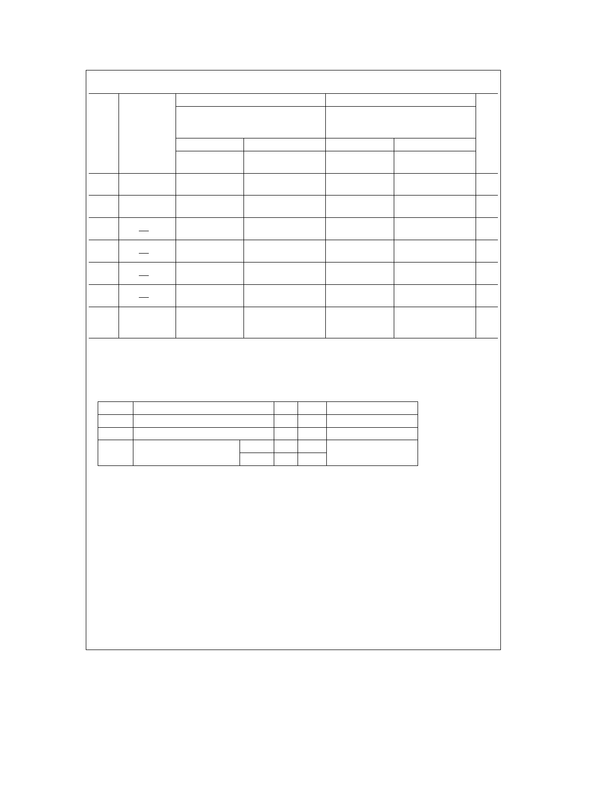
AC Electrical Characteristics
Symbol
Parameter
74LVXC4245
74LVXC4245
Units
C
L
e
50 pF
C
L
e
50 pF
V
CCA
e
4.5V to 5.5V
V
CCA
e
4.5V to 5.5V
V
CCB
e
4.5V to 5.5V
V
CCB
e
2.7V to 3.6V
T
A
e a
25
§
C
T
A
e b
40
§
C to
a
85
§
C
T
A
e a
25
§
C
T
A
e b
40
§
C to
a
85
§
C
Min
Typ
Max
Min
Max
Min
Typ
Max
Min
Max
(Note 1)
(Note 2)
t
PHL
Propagation
1.0
4.9
6.5
1.0
7.0
1.0
5.5
7.5
1.0
8.0
ns
t
PLH
Delay A to B
1.0
4.0
5.5
1.0
6.0
1.0
5.0
7.0
1.0
7.5
t
PHL
Propagation
1.0
4.7
6.5
1.0
7.0
1.0
5.6
7.5
1.0
8.0
ns
t
PLH
Delay B to A
1.0
3.9
5.0
1.0
5.5
1.0
4.3
6.0
1.0
6.5
t
PZL
Output Enable
1.0
5.6
7.5
1.0
8.0
1.0
6.7
9.0
1.0
10.0
ns
t
PZH
Time OE to B
1.0
5.7
7.5
1.0
8.0
1.0
6.9
9.5
1.0
10.0
t
PZL
Output Enable
1.0
7.4
9.0
1.0
10.0
1.0
8.0
10.0
1.0
11.0
ns
t
PZH
Time OE to A
1.0
6.1
7.5
1.0
8.5
1.0
6.3
8.0
1.0
8.5
t
PHZ
Output Disable
1.0
4.8
7.0
1.0
7.5
1.0
6.0
9.0
1.0
9.5
ns
t
PLZ
Time OE to B
1.0
3.8
5.5
1.0
6.0
1.0
4.2
6.5
1.0
7.0
t
PHZ
Output Disable
1.0
3.4
5.5
1.0
6.0
1.0
3.4
5.5
1.0
6.0
ns
t
PLZ
Time OE to A
1.0
2.9
4.5
1.0
5.0
1.0
2.9
5.0
1.0
5.5
t
OSHL
Output to Output
t
OSLH
Skew (Note 3)
1.0
1.5
1.5
1.0
1.5
1.5
ns
Data to Output
Note 1:
Typical values at V
CCA
e
5V, V
CCB
e
5V
@
25
§
C.
Note 2:
Typical values at V
CCA
e
5V, V
CCB
e
3.3V
@
25
§
C.
Note 3:
Skew is defined as the absolute value of the difference between the actual propagation delay for any two separate outputs of the same device. The
specification applies to any outputs switching in the same direction, either HIGH to LOW (t
OSHL
) or LOW to HIGH (t
OSLH
). Parameter guaranteed by design.
Capacitance
Symbol
Parameter
Typ
Units
Conditions
C
IN
Input Capacitance
4.5
pF
V
CC
e
Open
C
I/O
Input/Output Capacitance
10
pF
V
CCA
e
5V, V
CCB
e
3.3V
C
PD
Power Dissipation Capacitance
A
x
B
45
pF
V
CCA
e
5V
B
x
A
50
pF
V
CCB
e
3.3V
Note:
C
PD
is measured at 10 MHz.
5
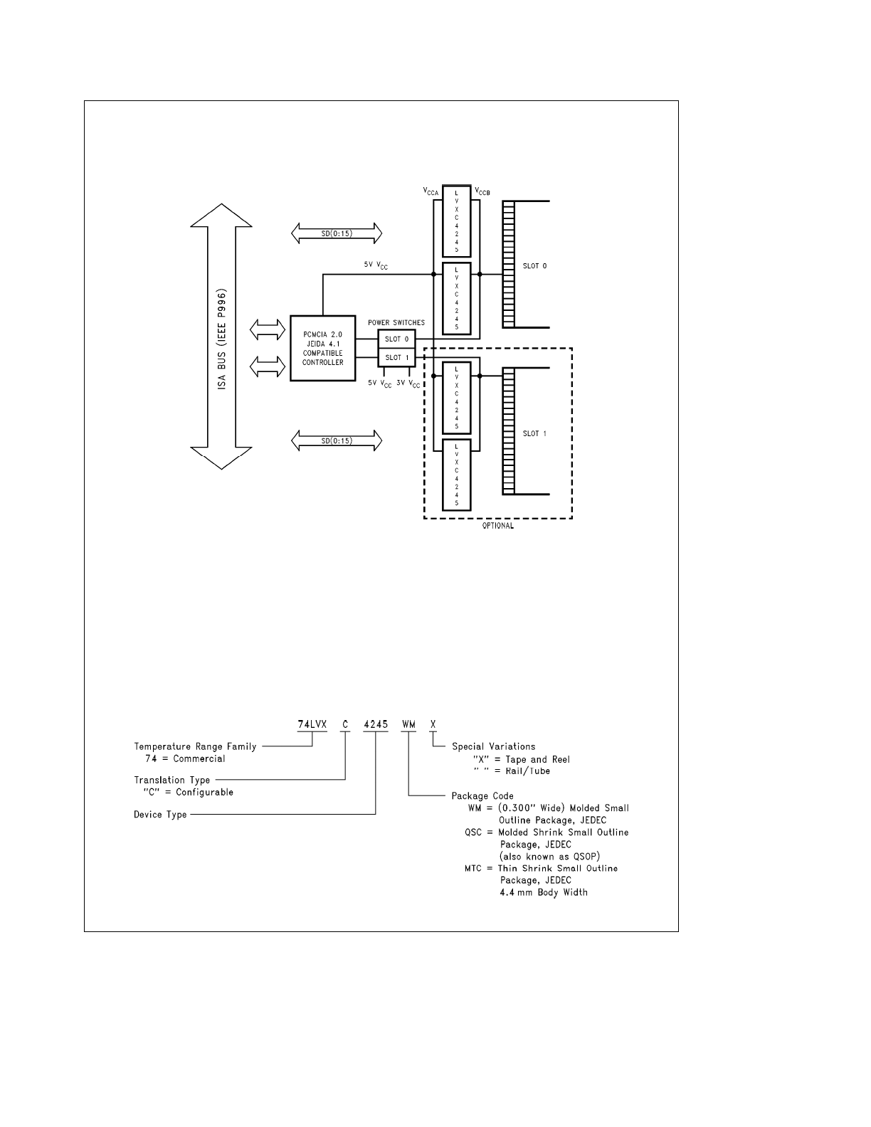
Configurable I/O Application for PCMCIA Cards
Block Diagram
74LVXC4245
TL/F/12009 – 3
The LVXC4245 is a 24-pin dual supply device well suited for
PCMCIA configurable I/O applications. Ideal for low power
notebook designs, the LVXC4245 consumes less than
1 mW of quiescent power in all modes of operation. The
LVXC4245 meets all PCMCIA I/O voltage requirements at
5V and 3.3V operation. By tying V
CCB
of the LVXC4245 to
the card voltage supply, the PCMCIA card will always expe-
rience rail to rail output swings, maximizing the reliability of
the interface.
The V
CCA
pin on the LVXC4245 must always be tied to a 5V
power supply. This voltage connection provides internal ref-
erences needed to account for variations in V
CCB
. When
connected as in the block diagram above, the LVXC4245
meets all the voltage and current requirements of the ISA
bus standard (IEEE P996).
74LVXC4245 Ordering Information
The device number is used to form part of a simplified purchasing code where the package type and temperature range are
defined as follows:
TL/F/12009 – 6
6
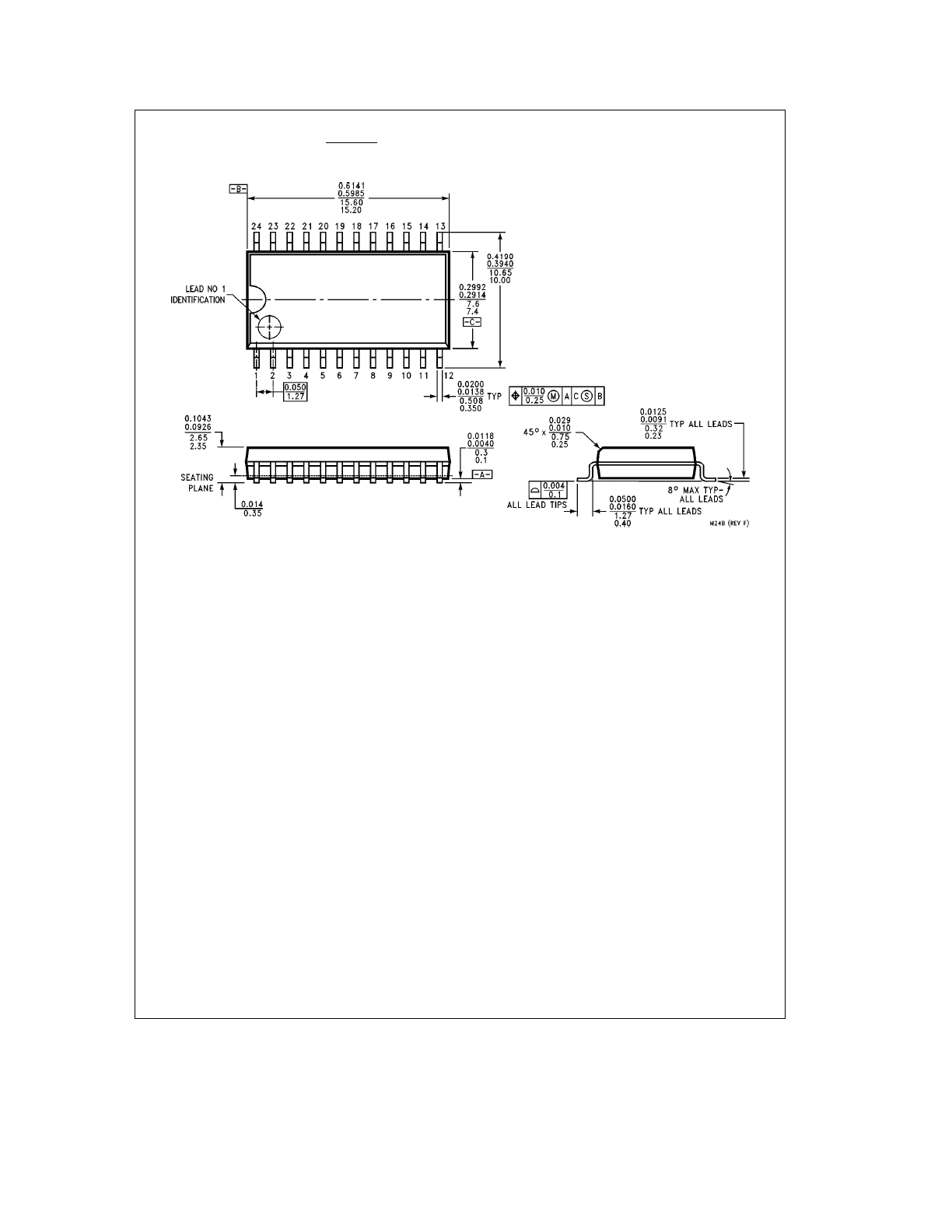
Physical Dimensions
inches
millimeters
24-Lead (0.300
×
Wide) Molded Small Outline Package, JEDEC
Order Number 74LVXC4245WM or 74LVXC4245WMX
NS Package Number M24B
7
74LVXC4245
8-Bit
Dual
Supply
Configurable
Voltage
Interface
Transceiver
with
TRI-STATE
Outputs
Physical Dimensions
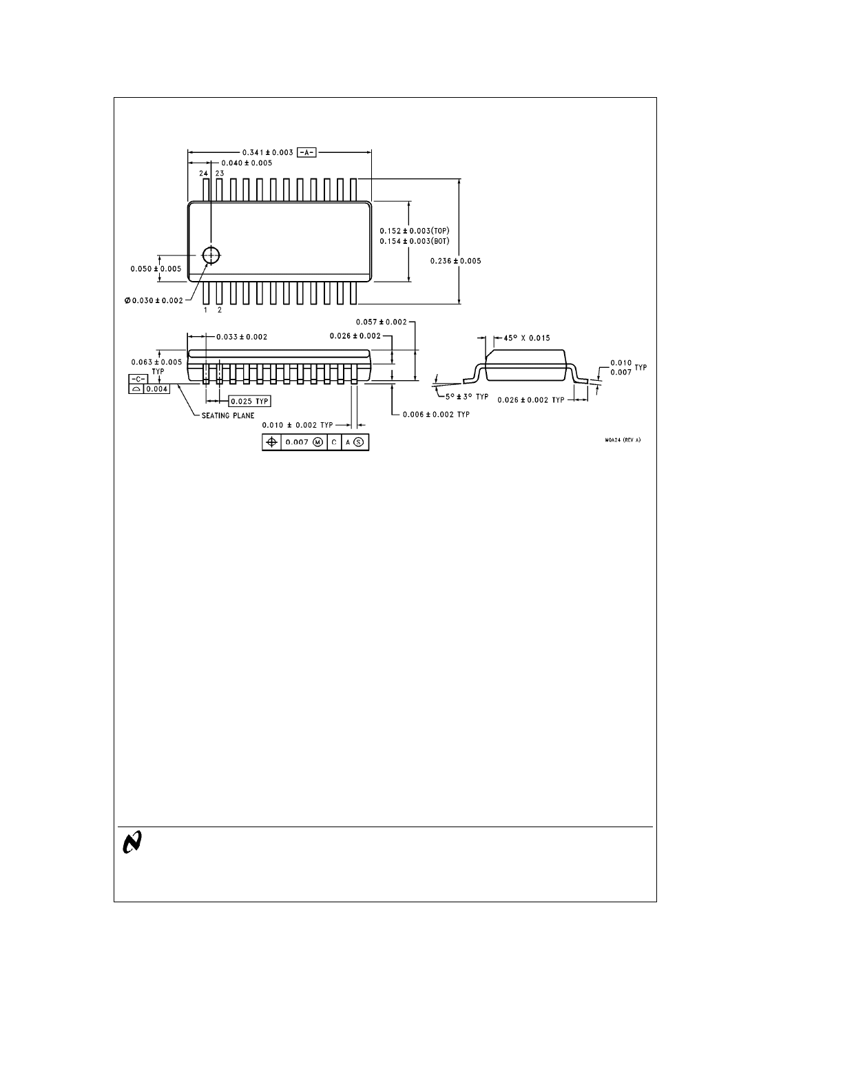
inches (Continued)
24-Lead (0.150
×
Wide) Molded Shrink Small Outline Package, JEDEC
(also known as QSOP)
Order Number 74LVXC4245QSC or 74LVXC4245QSCX
NS Package Number MQA24
LIFE SUPPORT POLICY
NATIONAL’S PRODUCTS ARE NOT AUTHORIZED FOR USE AS CRITICAL COMPONENTS IN LIFE SUPPORT
DEVICES OR SYSTEMS WITHOUT THE EXPRESS WRITTEN APPROVAL OF THE PRESIDENT OF NATIONAL
SEMICONDUCTOR CORPORATION. As used herein:
1. Life support devices or systems are devices or
2. A critical component is any component of a life
systems which, (a) are intended for surgical implant
support device or system whose failure to perform can
into the body, or (b) support or sustain life, and whose
be reasonably expected to cause the failure of the life
failure to perform, when properly used in accordance
support device or system, or to affect its safety or
with instructions for use provided in the labeling, can
effectiveness.
be reasonably expected to result in a significant injury
to the user.
National Semiconductor
National Semiconductor
National Semiconductor
National Semiconductor
Corporation
Europe
Hong Kong Ltd.
Japan Ltd.
1111 West Bardin Road
Fax: (
a
49) 0-180-530 85 86
13th Floor, Straight Block,
Tel: 81-043-299-2309
Arlington, TX 76017
Email: cnjwge
@
tevm2.nsc.com
Ocean Centre, 5 Canton Rd.
Fax: 81-043-299-2408
Tel: 1(800) 272-9959
Deutsch Tel: (
a
49) 0-180-530 85 85
Tsimshatsui, Kowloon
Fax: 1(800) 737-7018
English
Tel: (
a
49) 0-180-532 78 32
Hong Kong
Fran
3ais Tel: (
a
49) 0-180-532 93 58
Tel: (852) 2737-1600
Italiano
Tel: (
a
49) 0-180-534 16 80
Fax: (852) 2736-9960
National does not assume any responsibility for use of any circuitry described, no circuit patent licenses are implied and National reserves the right at any time without notice to change said circuitry and specifications.