
TL/F/12405
74LCX573
Low
Voltage
Octal
Latch
with
5V
Tolerant
Inputs
and
Outputs
October 1995
74LCX573
Low Voltage Octal Latch with 5V
Tolerant Inputs and Outputs
General Description
The ’LCX573 is a high-speed octal latch with buffered com-
mon Latch Enable (LE) and buffered common Output En-
able (OE) inputs.
The ’LCX573 is functionally identical to the ’LCX373 but has
inputs and outputs on opposite sides.
The ’LCX573 is designed for low voltage (3.3V) applications
with capability of interfacing to a 5V signal environment. The
’LCX573 is fabricated with an advanced CMOS technology
to achieve high speed operation while maintaining CMOS
low power dissipation.
Features
Y
5V tolerant inputs and outputs
Y
7.0 ns t
PD
max, 10 mA I
CCQ
max
Y
Power down high impedance inputs and outputs
Y
Supports live insertion/withdrawal
Y
2.0V – 3.6V V
CC
supply operation
Y
g
24 mA output drive
Y
Implements patented Quiet Series
TM
noise/EMI reduc-
tion circuitry
Y
Functionally compatible with 74 series 573
Y
Latch-up performance exceeds 500 mA
Y
ESD performance:
Human body model
l
2000V
Machine model
l
200V
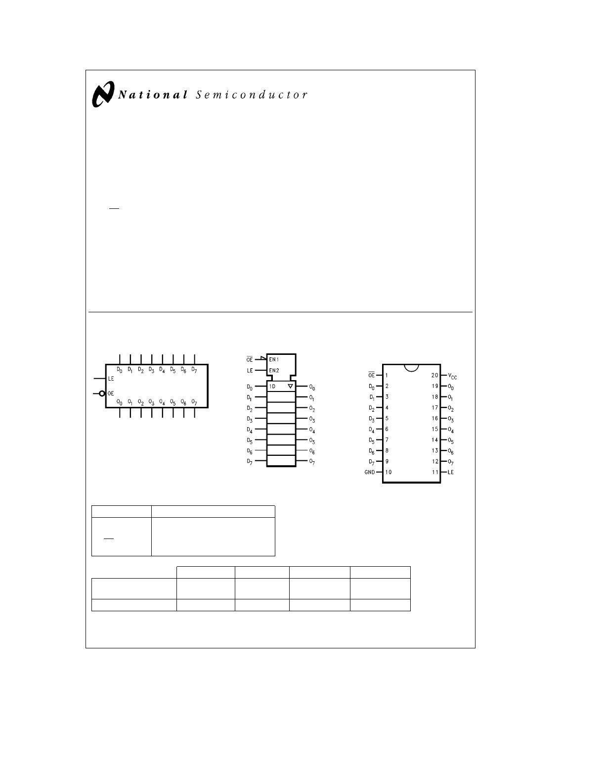
Logic Symbols
TL/F/12405 – 1
IEEE/IEC
TL/F/12405 – 2
Connection Diagrams
Pin Assignment
for SOIC, SSOP and TSSOP
TL/F/12405 – 3
Pin Names
Description
D
0
– D
7
Data Inputs
LE
Latch Enable Input
OE
TRI-STATE Output Enable Input
O
0
– O
7
TRI-STATE Latch Outputs
SOIC JEDEC
SOIC EIAJ
SSOP TYPE II
TSSOP JEDEC
Order Number
74LCX573WM
74LCX573SJ
74LCX573MSA
74LCX573MTC
74LCX573WMX
74LCX573SJX
74LCX573MSAX
74LCX573MTCX
See NS Package Number
M20B
M20D
MSA20
MTC20
TRI-STATE
É
is a registered trademark of National Semiconductor Corporation.
Quiet Series
TM
is a trademark of National Semiconductor Corporation.
C1995 National Semiconductor Corporation
RRD-B30M115/Printed in U. S. A.
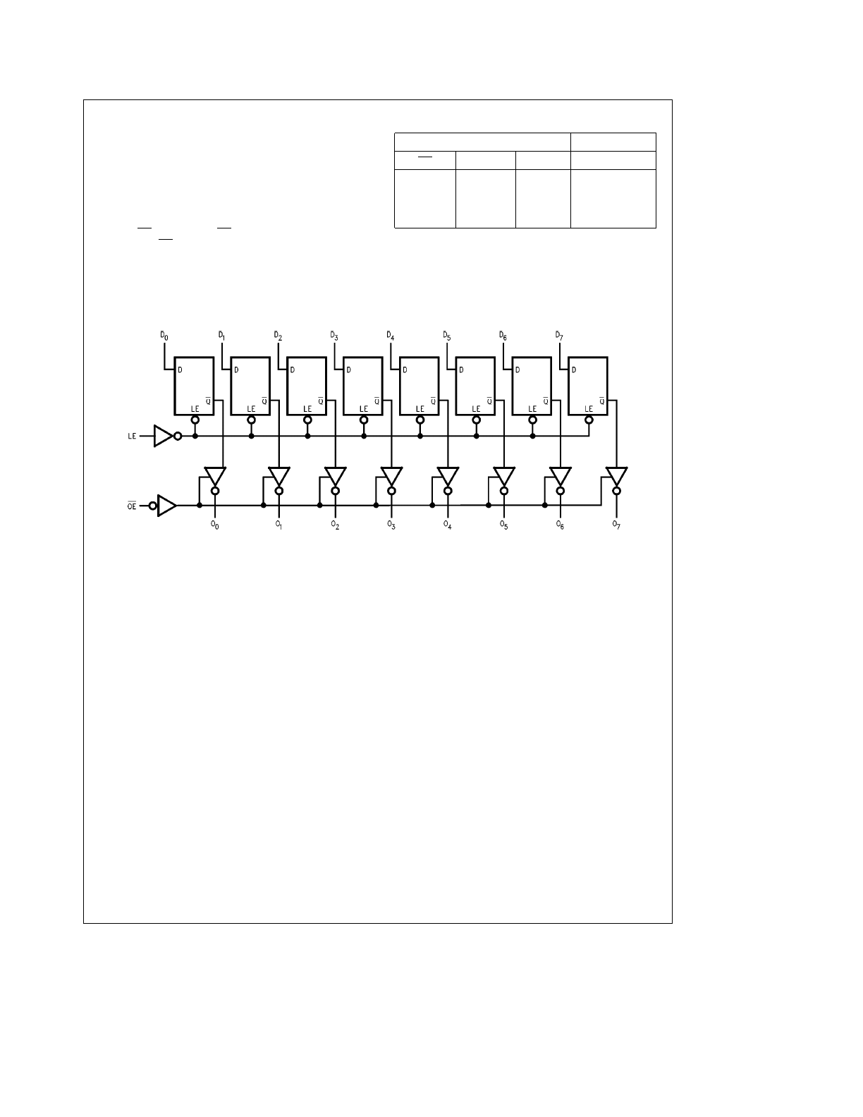
Functional Description
The ’LCX573 contains eight D-type latches with TRI-STATE
output buffers. When the Latch Enable (LE) input is HIGH,
data on the D
n
inputs enters the latches. In this condition
the latches are transparent, i.e., a latch output will change
state each time its D input changes. When LE is LOW the
latches store the information that was present on the D in-
puts a setup time preceding the HIGH-to-LOW transition of
LE. The TRI-STATE buffers are controlled by the Output
Enable (OE) input. When OE is LOW, the buffers are en-
abled. When OE is HIGH the buffers are in the high imped-
ance mode but this does not interfere with entering new
data into the latches.
Truth Table
Inputs
Outputs
OE
LE
D
O
n
L
H
H
H
L
H
L
L
L
L
X
O
0
H
X
X
Z
H e HIGH Voltage
L e LOW Voltage
Z e High Impedance
X e Immaterial
O
0
e
Previous O
0
before HIGH-to-LOW transition of Latch Enable
Logic Diagram
TL/F/12405 – 5
Please note that this diagram is provided only for the understanding of logic operations and should not be used to estimate propagation delays.
2
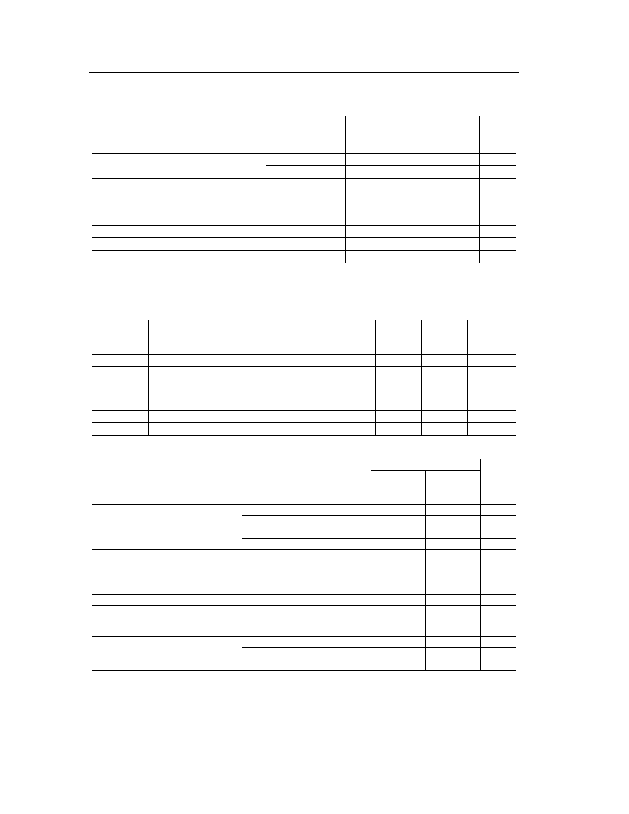
Absolute Maximum Ratings
(Note 1)
If Military/Aerospace specified devices are required, please contact the National Semiconductor Sales Office/
Distributors for availability and specifications.
Symbol
Parameter
Value
Conditions
Units
V
CC
Supply Voltage
b
0.5 to
a
7.0
V
V
I
DC Input Voltage
b
0.5 to
a
7.0
V
V
O
DC Output Voltage
b
0.5 to
a
7.0
Output in TRI-STATE
V
b
0.5 to V
CC
a
0.5
Output in High or Low State (Note 2)
V
I
IK
DC Input Diode Current
b
50
V
I
k
GND
mA
I
OK
DC Output Diode Current
b
50
V
O
k
GND
mA
a
50
V
O
l
V
CC
I
O
DC Output Source/Sink Current
g
50
mA
I
CC
DC Supply Current per Supply Pin
g
100
mA
I
GND
DC Ground Current per Ground Pin
g
100
mA
T
STG
Storage Temperature
b
65 to
a
150
§
C
Note 1:
The Absolute Maximum Ratings are those values beyond which the safety of the device cannot be guaranteed. The device should not be operated at these
limits. The parametric values defined in the ‘‘Electrical Characteristics’’ table are not guaranteed at the Absolute Maximum Ratings. The ‘‘Recommended Operating
Conditions’’ table will define the conditions for actual device operation.
Note 2:
I
O
Absolute Maximum Rating must be observed.
Recommended Operating Conditions
Symbol
Parameter
Min
Max
Units
V
CC
Supply Voltage
Operating
2.0
3.6
V
Data Retention
1.5
3.6
V
I
Input Voltage
0
5.5
V
V
O
Output Voltage
HIGH or LOW State
0
V
CC
V
TRI-STATE
0
5.5
I
OH
/I
OL
Output Current
V
CC
e
3.0V
b
3.6V
g
24
mA
V
CC
e
2.7V
g
12
T
A
Free-Air Operating Temperature
b
40
85
§
C
D
t/DV
Input Edge Rate, V
IN
e
0.8V – 2.0V, V
CC
e
3.0V
0
10
ns/V
DC Electrical Characteristics
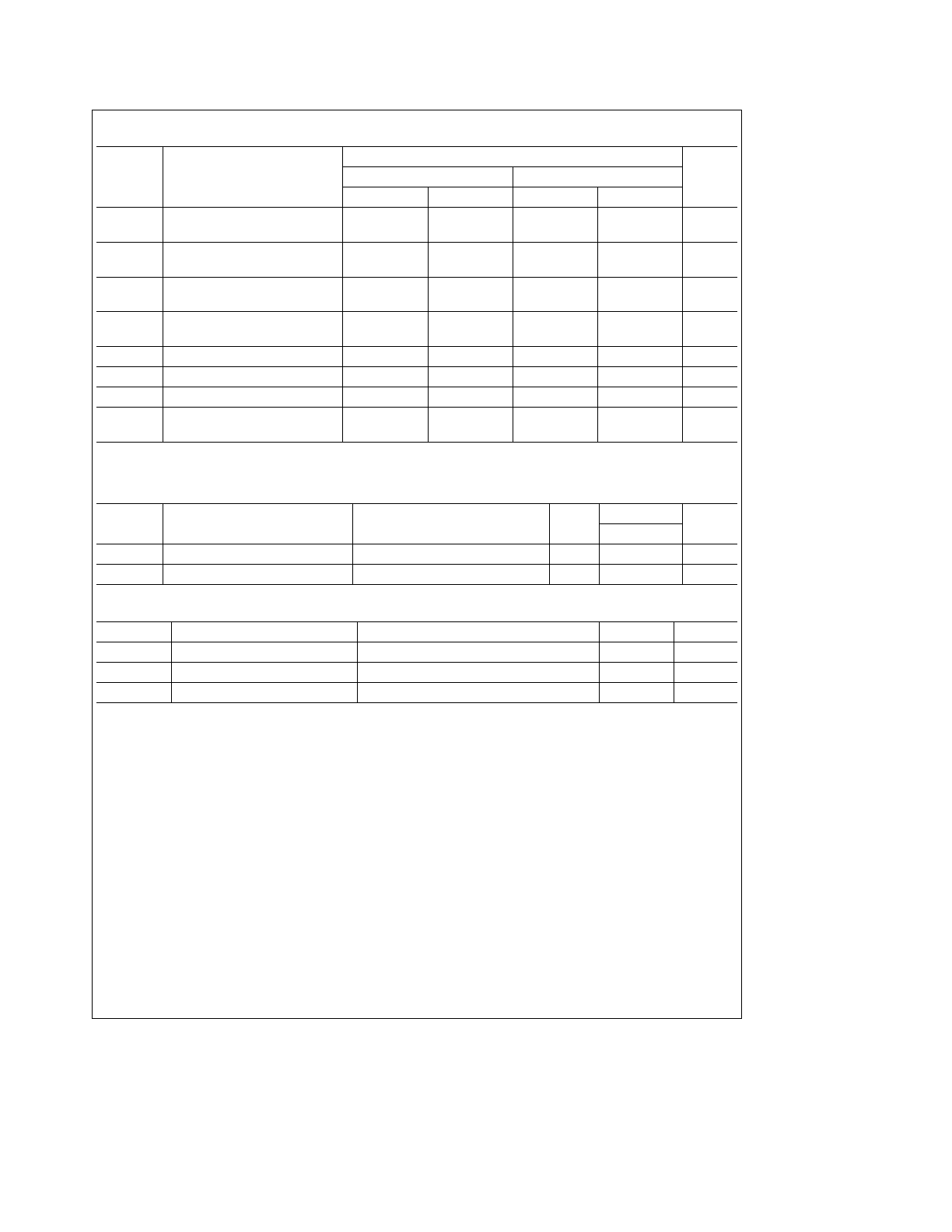
Symbol
Parameter
Conditions
V
CC
T
A
e b
40
§
C to
a
85
§
C
Units
(V)
Min
Max
V
IH
HIGH Level Input Voltage
2.7 – 3.6
2.0
V
V
IL
LOW Level Input Voltage
2.7 – 3.6
0.8
V
V
OH
HIGH Level Output Voltage
I
OH
e b
100 mA
2.7 – 3.6
V
CC
b
0.2
V
I
OH
e b
12 mA
2.7
2.2
V
I
OH
e b
18 mA
3.0
2.4
V
I
OH
e b
24 mA
3.0
2.2
V
V
OL
LOW Level Output Voltage
I
OL
e
100 mA
2.7 – 3.6
0.2
V
I
OL
e
12 mA
2.7
0.4
V
I
OL
e
16 mA
3.0
0.4
V
I
OL
e
24 mA
3.0
0.55
V
I
I
Input Leakage Current
0
s
V
I
s
5.5V
2.7 – 3.6
g
5.0
m
A
I
OZ
TRI-STATE Output Leakage
0
s
V
O
s
5.5V
2.7 – 3.6
g
5.0
m
A
V
I
e
V
IH
or V
IL
I
OFF
Power-Off Leakage Current
V
I
or V
O
e
5.5V
0
10
m
A
I
CC
Quiescent Supply Current
V
I
e
V
CC
or GND
2.7 – 3.6
10
m
A
3.6V
s
V
I
, V
O
s
5.5V
2.7 – 3.6
g
10
m
A
D
I
CC
Increase in I
CC
per Input
V
IH
e
V
CC
b
0.6V
2.7 – 3.6
500
m
A
3
AC Electrical Characteristics
Symbol
Parameter
T
A
e b
40
§
C to
a
85
§
C
Units
V
CC
e
3.3V
g
0.3V
V
CC
e
2.7V
Min
Max
Min
Max
t
PHL
Propagation Delay
1.5
8.0
1.5
9.0
ns
t
PLH
D
n
to O
n
1.5
8.0
1.5
9.0
t
PHL
Propagation Delay
1.5
8.5
1.5
9.5
ns
t
PLH
LE to O
n
1.5
8.5
1.5
9.5
t
PZL
Output Enable Time
1.5
8.5
1.5
9.5
ns
t
PZH
1.5
8.5
1.5
9.5
t
PLZ
Output Disable Time
1.5
6.5
1.5
7.0
ns
t
PHZ
1.5
6.5
1.5
7.0
t
S
Setup Time, D
n
to LE
2.5
2.5
ns
t
H
Hold Time, D
n
to LE
1.5
1.5
ns
t
W
LE Pulse Width
3.3
3.3
ns
t
OSHL
Output to Output Skew (Note 3)
1.0
ns
t
OSLH
1.0
Note 3:
Skew is defined as the absolute value of the difference between the actual propagation delay for any two separate outputs of the same device. The
specification applies to any outputs switching in the same direction, either HIGH to LOW (t
OSHL
) or LOW to HIGH (t
OSLH
).
Dynamic Switching Characteristics
Symbol
Parameter
Conditions
V
CC
(V)
T
A
e
25
§
C
Units
Typical
V
OLP
Quiet Output Dynamic Peak V
OL
C
L
e
50 pF, V
IH
e
3.3V, V
IL
e
0V
3.3
0.8
V
V
OLV
Quiet Output Dynamic Valley V
OL
C
L
e
50 pF, V
IH
e
3.3V, V
IL
e
0V
3.3
0.8
V
Capacitance
Symbol
Parameter
Conditions
Typical
Units
C
IN
Input Capacitance
V
CC
e
Open, V
I
e
0V or V
CC
7
pF
C
OUT
Output Capacitance
V
CC
e
3.3V, V
I
e
0V or V
CC
8
pF
C
PD
Power Dissipation Capacitance
V
CC
e
3.3V, V
I
e
0V or V
CC
, F
e
10 MHz
25
pF
4
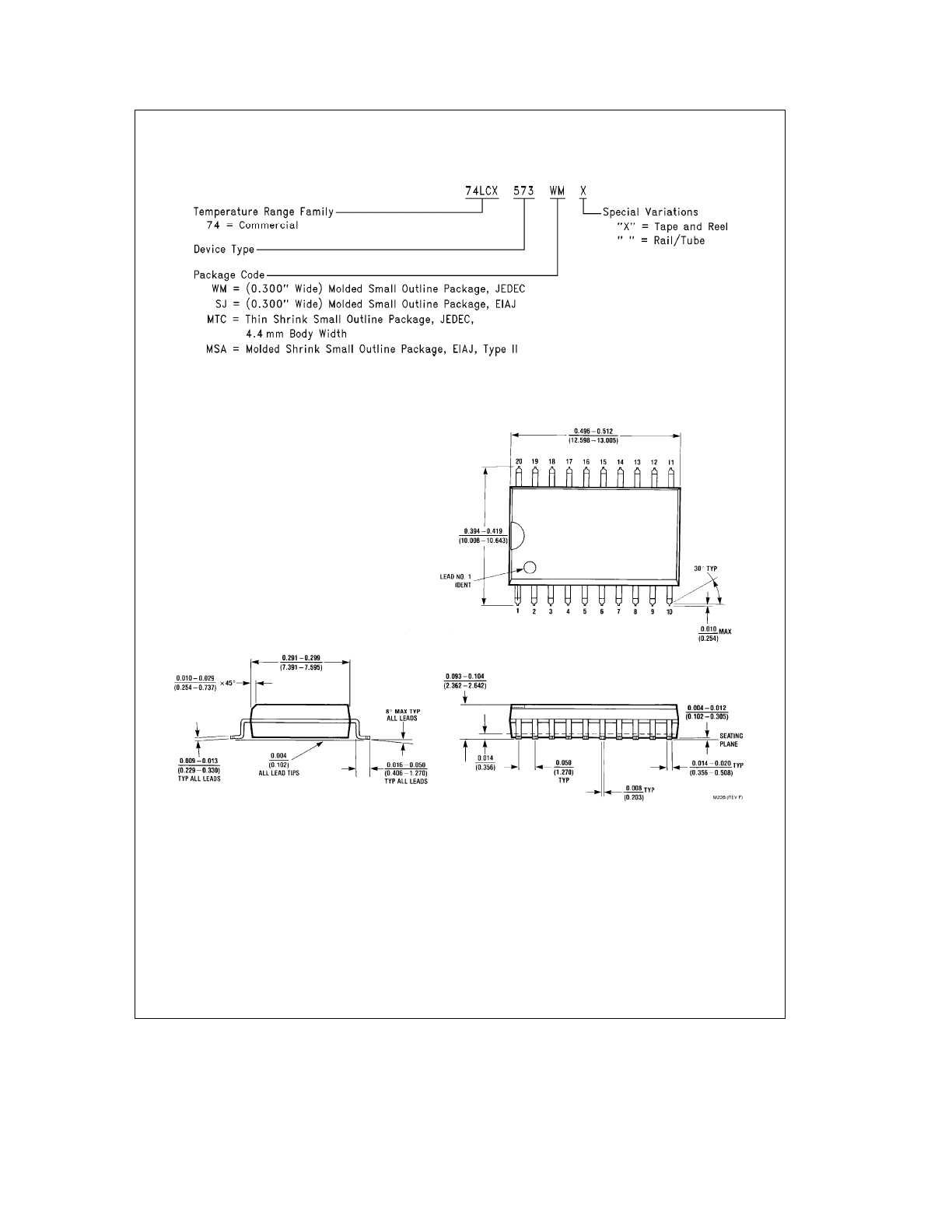
74LCX573 Ordering Information
The device number is used to form part of a simplified purchasing code where the package type and temperature range are
defined as follows:
TL/F/12405 – 6
Physical Dimensions
All dimensions are in inches (millimeters)
20-Lead (0.300
×
Wide) Molded Small Outline Package, JEDEC
Order Number 74LCX573WM or 74LCX573WMX
NS Package Number M20B
5
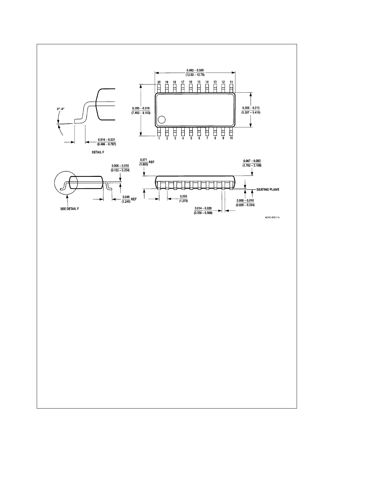
Physical Dimensions
All dimensions are in inches (millimeters) (Continued)
20-Lead (0.300
×
Wide) Molded Small Outline Package, EIAJ
Order Number 74LCX573SJ or 74LCX573SJX
NS Package Number M20D
6
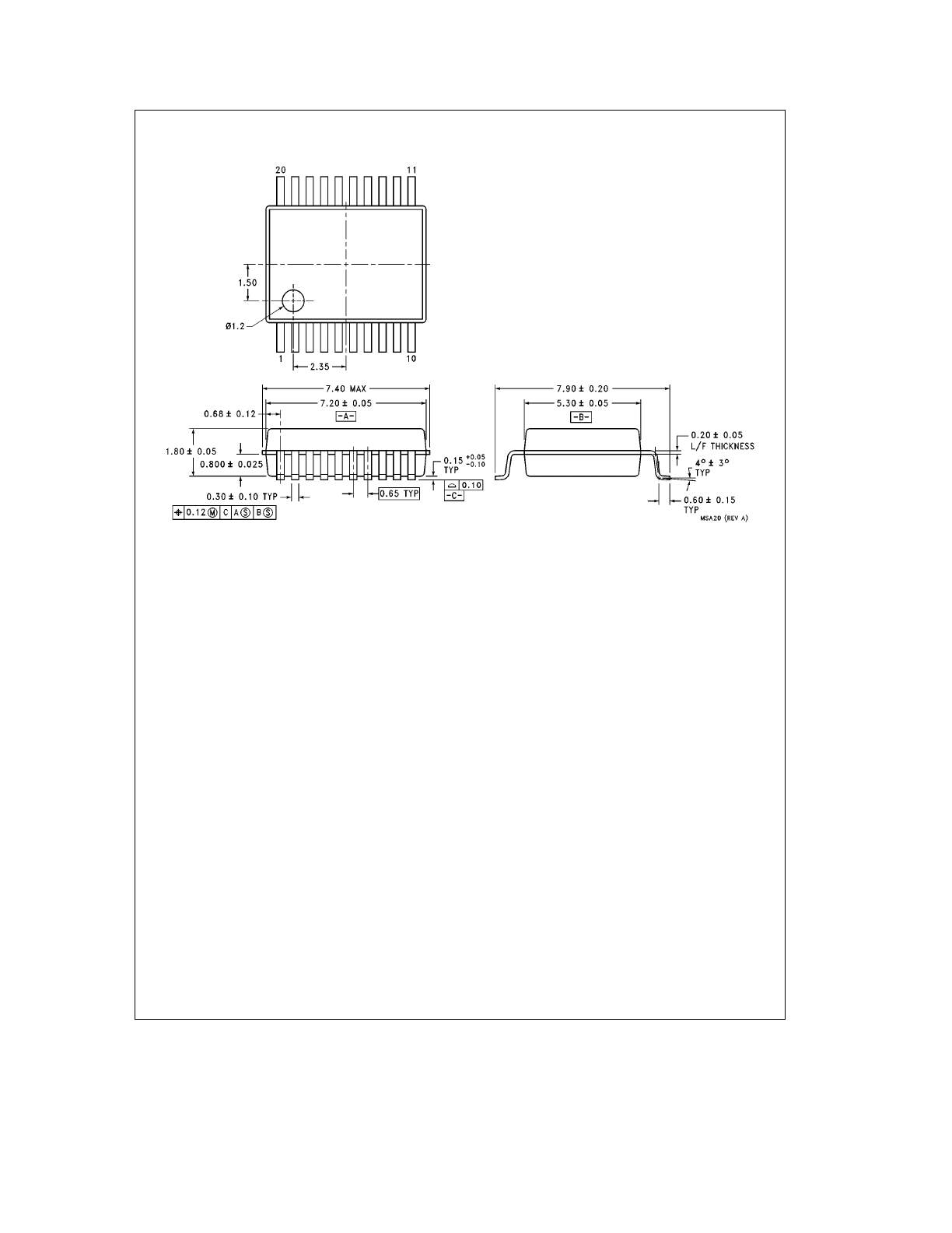
Physical Dimensions
All dimensions are in millimeters (Continued)
20-Lead Molded Shrink Small Outline Package, EIAJ, Type II
Order Number 74LCX573MSA or 74LCX573MSAX
NS Package Number MSA20
7
74LCX573
Low
Voltage
Octal
Latch
with
5V
Tolerant
Inputs
and
Outputs
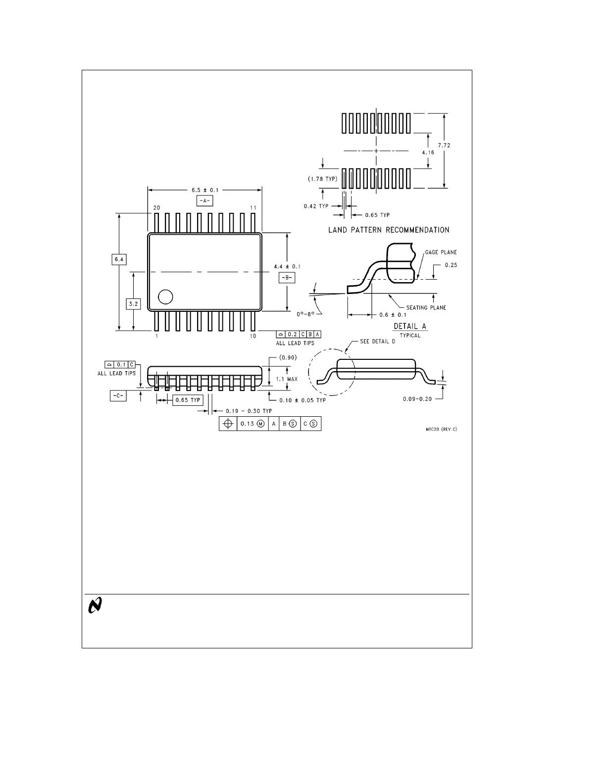
Physical Dimensions
All dimensions are in millimeters (Continued)
20-Lead Think Shrink Small Outline Package, JEDEC
Order Number 74LCX573MTC or 74LCX573MTCX
NS Package Number MTC20
LIFE SUPPORT POLICY
NATIONAL’S PRODUCTS ARE NOT AUTHORIZED FOR USE AS CRITICAL COMPONENTS IN LIFE SUPPORT
DEVICES OR SYSTEMS WITHOUT THE EXPRESS WRITTEN APPROVAL OF THE PRESIDENT OF NATIONAL
SEMICONDUCTOR CORPORATION. As used herein:
1. Life support devices or systems are devices or
2. A critical component is any component of a life
systems which, (a) are intended for surgical implant
support device or system whose failure to perform can
into the body, or (b) support or sustain life, and whose
be reasonably expected to cause the failure of the life
failure to perform, when properly used in accordance
support device or system, or to affect its safety or
with instructions for use provided in the labeling, can
effectiveness.
be reasonably expected to result in a significant injury
to the user.
National Semiconductor
National Semiconductor
National Semiconductor
National Semiconductor
Corporation
Europe
Hong Kong Ltd.
Japan Ltd.
1111 West Bardin Road
Fax: (
a
49) 0-180-530 85 86
13th Floor, Straight Block,
Tel: 81-043-299-2309
Arlington, TX 76017
Email: cnjwge
@
tevm2.nsc.com
Ocean Centre, 5 Canton Rd.
Fax: 81-043-299-2408
Tel: 1(800) 272-9959
Deutsch Tel: (
a
49) 0-180-530 85 85
Tsimshatsui, Kowloon
Fax: 1(800) 737-7018
English
Tel: (
a
49) 0-180-532 78 32
Hong Kong
Fran
3ais Tel: (
a
49) 0-180-532 93 58
Tel: (852) 2737-1600
Italiano
Tel: (
a
49) 0-180-534 16 80
Fax: (852) 2736-9960
National does not assume any responsibility for use of any circuitry described, no circuit patent licenses are implied and National reserves the right at any time without notice to change said circuitry and specifications.