

2010 - 2015 Microchip Technology Inc.
DS00001931A-page 1
General Description
The Microchip USB2660/USB2660i is a USB 2.0 com-
pliant, Hi-Speed hub, card reader, and protocol con-
verter combo solution. This fully integrated single chip
solution provides USB expansion and flash card media
reader/writer integration. The Microchip USB2660/
USB2660i provides an ultra fast interface between a
USB host and today’s popular flash media formats. The
controller allows read/write capability to flash media
from the following families:
- Secure Digital
TM
(SD)
- MultiMediaCard
TM
(MMC)
- Memory Stick
®
(MS)
- xD-Picture Card
TM
(xD)
1
The USB2660/USB2660i offers a versatile, cost-effec-
tive, and energy-efficient hub controller with 2 down-
stream USB 2.0 ports. This combo solution leverages
Microchip’s innovative technology that delivers indus-
try-leading data throughput in mixed-speed USB envi-
ronments. Average sustained transfer rates exceeding
35 MB/s are possible
2
.
Highlights
• 2 exposed Hi-Speed USB 2.0 downstream ports
for external peripheral expansion
• The dedicated flash media reader is internally
attached to a 3rd downstream port of the hub as a
USB Compound Device
- a single or multiplexed flash media reader
interface
- a non-multiplexed SD interface (slot) for SD
card reader
• PortMap - Flexible port mapping and port disable
sequencing supports multiple platform designs
• PortSwap - Programmable USB differential-pair
pin locations eases PCB design by aligning USB
signal traces directly to connectors
• PHYBoost - Programmable USB transceiver
drive strength recovers signal integrity
Features
• Compliance with the following flash media card
specifications SD 2.0 / MMC 4.2 / MS 1.43 / MS-
Pro 1.02 / MS-Pro-HG 1.01 / MS-Duo 1.10 / xD
1.2
• Supports a single external 3.3 V supply source;
internal regulators provide 1.8 V internal core volt-
age for additional bill of materials and power sav-
ings
• The transaction translator (TT) in the hub sup-
ports operation of Full-Speed and Low-Speed
peripherals
• 9 K RAM | 64 K on-chip ROM
• Enhanced EMI rejection and ESD protection per-
formance
• Hub and flash media reader/writer configuration
from a single source: External I
2
C
®
ROM or exter-
nal SPI ROM
- Configures internal code using an external
I
2
C EEPROM
- Supports external code using an SPI Flash
EEPROM
- Customizable vendor ID, product ID, and lan-
guage ID if using an external EEPROM
• Additional SD port for card reader
• The USB2660 supports the commercial tempera-
ture range of 0°C to +70°C
• The USB2660i supports the industrial tempera-
ture range of -40°C to +85°C
• 64-pin QFN RoHS compliant package (9 x 9 mm)
Applications
• Desktop and mobile PCs
• Printers
• GPS navigation systems
• Media players/viewers
• Consumer A/V
• Set-top boxes
• Industrial products
1. For xD-Picture Card
TM
support, please obtain a user
license from the xD-Picture Card License Office.
2. Host and media dependent.
USB2660/USB2660i
Ultra Fast USB 2.0 Hub and Multi-Format Flash Media Controller
with Dual SD Interfaces

USB2660/USB2660i
DS00001931A-page 2
2010 - 2015 Microchip Technology Inc.
TO OUR VALUED CUSTOMERS
It is our intention to provide our valued customers with the best documentation possible to ensure successful use of your Microchip
products. To this end, we will continue to improve our publications to better suit your needs. Our publications will be refined and
enhanced as new volumes and updates are introduced.
If you have any questions or comments regarding this publication, please contact the Marketing Communications Department via
E-mail at
docerrors@microchip.com
. We welcome your feedback.
Most Current Data Sheet
To obtain the most up-to-date version of this data sheet, please register at our Worldwide Web site at:
http://www.microchip.com
You can determine the version of a data sheet by examining its literature number found on the bottom outside corner of any page.
The last character of the literature number is the version number, (e.g., DS30000000A is version A of document DS30000000).
Errata
An errata sheet, describing minor operational differences from the data sheet and recommended workarounds, may exist for cur-
rent devices. As device/documentation issues become known to us, we will publish an errata sheet. The errata will specify the
revision of silicon and revision of document to which it applies.
To determine if an errata sheet exists for a particular device, please check with one of the following:
• Microchip’s Worldwide Web site;
http://www.microchip.com
• Your local Microchip sales office (see last page)
When contacting a sales office, please specify which device, revision of silicon and data sheet (include -literature number) you are
using.
Customer Notification System
Register on our web site at
www.microchip.com
to receive the most current information on all of our products.

2010 - 2015 Microchip Technology Inc.
DS00001931A-page 3
USB2660/USB2660i
Table of Contents
1.0 Overview ......................................................................................................................................................................................... 4
2.0 Block Diagram ................................................................................................................................................................................. 6
3.0 Pin Configuration ............................................................................................................................................................................ 7
4.0 Pin Descriptions .............................................................................................................................................................................. 9
5.0 Pin Reset States ........................................................................................................................................................................... 19
6.0 Configuration Options ................................................................................................................................................................... 22
7.0 AC Specifications .......................................................................................................................................................................... 45
8.0 DC Parameters ............................................................................................................................................................................. 47
9.0 Package Specifications ................................................................................................................................................................. 52
Appendix A: Acronyms ........................................................................................................................................................................ 55
Appendix B: Data Sheet Revision History ........................................................................................................................................... 56
Product Identification System ............................................................................................................................................................. 57
The Microchip Web Site ...................................................................................................................................................................... 59
Customer Change Notification Service ............................................................................................................................................... 59
Customer Support ............................................................................................................................................................................... 59
USB2660/USB2660i
DS00001931A-page 4
2010 - 2015 Microchip Technology Inc.
1.0
OVERVIEW
The Microchip USB2660/USB2660i is an integrated USB 2.0 compliant, Hi-Speed hub, card reader, and protocol con-
verter combo solution. This combo solution supports today’s popular multi-format flash media cards. This multi-format
flash media controller and USB hub combo features two exposed downstream USB ports available for external periph-
eral expansion. The dedicated flash media reader/writer is internally attached to a third downstream port of the hub as
a USB Compound Device which supports the following two interfaces: One interface is multiplexed for xD-Picture Card,
Memory Stick, Secure Digital/MultiMediaCard, and SD/Secure Digital Input/Output. The other interface is dedicated to
a second SD card slot.
The USB2660/USB2660i will attach to an upstream port as a Full-Speed hub or as a Full-/Hi-Speed hub. The hub sup-
ports Low-Speed, Full-Speed, and Hi-Speed (if operating as a Hi-Speed hub) downstream devices on all of the enabled
downstream ports.
All required resistors on the USB ports are integrated into the hub. This includes all series termination resistors on D+
and D– pins and all required pull-down and pull-up resistors. The over-current sense inputs for the downstream facing
ports have internal pull-up resistors.
The USB2660/USB2660i includes programmable features such as:
PortMap which provides flexible port mapping and disable sequences. The downstream ports of a USB2660/USB2660i
hub can be reordered or disabled in any sequence to support multiple platform designs with minimum effort. For any
port that is disabled, the USB2660/USB2660i automatically reorders the remaining ports to match the USB host con-
troller’s port numbering scheme.
PortSwap which adds per-port programmability to USB differential-pair pin locations.
PortSwap allows direct alignment of USB signals (D+/D-) to connectors avoiding
uneven trace length or crossing of the USB differential signals on the PCB.
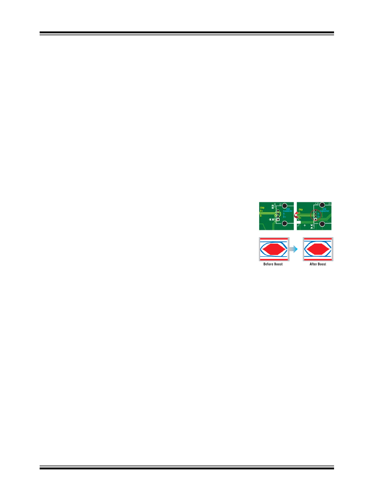
PHYBoost which enables four programmable levels of USB signal drive strengths in
downstream port transceivers. PHYBoost attempts to restore USB signal integrity. The
diagram on the right shows an example of Hi-Speed USB eye diagrams before (PHY-
Boost at 0%) and after (PHYBoost at 12%) signal integrity restoration in a compro-
mised system environment.
1.1
Hardware Features
• Single chip hub and flash media controller combo
• USB2660 supports the commercial temperature range of 0°C to +70°C
• USB2660i supports the industrial temperature range of -40°C to +85°C
• Transaction translator (TT) in the hub supports operation of FS and LS peripherals
• Full power management with individual or ganged power control of each downstream port
• Optional support for external firmware access via SPI interface
• Onboard 24 MHz crystal driver circuit
• Optional external 24 MHz clock input which must be a 1.8 V signal
• Code execution via SPI ROM which must meet
- 30 MHz or 60 MHz operation support
- Single bit or dual bit mode support
- Mode 0 or mode 3 SPI support
1.1.1
COMPLIANCE WITH THE FOLLOWING FLASH MEDIA CARD SPECIFICATIONS:
• Secure Digital 2.0 / MultiMediaCard 4.2
- SD 2.0, SD-HS, SD-HC
- TransFlash™ and reduced form factor media
- 1/4/8 bit MMC 4.2
• Memory Stick 1.43
• Memory Stick Pro Format 1.02

2010 - 2015 Microchip Technology Inc.
DS00001931A-page 5
USB2660/USB2660i
• Memory Stick Pro-HG Duo Format 1.01
- Memory Stick, MS Duo, MS-HS, MS Pro-HG, MS Pro
• Memory Stick Duo 1.10
• xD-Picture Card 1.2
• 8051 8-bit microprocessor
- 60 MHz - single cycle execution
- 64 KB ROM | 9 KB RAM
• Integrated regulator for 1.8 V core operation
1.2
Software Features
• Hub and flash media reader/writer configuration from a single source:
External I
2
C ROM or external SPI ROM
• If the OEM is using an external EEPROM or an external SPI ROM, the following features are available:
- Customizable vendor ID, product ID, and device ID
- 12-hex digits maximum for the serial number string
- 28-character manufacturer ID and product strings for the flash media reader/writer
1.3
OEM Selectable Hub Features
A default configuration is available in the USB2660/USB2660i following a reset. The USB2660/USB2660i may also be
configured by an external I
2
C EEPROM or via external SPI ROM flash.
• Compound Device support on a port-by-port basis
- a port is permanently hardwired to a downstream USB peripheral device
• Select over-current sensing and port power control on an individual or ganged (all ports together) basis to match
the OEM’s choice of circuit board component selection
• Port power control and over-current detection/delay features
• Configure the delay time for filtering the over-current sense inputs
• Configure the delay time for turning on downstream port power
• Bus- or self-powered selection
• Hub port disable or non-removable configurations
• Flexible port mapping and disable sequencing supports multiple platform designs
• Programmable USB differential-pair pin location eases PCB layout by aligning USB signal lines directly to connec-
tors
• Programmable USB signal drive strength recovers USB signal integrity using 4 levels of signal drive strength
• Indicate the maximum current that the 2-port hub consumes from the USB upstream port
• Indicate the maximum current required for the hub controller
USB2660/USB2660i
DS00001931A-page 6
2010 - 2015 Microchip Technology Inc.
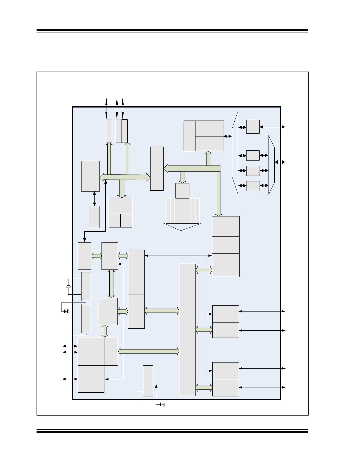
2.0
BLOCK DIAGRAM
FIGURE 2-1:
USB2660/USB2660I BLOCK DIAGRAM
To
Upstream
V
BUS
U
p
st
re
am
PHY
Up
st
ream
USB
Dat
a
Re
pea
ter
Cont
ro
ll
e
r
Se
ri
a
l
In
te
rf
ac
e
En
g
in
e
Se
ri
a
l
In
te
rfa
c
e
R
out
ing & Por
t
Re-
O
rder
ing
Logi
c
P
o
rt
Cont
ro
ll
e
r
PHY
Po
rt
#
3
OC
Se
n
s
e
Swi
tc
h
Dr
iver
Bu
s
-P
o
w
e
r
Det
e
c
t/
V
BUS
P
u
ls
e
T
ra
n
sa
ct
io
n
T
ran
s
lat
o
r
PHY
Po
rt #2
OC
Sen
s
e
Sw
itc
h
Dri
v
e
r
USB Data
D
o
w
n
stream
OC
S
e
nse
/
Pw
r Sw
it
c
h
80
51
P
R
OC
ES
SO
R
SFR
RA
M
XDATA BRI
DG
E
+ BU
S
ARBI
TER
64
K
ROM
RAM
6 K
AD
DR
MAP
Progr
am
Me
m
o
ry
I
/O Bus
P
W
R_FET0
3 K
to
tal
RAM
BUS
IN
TFC
EP
0 T
X
EP
0 R
X
SIE
CTL
BR
ID
G
E
BUS
IN
TFC
FMDU
CTL
AU
TO
_
CBW
PR
O
C
FM
I
BUS
IN
TFC
USB Data
D
o
w
n
str
e
am
MS
OC
S
e
nse
/
Pw
r S
w
it
c
h
3.
3 V
1.8 V
PLL
24 M
H
z
C
ryst
al
1.
8 V
R
e
g
3.
3 V
1.
8
V
R
e
g
VDDCR
SD/
MM
C
/
SDI
O
SD
/
MM
C
F
lash
M
e
di
a C
a
rd
s
(requ
ir
e
com
bo s
o
cket
)
S
D
/M
M
C
S
o
cket
o
r
S
D
IO
In
te
rco
nne
ct
EP2 RX
EP
2 T
X
SP
I
SPI
(
4
pi
n
s
)
PW
R_FET1
CR
D_PW
R2
xD
*
*F
o
r x
D
-P
ic
tu
re
C
a
rd
TM
s
u
pp
or
t,
pl
eas
e
ob
ta
in
a
u
s
er
lic
e
n
s
e
f
ro
m
th
e
x
D
-P
ic
tu
re
C
a
rd
L
ic
e
n
s
e
O
ffic
e
.
C
RD_PW
R1
2010 - 2015 Microchip Technology Inc.
DS00001931A-page 7
USB2660/USB2660i
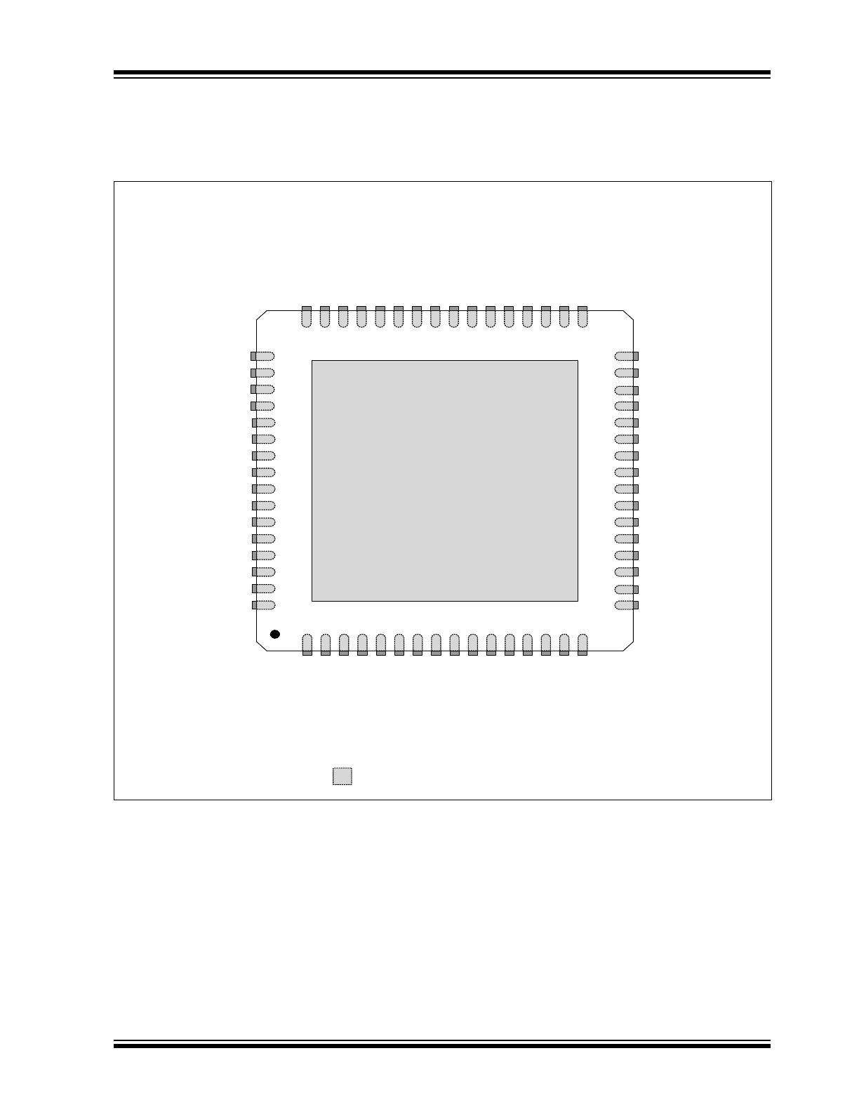
3.0
PIN CONFIGURATION
FIGURE 3-1:
USB2660/USB2660I 64-PIN QFN
Ground Pad
(must be connected to VSS)
USB2660/USB2660i
(Top View QFN-64)
Indicates pins on the bottom of the device.
nRESET
54
VBUS_DET
55
LED / TXD
53
TEST
56
VDD33
57
USBUP_DM
59
XTAL2
60
XTAL1 (CLKIN)
61
RBIAS
64
VDD33
63
PLLFILT
62
USBUP_DP
58
VDD3
3
1
USB
D
N_
DM2
2
US
BDN_DP
2
3
USB
D
N_
DM3
4
US
BDN_DP
3
5
PR
T
C
T
L
2
6
PR
T
C
T
L
3
7
SD
2
_
W
P
8
SD2_
nCD
9
10
SD2_
D0
11
SD2_
D1
12
21
SD1_CLK / MS_BS / xD_nW P
20
SD1_D6 / MS_D7 / xD_D0
19
SD1_D7 / MS_D6 / xD_D1
18
SD1_D0 / MS_D4 / xD_D2
17
CRFILT
SD1_D1 / MS_D5 / xD_D3
VDD33
SD1_nCD
SD1_W P / MS_SCLK / xD_D4
23
SD1_D5 / MS_D1 / xD_ALE
22
xD_nW E
24
SD1_CMD / MS_D0 / xD_CLE
43
NC
42
CR
D_
P
W
R
1
41
V
DD33
40
S
D
1_
D3 / MS_
D
3 / xD
_
D
6
39
MS
_
IN
S
38
S
D
1_
D4 / MS_
D
2 / xD
_
D
7
37
xD_
n
C
D
36
xD_
n
B/
R
44
S
D
1_
D2 / xD_D5
35
xD_
n
R
E
34
xD_
n
C
E
33
V
DD33
SD2_
D7
SD2_
D6
S
D
2_CL
K
SD2_
D5
13
14
15
16
32
31
30
29
28
27
26
25
47
46
CRD_P
W
R2
45
48
50
51
49
52
SPI_CE_n
SPI_CLK / SCL
SPI_DI
SPI_DO / SDA / SPI_SPD_SEL
SD2_D2
SD2_D3
SD2_D4
SD2_CMD
VDD3
3
NC
V
DD33
NC
USB2660/USB2660i
DS00001931A-page 8
2010 - 2015 Microchip Technology Inc.
3.1
64-Pin Table
TABLE 3-1:
USB2660/USB2660I 64-PIN TABLE
SECURE DIGITAL / MEMORY STICK / xD INTERFACE (18 PINS)
SD1_D7 /
MS_D6 /
xD_D1
SD1_D6 /
MS_D7 /
xD_D0
SD1_D5 /
MS_D1 /
xD_ALE
SD1_D4 /
MS_D2 /
xD_D7
SD1_D3 /
MS_D3 /
xD_D6
SD1_D2 /
xD_D5
SD1_D1 /
MS_D5 /
xD_D3
SD1_D0 /
MS_D4 /
xD_D2
SD1_CLK /
MS_BS /
xD_ nWP
SD1_CMD /
MS_D0 /
xD_CLE
SD1_nCD
MS_INS
SD1_WP /
MS_SCLK /
xD_D4
xD_nCD
xD_nB/R
xD_nRE
xD_nCE
xD_nWE
SECOND SECURE DIGITAL INTERFACE (12 PINS)
SD2_D7
SD2_D6
SD2_D5
SD2_D4
SD2_D3
SD2_D2
SD2_D1
SD2_D0
SD2_NCD
SD2_CLK
SD2_CMD
SD2_W
USB INTERFACE (5 PINS)
USBUP_DP
USBUP_DM
XTAL1 (CLKIN)
XTAL2
RBIAS
2-PORT USB INTERFACE (7 PINS)
USBDN_DP2
USBDN_DM2
PRTCTL2
PRTCTL3
USBDN_DP3
USBDN_DM3
VBUS_DET
SPI INTERFACE (4 PINS)
SPI_CE_n
SPI_CLK /
SCL
SPI_DO /
SDA /
SPI_SPD_SEL
SPI_DI
MISC (8 PINS)
nRESET
TEST
LED
CRD_PWR2
CRD_PWR1
(3) NC
POWER (10 PINS)
(8) VDD33
CRFILT
PLLFILT
TOTAL 64
2010 - 2015 Microchip Technology Inc.
DS00001931A-page 9
USB2660/USB2660i
4.0
PIN DESCRIPTIONS
This section provides a detailed description of each signal. The signals are arranged in functional groups according to
their associated interface. The pin descriptions below are applied when using the internal default firmware and can be
referenced in
Section 6.0, "Configuration Options," on page 22
. Please reference
Section Appendix A:, "Acronyms," on
page 55
for a list of the acronyms used.
The “n” symbol in the signal name indicates that the active, or asserted, state occurs when the signal is at a low voltage
level. When “n” is not present in the signal name, the signal is asserted at a high voltage level.
The terms assertion and negation are used exclusively. This is done to avoid confusion when working with a mixture of
“active low” and “active high” signals. The term assert, or assertion, indicates that a signal is active, independent of
whether that level is represented by a high or low voltage. The term negate, or negation, indicates that a signal is inac-
tive.
4.1
USB2660/USB2660i Pin Descriptions
TABLE 4-1:
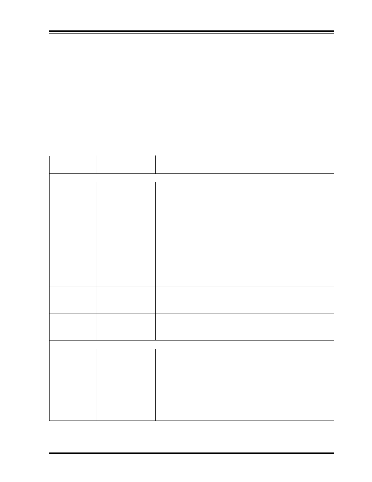
USB2660/USB2660I PIN DESCRIPTIONS
Symbol
64-PIN
QFN
Buffer Type
(
Table 4-2
)
Description
SECURE DIGITAL INTERFACE
SD1_D[7:0]
27
28
31
38
40
41
25
26
I/O8PU
Secure Digital Data 7-0
These are the bi-directional data signals SD_D0 - SD_D7 with weak
pull-up resistors.
SD1_CLK
29
O8
Secure Digital Clock
This is an output clock signal to the SD/MMC device.
SD1_CMD
32
I/O8PU
Secure Digital Command
This is a bi-directional signal that connects to the CMD signal of the
SD/MMC device. The bi-directional signal has a weak internal pull-up
resistor.
SD1_nCD
22
I/O8PU
Secure Digital Card Detect
Designates as the Secure Digital card detection pin and has an internal
pull-up.
SD1_WP
21
I/O8
Secure Digital Write Protected
Designates as the Secure Digital card mechanical write protect detect
pin.
SECOND SECURE DIGITAL INTERFACE
SD2_D[7:0]
11
12
16
18
19
20
9
10
I/O8PU
SD2 Data 7-0
These are the bi-directional data signals SD2_D0 - SD2_D7 and have
weak pull-up resistors.
SD2_CLK
13
O8
SD2 Clock
This is an output clock signal designated for to the SD2/MMC device.

USB2660/USB2660i
DS00001931A-page 10
2010 - 2015 Microchip Technology Inc.
SD2_CMD
17
I/O8PU
SD2 Command
This is a bi-directional signal designated by for the CMD signal of the
SD2/MMC device. The bi-directional signal has a weak internal pull-up
resistor.
SD2_nCD
8
I/O8
SD2 Card Detect
Designates as the second Secure Digital card detection pin and has an
internal pull-up.
SD2_WP
45
I/O8
SD2 Write Protected
Designates as the second Secure Digital card interface mechanical
write detect pin.
MEMORY STICK INTERFACE
MS_BS
29
O8
Memory Stick Bus State
This pin is connected to the bus state pin of the MS device. It is used
to control the Bus States 0, 1, 2, and 3 (BS0, BS1, and BS3) of the MS
device.
MS_INS
39
IPU
Memory Stick Card Insertion
Designates as the Memory Stick card detection pin and has a weak
internal pull-up resistor.
MS_SCLK
21
O8
Memory Stick System Clock
This pin is an output clock signal to the MS device.
MS_D[7:0]
28
27
25
26
40
38
31
32
I/O8PD
Memory Stick System Data In/Out
These pins are the bi-directional data signals for the MS device. In serial
mode, the most significant bit (MSB) of each byte is transmitted first by
either MSC or MS device on MS_D0.
MS_D0, MS_D2, and MS_D3 have weak pull-down resistors. MS_D1
has a pull-down resistor if in parallel mode, otherwise it is disabled. In
4- or 8-bit parallel modes, all MS_D7 - MS_D0 signals have weak pull-
down resistors.
xD-PICTURE CARD INTERFACE
xD_D[7:0]
38
40
41
21
25
26
27
28
I/O8PD
xD-Picture Card Data 7-0
These pins are the bi-directional data signals xD_D7 - xD_D0 and have
weak internal pull-down resistors.
xD_ALE
31
O8PD
xD-Picture Card Address Strobe
This pin is an active high Address Latch Enable (ALE) signal for the xD
device. This pin has a weak pull-down resistor that is permanently
enabled.
TABLE 4-1:
USB2660/USB2660I PIN DESCRIPTIONS (CONTINUED)
Symbol
64-PIN
QFN
Buffer Type
(
Table 4-2
)
Description