

2014 Microchip Technology Inc.
DS00001760B-page 1
Highlights
• Integrated USB Power Delivery (PD) PHY
• Support for Power Delivery Message Protocol
• Integrated Voltage and Current ADC Inputs
• Configuration Profile Selection
• On-chip Microcontroller
• SPI Interface
• Commercial and Industrial Grade Temperature
Support
• Available in 32-SQFN Package
Target Applications
• Notebooks
• Ultrabooks
• Desktop PCs
• Docking Stations
• Monitors
• Printers
Key Benefits
• Integrated USB Power Delivery (PD) PHY
- Integrated receive termination
- Requires minimal external components
• Support for Power Delivery Message Protocol
- Message Generation/Consumption
- Retry Generation
- Error Handling
- State Behavior
• Cable Detect Logic
- Cable attachment type
• CFG_SEL pins allow selection of multiple profiles
- Provider
- Provider/Consumer
- Consumer
- Consumer/Provider
• Integrated Voltage (VMON) and Current (IMON)
ADC Inputs
• Dead Battery Support
• On-chip Microcontroller
- Manages I/Os and other signals
- Implements power delivery policy engine and
device policy manager
• Configuration Programming via OTP, or Vendor
Defined Messaging
• Supports Low Power Modes
• Serial Peripheral Interface (SPI) Bus
• Internal 3.3 V and 1.8 V Voltage Regulators
• Integrated Oscillator Reduces BOM Costs
• Package
- 32-pin SQFN (5 x 5 mm)
• Environmental
- Commercial temperature range (0°C to +70°C)
- Industrial temperature range (-40°C to +85°C
UPD1002
USB Power Delivery Controller

UPD1002
DS00001760B-page 2
2014 Microchip Technology Inc.
TO OUR VALUED CUSTOMERS
It is our intention to provide our valued customers with the best documentation possible to ensure successful use of your Microchip
products. To this end, we will continue to improve our publications to better suit your needs. Our publications will be refined and
enhanced as new volumes and updates are introduced.
If you have any questions or comments regarding this publication, please contact the Marketing Communications Department via
E-mail at
docerrors@microchip.com
. We welcome your feedback.
Most Current Documentation
To obtain the most up-to-date version of this documentation, please register at our Worldwide Web site at:
http://www.microchip.com
You can determine the version of a data sheet by examining its literature number found on the bottom outside corner of any page.
The last character of the literature number is the version number, (e.g., DS30000000A is version A of document DS30000000).
Errata
An errata sheet, describing minor operational differences from the data sheet and recommended workarounds, may exist for cur-
rent devices. As device/documentation issues become known to us, we will publish an errata sheet. The errata will specify the
revision of silicon and revision of document to which it applies.
To determine if an errata sheet exists for a particular device, please check with one of the following:
• Microchip’s Worldwide Web site;
http://www.microchip.com
• Your local Microchip sales office (see last page)
When contacting a sales office, please specify which device, revision of silicon and data sheet (include -literature number) you are
using.
Customer Notification System
Register on our web site at
www.microchip.com
to receive the most current information on all of our products.

2014 Microchip Technology Inc.
DS00001760B-page 3
UPD1002
Table of Contents
1.0 Introduction ..................................................................................................................................................................................... 4
2.0 Pin Descriptions and Configuration ................................................................................................................................................. 7
3.0 Functional Descriptions ................................................................................................................................................................. 23
4.0 Operational Characteristics ........................................................................................................................................................... 37
5.0 Package Outline ............................................................................................................................................................................ 41
6.0 Revision History ............................................................................................................................................................................ 42
The Microchip Web Site ...................................................................................................................................................................... 43
Customer Change Notification Service ............................................................................................................................................... 43
Customer Support ............................................................................................................................................................................... 43
Product Identification System ............................................................................................................................................................. 44

UPD1002
DS00001760B-page 4
2014 Microchip Technology Inc.
1.0
INTRODUCTION
1.1
General Description
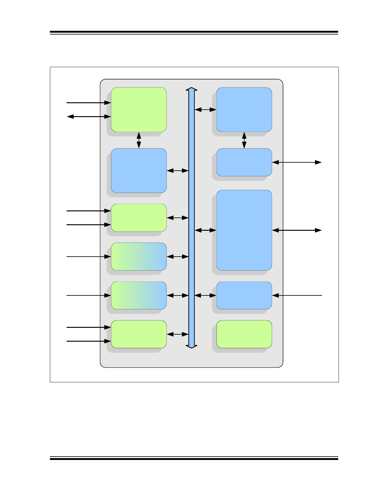
The UPD1002 is a USB Power Delivery (PD) controller designed to adhere to the USB Power Delivery Specification.
USB Power Delivery allows a host (or device) to provide or consume up to 5 Amps and/or up to 20 Volts of power from
a USB PD capable partner device on the other end of the USB cable. USB PD capable standard and custom cables/
connectors are supported, which in most cases are backward compatible with standard USB connections.
The UPD1002 provides a complete USB Power Delivery solution for notebooks/ultrabooks, desktop PCs, monitors, and
docking stations, (see
Table 1-1, “UPD1002 Package/Pin Configuration Summary,” on page 6
for available configura-
tions and corresponding applications). The functionality of the UPD1002 is selected via two configuration selection pins,
CFG_SEL0 and CFG_SEL1, which can be used to select unique PD and system configurations. Designing the
UPD1002 into a system can be as simple as selecting a configuration, with no external EEPROM required. Advanced
programmability options exist with an external EEPROM installed.
The integrated USB Power Delivery MAC and PHY support provider and consumer operation via the PD communication
protocol, as specified in Revision 1.0 (Version 1.2) of the USB Power Delivery Specification. Monitoring of VBUS and
battery charging is accomplished via the integrated voltage and current ADC inputs. The PHY supports cable ID detec-
tion/identification and loopback modes. The PHY includes a 24MHz FSK modulator/demodulator and provides inte-
grated terminations. The USB PD MAC supports both USB PD insertion detection (cold socket) and dead battery cases.
The device provides an integrated voltage switch which is used to detect whether the VBUS or VTR (battery) power
supply is active, enabling selection of the appropriate power supply at any given time.
The on-chip microcontroller manages the IOs and implements the power delivery local policy engine and device man-
ager. The SPI ROM controller is used by the microcontroller for optional external code execution from ROM. A One Time
Programmable (OTP) ROM is integrated in the UPD1002. Integrated 3.3 V and 1.8 V regulators allow device operation
from a single power supply. The UPD1002 is available in commercial (0°C to +70°C) and industrial (-40°C to +85°C)
temperature ranges. An internal block diagram of the UPD1002 is shown in
Figure 1-1
.
Power Delivery applications introduce two different types of USB ports. The Upstream Facing Port (UFP) and the Down-
stream Facing Port (DFP). The UFP and DFP have different usages and attributes due to the nature of their use cases,
as detailed below. For a list of available UPD1002 configurations and corresponding target applications, refer to
Table 1-
1, “UPD1002 Package/Pin Configuration Summary,” on page 6
.
The Upstream Facing Port (UFP)
The primary use case of the UFP is to connect to a host computer. In this case, the UFP of the UPD1002 must have a
Standard-B (STD-B) USB connector to connect to the host’s Standard-A (STD-A) USB connector. If the host is a note-
book/ultrabook, it may request to be charged from the UPD1002 UFP, requiring the system to be wall powered instead
of bus-powered. In this case, the UFP must offer a Consumer/Provider role.
The Downstream Facing Port (DFP)
The primary use case of the DFP is to connect to other downstream USB devices such as speakers, keyboard, mice,
scanners, external hard drives, external optical drives, printers, etcetera. These devices are mainly Consumers in
nature in the first phase of adoption. DFPs are Providers by default and have Standard-A USB connectors. Battery
Charging 1.2 support can be provided by a parallel USB hub or a Microchip UCS100x or other enhanced port power
controller device.
2014 Microchip Technology Inc.
DS00001760B-page 5
UPD1002
FIGURE 1-1:
INTERNAL BLOCK DIAGRAM
Power
Delivery
AFE
Power
Delivery
MAC
PD_DATA
PD_ID
Configuration
Select
CFG_SEL0
CFG_SEL1
Voltage
Monitor
VMON
Clocks
Micro-
controller
SPI ROM
Controller
Current
Monitor
IMON
SPI ROM
I/O
Controller
†
I/O
†
Specific I/O functions are determined by package and CFG_SEL0/CFG_SEL1 profile selection.
RESET_N
Reset
Controller
Voltage
Switch
VBUS
VTR
UPD1002

UPD1002
DS00001760B-page 6
2014 Microchip Technology Inc.
The UPD1002 is offered in a 32-pin SQFN package. The package provides multiple pin configurations, based upon the
CFG_SEL0 and CFG_SEL1 Configuration Select signals.
Table 1-1
summarizes the available pin combinations and
their target applications. Refer to
Section 2.0, "Pin Descriptions and Configuration," on page 7
for detailed information
on specific pin configurations.
TABLE 1-1:
UPD1002 PACKAGE/PIN CONFIGURATION SUMMARY
Package
Pin Config.
Name
DFP/
UFP
PD Role
USB
Receptacle Target
Applications
Notes
32-SQFN
32-P_A DFP
Provider
Standard-A
(STD-A)
• Monitors
• Docking stations
• Desktop PCs
• Printers
See
Section 2.1
32-CP_B UFP
Consumer/Provider Standard-B
(STD-B)
• Monitors
• Docking stations
• Printers
See
Section 2.1
32-PC_A DFP
Provider/Consumer Standard-A
(STD-A)
• Notebooks
See
Section 2.1
No VSELx_N
32-PC_uAB DFP
Provider/Consumer Micro-AB
(uAB)
• Notebooks
• Ultrabooks
See
Section 2.1
No VSELx_N
2014 Microchip Technology Inc.
DS00001760B-page 7
UPD1002
2.0
PIN DESCRIPTIONS AND CONFIGURATION
The pinouts for the package, along with system-level application diagrams, are detailed in the following section:
•
32-Pin SQFN (32-SQFN)
Note:
For a summary of the available pin combinations and their corresponding target applications, refer to
Table 1-1
.
Pin descriptions are detailed in
Section 2.2, "Pin Descriptions," on page 14
. For details on the CFG_SEL0 and CFG_-
SEL1 Configuration Select signals, refer to
Section 3.3, "Configuration Selection (CFG_SEL0/CFG_SEL1)," on
page 24
.
2.1
32-Pin SQFN (32-SQFN)
2.1.1
32-SQFN PIN DIAGRAM
Note:
When an “_N” is used at the end of the signal name, it indicates that the signal is active low. For example,
RESET_N indicates that the reset signal is active low.
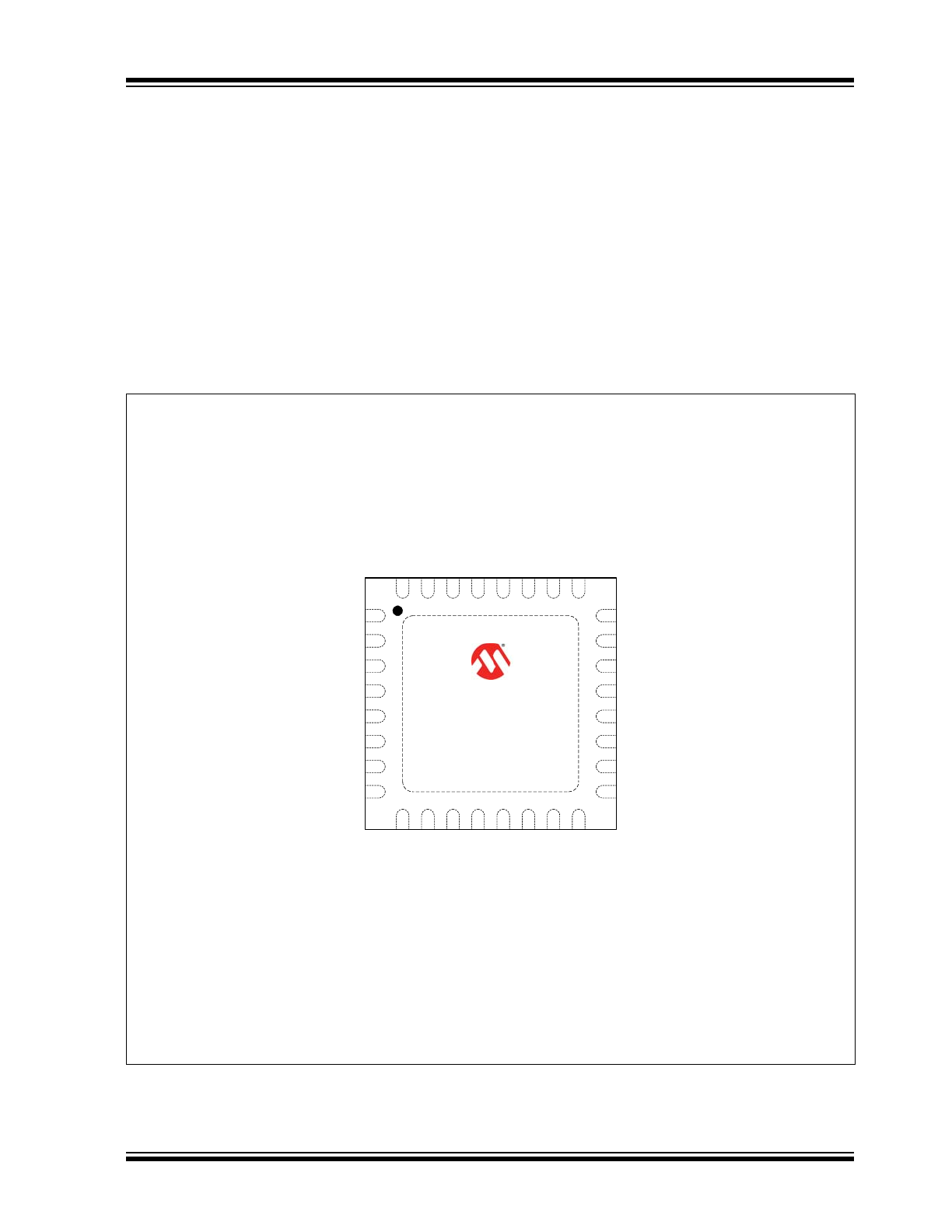
FIGURE 2-1:
32-SQFN PIN ASSIGNMENTS (TOP VIEW)
(Connect exposed pad to ground with a via field)
VSS
UPD1002
32-SQFN
( T o p V i e w )
Note: Exposed pad (VSS) on bottom of package must be connected to ground with a via field.
*The functionality of this pin is dependent on the CFG_SEL0/CFG_SEL1 profile selection.
1
2
3
4
5
6
7
8
9
10
11
12
13
14
15
16
24
23
22
21
20
19
18
17
32
31
30
29
28
27
26
25
CFG_SEL1
CFG_SEL0
PD_EN/PD_GOOD*
VDD33_CAP
VBUS
VSW_CAP
VTR
VDD18A_CAP
PD_DATA
PD_ID
PD_VDD18
VDDIO
IMON
VMON
F
A
U
LT_IN_N
F
A
U
LT_N
CHG
_
EMU_EN
/V
S
A
F
E
DB_
E
N
/
PP
C_P
W
R_EN*
VSE
L
2_N
/V
BUS_OUT/
VBUS_D
IS
CH
ARG
E*
VSE
L
1_N
/U
SB_ID
_
IND
/N
C
*
IN
S
E
RTION_D
ETECT/VS
EL0_
N
/N
C
*
V
B
US_
D
IS
CH
AR
GE
/E
X
T
_
P
W
R
_
D
E
T
*
S
P
I_
RO
M
_
DI
S
P
I_
ROM
_
DO
SP
I_
R
O
M_
C
L
K
SP
I_
RO
M_
CE
_
N
TE
S
T
VDD18_CAP
RES
ET_
N
PD_D
ETECT/VS
EL1_
N
/N
C
*
VSE
L
0_N
/V
BUS_OUT/N
C
*
V
DDI
O
HUB_PWR_EN/VSEL2_N*

UPD1002
DS00001760B-page 8
2014 Microchip Technology Inc.
Note:
The buffer type for each signal is indicated in the BUFFER TYPE column of
Table 2-2, "Pin Descriptions"
.
A description of the buffer types is provided in
Section 2.3, "Buffer Types"
.
2.1.2
32-SQFN PIN ASSIGNMENTS
The UPD1002 32-SQFN provides four distinct pin configurations (32-P_A, 32-CP_B, 32-PC_A, and 32-PC_uAB) based
upon the CFG_SEL0 and CFG_SEL1 Configuration Select signals. These configurations are designed for specific appli-
cations, as outlined in
Table 1-1, “UPD1002 Package/Pin Configuration Summary,” on page 6
. The 32-SQFN package
pin assignments for each configuration are detailed in
Table 2-1
. For pin descriptions, refer to
Section 2.2, "Pin Descrip-
tions"
. For example connection diagrams, refer to
Section 2.4, "Power Connection Diagram," on page 22
. For informa-
tion on the Configuration Select signals, refer to
Section 3.3, "Configuration Selection (CFG_SEL0/CFG_SEL1)"
.
TABLE 2-1:
32-SQFN PACKAGE PIN ASSIGNMENTS
Pin
Number
Configuration
32-P_A
Pin Name
Configuration
32-CP_B
Pin Name
Configuration
32-PC_A
Pin Name
Configuration
32-PC_uAB
Pin Name
1
CFG_SEL0
2
CFG_SEL1
3
PD_EN
PD_EN
PD_GOOD
PD_GOOD
4
VDD33_CAP
5
VBUS
6
VSW_CAP
7
VTR
8
VDD18A_CAP
9
SPI_ROM_CE_N
10
SPI_ROM_CLK
11
SPI_ROM_DO
12
SPI_ROM_DI
13
VDDIO
14
VBUS_DISCHARGE
VBUS_DISCHARGE
EXT_PWR_DET
EXT_PWR_DET
15
INSERTION_DETECT
VSEL0_N
INSERTION_DETECT
NC
16
PD_DETECT
VSEL1_N
PD_DETECT
NC
17
VMON
18
IMON
19
VDDIO
20
VDD18_CAP
21
PD_VDD18
22
HUB_PWR_EN
VSEL2_N
HUB_PWR_EN
HUB_PWR_EN
23
PD_ID
24
PD_DATA
25
CHG_EMU_EN
VSAFEDB_EN
PPC_PWR_EN
PPC_PWR_EN
26
TEST
27
RESET_N
2014 Microchip Technology Inc.
DS00001760B-page 9
UPD1002
28
VSEL0_N
NC
NC
VBUS_OUT
29
VSEL1_N
NC
NC
USB_ID_IND
30
FAULT_N
31
FAULT_IN_N
32
VSEL2_N
VBUS_OUT
VBUS_DISCHARGE
VBUS_DISCHARGE
Exposed
Pad
VSS
TABLE 2-1:
32-SQFN PACKAGE PIN ASSIGNMENTS (CONTINUED)
Pin
Number
Configuration
32-P_A
Pin Name
Configuration
32-CP_B
Pin Name
Configuration
32-PC_A
Pin Name
Configuration
32-PC_uAB
Pin Name
UPD1002
DS00001760B-page 10
2014 Microchip Technology Inc.
2.1.3
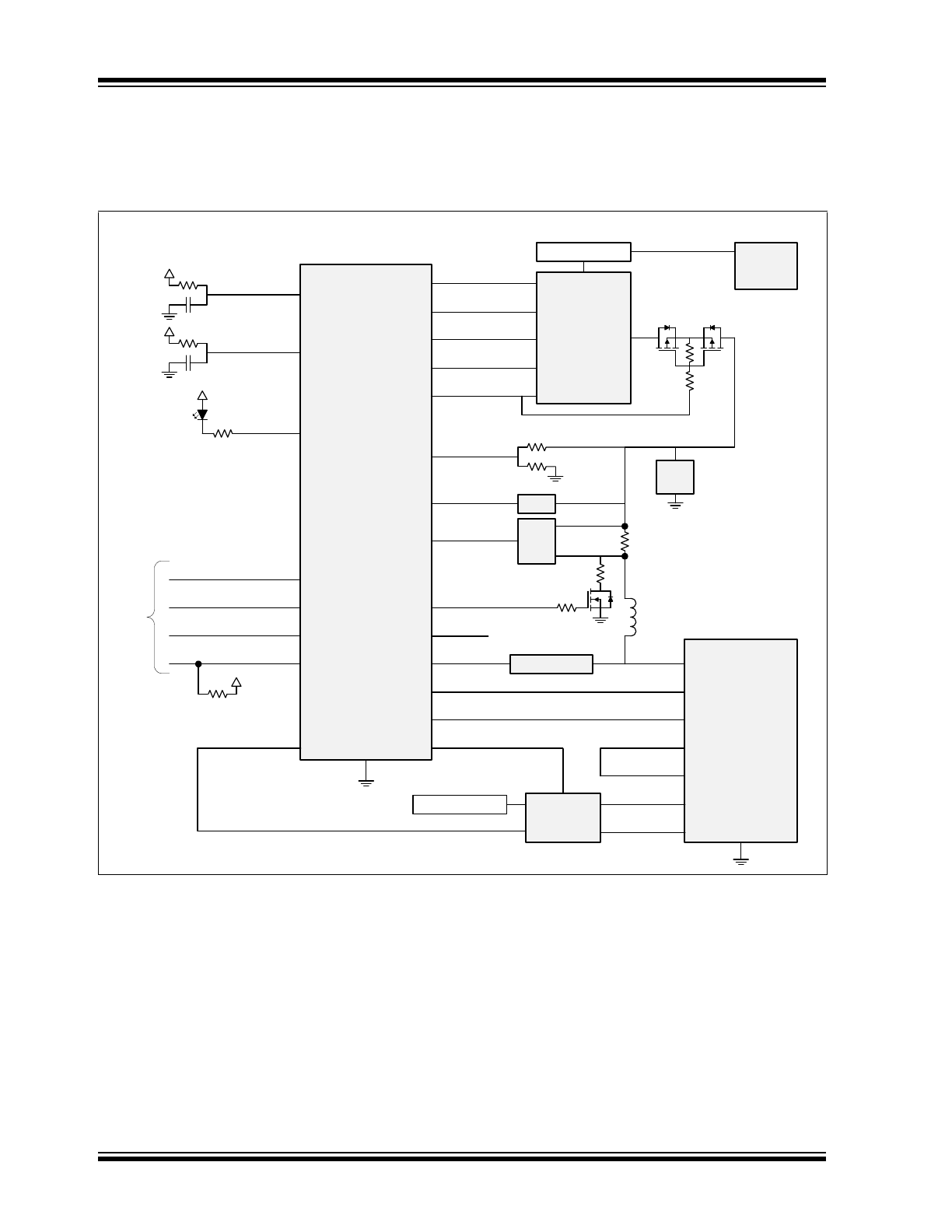
32-SQFN SYSTEM LEVEL DIAGRAMS
Figure 2-2
,
Figure 2-3
,
Figure 2-4
, and
Figure 2-5
provide typical system level diagrams of the UPD1002 for configura-
tions 32-P_A, 32-CP_B, 32-PC_A, and 32-PC_uAB, respectively.
FIGURE 2-2:
CONFIGURATION 32-P_A SYSTEM-LEVEL DIAGRAM
Microchip
UPD1002
32-SQFN
Configuration
32-P_A
SPI_ROM_CLK
SPI_ROM_DI
SPI_ROM_DO
SPI_ROM_CE_N
To SPI
R
O
M
VSS
CFG_SEL0
VDDIO
CFG_SEL1
VDDIO
VDDIO
VMON
IMON
CSA
PD_DETECT 1
PD_ID
VBUS
Couple/Filter
PD_DATA
PD_DETECT
INSERTION_DETECT
INSERTION_DETECT 2
INSERTION_DETECT 1
SHIELD
35.7k
5.1k
HUB_PWR_EN
5V
VBUS
VSEL2_N
PD_EN
USB Hub
with BC1.2
GND
USB
Power
Delivery
Enabled
Standard-A
Receptacle
D+
D-
VSEL1_N
FAULT_IN_N
VSEL0_N
VDDIO
FAULT_N
CHG_EMU_EN
DC-to-DC
Power
Regulator
System Power
Standard
24V AC
Adapter
Filter
Cap
VBUS_DISCHARGE
FAULT_IN_N
2014 Microchip Technology Inc.
DS00001760B-page 1
Highlights
• Integrated USB Power Delivery (PD) PHY
• Support for Power Delivery Message Protocol
• Integrated Voltage and Current ADC Inputs
• Configuration Profile Selection
• On-chip Microcontroller
• SPI Interface
• Commercial and Industrial Grade Temperature
Support
• Available in 32-SQFN Package
Target Applications
• Notebooks
• Ultrabooks
• Desktop PCs
• Docking Stations
• Monitors
• Printers
Key Benefits
• Integrated USB Power Delivery (PD) PHY
- Integrated receive termination
- Requires minimal external components
• Support for Power Delivery Message Protocol
- Message Generation/Consumption
- Retry Generation
- Error Handling
- State Behavior
• Cable Detect Logic
- Cable attachment type
• CFG_SEL pins allow selection of multiple profiles
- Provider
- Provider/Consumer
- Consumer
- Consumer/Provider
• Integrated Voltage (VMON) and Current (IMON)
ADC Inputs
• Dead Battery Support
• On-chip Microcontroller
- Manages I/Os and other signals
- Implements power delivery policy engine and
device policy manager
• Configuration Programming via OTP, or Vendor
Defined Messaging
• Supports Low Power Modes
• Serial Peripheral Interface (SPI) Bus
• Internal 3.3 V and 1.8 V Voltage Regulators
• Integrated Oscillator Reduces BOM Costs
• Package
- 32-pin SQFN (5 x 5 mm)
• Environmental
- Commercial temperature range (0°C to +70°C)
- Industrial temperature range (-40°C to +85°C
UPD1002
USB Power Delivery Controller
UPD1002
DS00001760B-page 2
2014 Microchip Technology Inc.
TO OUR VALUED CUSTOMERS
It is our intention to provide our valued customers with the best documentation possible to ensure successful use of your Microchip
products. To this end, we will continue to improve our publications to better suit your needs. Our publications will be refined and
enhanced as new volumes and updates are introduced.
If you have any questions or comments regarding this publication, please contact the Marketing Communications Department via
E-mail at
docerrors@microchip.com
. We welcome your feedback.
Most Current Documentation
To obtain the most up-to-date version of this documentation, please register at our Worldwide Web site at:
http://www.microchip.com
You can determine the version of a data sheet by examining its literature number found on the bottom outside corner of any page.
The last character of the literature number is the version number, (e.g., DS30000000A is version A of document DS30000000).
Errata
An errata sheet, describing minor operational differences from the data sheet and recommended workarounds, may exist for cur-
rent devices. As device/documentation issues become known to us, we will publish an errata sheet. The errata will specify the
revision of silicon and revision of document to which it applies.
To determine if an errata sheet exists for a particular device, please check with one of the following:
• Microchip’s Worldwide Web site;
http://www.microchip.com
• Your local Microchip sales office (see last page)
When contacting a sales office, please specify which device, revision of silicon and data sheet (include -literature number) you are
using.
Customer Notification System
Register on our web site at
www.microchip.com
to receive the most current information on all of our products.
2014 Microchip Technology Inc.
DS00001760B-page 3
UPD1002
Table of Contents
1.0 Introduction ..................................................................................................................................................................................... 4
2.0 Pin Descriptions and Configuration ................................................................................................................................................. 7
3.0 Functional Descriptions ................................................................................................................................................................. 23
4.0 Operational Characteristics ........................................................................................................................................................... 37
5.0 Package Outline ............................................................................................................................................................................ 41
6.0 Revision History ............................................................................................................................................................................ 42
The Microchip Web Site ...................................................................................................................................................................... 43
Customer Change Notification Service ............................................................................................................................................... 43
Customer Support ............................................................................................................................................................................... 43
Product Identification System ............................................................................................................................................................. 44
UPD1002
DS00001760B-page 4
2014 Microchip Technology Inc.
1.0
INTRODUCTION
1.1
General Description
The UPD1002 is a USB Power Delivery (PD) controller designed to adhere to the USB Power Delivery Specification.
USB Power Delivery allows a host (or device) to provide or consume up to 5 Amps and/or up to 20 Volts of power from
a USB PD capable partner device on the other end of the USB cable. USB PD capable standard and custom cables/
connectors are supported, which in most cases are backward compatible with standard USB connections.
The UPD1002 provides a complete USB Power Delivery solution for notebooks/ultrabooks, desktop PCs, monitors, and
docking stations, (see
Table 1-1, “UPD1002 Package/Pin Configuration Summary,” on page 6
for available configura-
tions and corresponding applications). The functionality of the UPD1002 is selected via two configuration selection pins,
CFG_SEL0 and CFG_SEL1, which can be used to select unique PD and system configurations. Designing the
UPD1002 into a system can be as simple as selecting a configuration, with no external EEPROM required. Advanced
programmability options exist with an external EEPROM installed.
The integrated USB Power Delivery MAC and PHY support provider and consumer operation via the PD communication
protocol, as specified in Revision 1.0 (Version 1.2) of the USB Power Delivery Specification. Monitoring of VBUS and
battery charging is accomplished via the integrated voltage and current ADC inputs. The PHY supports cable ID detec-
tion/identification and loopback modes. The PHY includes a 24MHz FSK modulator/demodulator and provides inte-
grated terminations. The USB PD MAC supports both USB PD insertion detection (cold socket) and dead battery cases.
The device provides an integrated voltage switch which is used to detect whether the VBUS or VTR (battery) power
supply is active, enabling selection of the appropriate power supply at any given time.
The on-chip microcontroller manages the IOs and implements the power delivery local policy engine and device man-
ager. The SPI ROM controller is used by the microcontroller for optional external code execution from ROM. A One Time
Programmable (OTP) ROM is integrated in the UPD1002. Integrated 3.3 V and 1.8 V regulators allow device operation
from a single power supply. The UPD1002 is available in commercial (0°C to +70°C) and industrial (-40°C to +85°C)
temperature ranges. An internal block diagram of the UPD1002 is shown in
Figure 1-1
.
Power Delivery applications introduce two different types of USB ports. The Upstream Facing Port (UFP) and the Down-
stream Facing Port (DFP). The UFP and DFP have different usages and attributes due to the nature of their use cases,
as detailed below. For a list of available UPD1002 configurations and corresponding target applications, refer to
Table 1-
1, “UPD1002 Package/Pin Configuration Summary,” on page 6
.
The Upstream Facing Port (UFP)
The primary use case of the UFP is to connect to a host computer. In this case, the UFP of the UPD1002 must have a
Standard-B (STD-B) USB connector to connect to the host’s Standard-A (STD-A) USB connector. If the host is a note-
book/ultrabook, it may request to be charged from the UPD1002 UFP, requiring the system to be wall powered instead
of bus-powered. In this case, the UFP must offer a Consumer/Provider role.
The Downstream Facing Port (DFP)
The primary use case of the DFP is to connect to other downstream USB devices such as speakers, keyboard, mice,
scanners, external hard drives, external optical drives, printers, etcetera. These devices are mainly Consumers in
nature in the first phase of adoption. DFPs are Providers by default and have Standard-A USB connectors. Battery
Charging 1.2 support can be provided by a parallel USB hub or a Microchip UCS100x or other enhanced port power
controller device.
2014 Microchip Technology Inc.
DS00001760B-page 5
UPD1002
FIGURE 1-1:
INTERNAL BLOCK DIAGRAM
Power
Delivery
AFE
Power
Delivery
MAC
PD_DATA
PD_ID
Configuration
Select
CFG_SEL0
CFG_SEL1
Voltage
Monitor
VMON
Clocks
Micro-
controller
SPI ROM
Controller
Current
Monitor
IMON
SPI ROM
I/O
Controller
†
I/O
†
Specific I/O functions are determined by package and CFG_SEL0/CFG_SEL1 profile selection.
RESET_N
Reset
Controller
Voltage
Switch
VBUS
VTR
UPD1002
UPD1002
DS00001760B-page 6
2014 Microchip Technology Inc.
The UPD1002 is offered in a 32-pin SQFN package. The package provides multiple pin configurations, based upon the
CFG_SEL0 and CFG_SEL1 Configuration Select signals.
Table 1-1
summarizes the available pin combinations and
their target applications. Refer to
Section 2.0, "Pin Descriptions and Configuration," on page 7
for detailed information
on specific pin configurations.
TABLE 1-1:
UPD1002 PACKAGE/PIN CONFIGURATION SUMMARY
Package
Pin Config.
Name
DFP/
UFP
PD Role
USB
Receptacle Target
Applications
Notes
32-SQFN
32-P_A DFP
Provider
Standard-A
(STD-A)
• Monitors
• Docking stations
• Desktop PCs
• Printers
See
Section 2.1
32-CP_B UFP
Consumer/Provider Standard-B
(STD-B)
• Monitors
• Docking stations
• Printers
See
Section 2.1
32-PC_A DFP
Provider/Consumer Standard-A
(STD-A)
• Notebooks
See
Section 2.1
No VSELx_N
32-PC_uAB DFP
Provider/Consumer Micro-AB
(uAB)
• Notebooks
• Ultrabooks
See
Section 2.1
No VSELx_N
2014 Microchip Technology Inc.
DS00001760B-page 7
UPD1002
2.0
PIN DESCRIPTIONS AND CONFIGURATION
The pinouts for the package, along with system-level application diagrams, are detailed in the following section:
•
32-Pin SQFN (32-SQFN)
Note:
For a summary of the available pin combinations and their corresponding target applications, refer to
Table 1-1
.
Pin descriptions are detailed in
Section 2.2, "Pin Descriptions," on page 14
. For details on the CFG_SEL0 and CFG_-
SEL1 Configuration Select signals, refer to
Section 3.3, "Configuration Selection (CFG_SEL0/CFG_SEL1)," on
page 24
.
2.1
32-Pin SQFN (32-SQFN)
2.1.1
32-SQFN PIN DIAGRAM
Note:
When an “_N” is used at the end of the signal name, it indicates that the signal is active low. For example,
RESET_N indicates that the reset signal is active low.
FIGURE 2-1:
32-SQFN PIN ASSIGNMENTS (TOP VIEW)
(Connect exposed pad to ground with a via field)
VSS
UPD1002
32-SQFN
( T o p V i e w )
Note: Exposed pad (VSS) on bottom of package must be connected to ground with a via field.
*The functionality of this pin is dependent on the CFG_SEL0/CFG_SEL1 profile selection.
1
2
3
4
5
6
7
8
9
10
11
12
13
14
15
16
24
23
22
21
20
19
18
17
32
31
30
29
28
27
26
25
CFG_SEL1
CFG_SEL0
PD_EN/PD_GOOD*
VDD33_CAP
VBUS
VSW_CAP
VTR
VDD18A_CAP
PD_DATA
PD_ID
PD_VDD18
VDDIO
IMON
VMON
F
A
U
LT_IN_N
F
A
U
LT_N
CHG
_
EMU_EN
/V
S
A
F
E
DB_
E
N
/
PP
C_P
W
R_EN*
VSE
L
2_N
/V
BUS_OUT/
VBUS_D
IS
CH
ARG
E*
VSE
L
1_N
/U
SB_ID
_
IND
/N
C
*
IN
S
E
RTION_D
ETECT/VS
EL0_
N
/N
C
*
V
B
US_
D
IS
CH
AR
GE
/E
X
T
_
P
W
R
_
D
E
T
*
S
P
I_
RO
M
_
DI
S
P
I_
ROM
_
DO
SP
I_
R
O
M_
C
L
K
SP
I_
RO
M_
CE
_
N
TE
S
T
VDD18_CAP
RES
ET_
N
PD_D
ETECT/VS
EL1_
N
/N
C
*
VSE
L
0_N
/V
BUS_OUT/N
C
*
V
DDI
O
HUB_PWR_EN/VSEL2_N*
UPD1002
DS00001760B-page 8
2014 Microchip Technology Inc.
Note:
The buffer type for each signal is indicated in the BUFFER TYPE column of
Table 2-2, "Pin Descriptions"
.
A description of the buffer types is provided in
Section 2.3, "Buffer Types"
.
2.1.2
32-SQFN PIN ASSIGNMENTS
The UPD1002 32-SQFN provides four distinct pin configurations (32-P_A, 32-CP_B, 32-PC_A, and 32-PC_uAB) based
upon the CFG_SEL0 and CFG_SEL1 Configuration Select signals. These configurations are designed for specific appli-
cations, as outlined in
Table 1-1, “UPD1002 Package/Pin Configuration Summary,” on page 6
. The 32-SQFN package
pin assignments for each configuration are detailed in
Table 2-1
. For pin descriptions, refer to
Section 2.2, "Pin Descrip-
tions"
. For example connection diagrams, refer to
Section 2.4, "Power Connection Diagram," on page 22
. For informa-
tion on the Configuration Select signals, refer to
Section 3.3, "Configuration Selection (CFG_SEL0/CFG_SEL1)"
.
TABLE 2-1:
32-SQFN PACKAGE PIN ASSIGNMENTS
Pin
Number
Configuration
32-P_A
Pin Name
Configuration
32-CP_B
Pin Name
Configuration
32-PC_A
Pin Name
Configuration
32-PC_uAB
Pin Name
1
CFG_SEL0
2
CFG_SEL1
3
PD_EN
PD_EN
PD_GOOD
PD_GOOD
4
VDD33_CAP
5
VBUS
6
VSW_CAP
7
VTR
8
VDD18A_CAP
9
SPI_ROM_CE_N
10
SPI_ROM_CLK
11
SPI_ROM_DO
12
SPI_ROM_DI
13
VDDIO
14
VBUS_DISCHARGE
VBUS_DISCHARGE
EXT_PWR_DET
EXT_PWR_DET
15
INSERTION_DETECT
VSEL0_N
INSERTION_DETECT
NC
16
PD_DETECT
VSEL1_N
PD_DETECT
NC
17
VMON
18
IMON
19
VDDIO
20
VDD18_CAP
21
PD_VDD18
22
HUB_PWR_EN
VSEL2_N
HUB_PWR_EN
HUB_PWR_EN
23
PD_ID
24
PD_DATA
25
CHG_EMU_EN
VSAFEDB_EN
PPC_PWR_EN
PPC_PWR_EN
26
TEST
27
RESET_N
2014 Microchip Technology Inc.
DS00001760B-page 9
UPD1002
28
VSEL0_N
NC
NC
VBUS_OUT
29
VSEL1_N
NC
NC
USB_ID_IND
30
FAULT_N
31
FAULT_IN_N
32
VSEL2_N
VBUS_OUT
VBUS_DISCHARGE
VBUS_DISCHARGE
Exposed
Pad
VSS
TABLE 2-1:
32-SQFN PACKAGE PIN ASSIGNMENTS (CONTINUED)
Pin
Number
Configuration
32-P_A
Pin Name
Configuration
32-CP_B
Pin Name
Configuration
32-PC_A
Pin Name
Configuration
32-PC_uAB
Pin Name
UPD1002
DS00001760B-page 10
2014 Microchip Technology Inc.
2.1.3
32-SQFN SYSTEM LEVEL DIAGRAMS
Figure 2-2
,
Figure 2-3
,
Figure 2-4
, and
Figure 2-5
provide typical system level diagrams of the UPD1002 for configura-
tions 32-P_A, 32-CP_B, 32-PC_A, and 32-PC_uAB, respectively.
FIGURE 2-2:
CONFIGURATION 32-P_A SYSTEM-LEVEL DIAGRAM
Microchip
UPD1002
32-SQFN
Configuration
32-P_A
SPI_ROM_CLK
SPI_ROM_DI
SPI_ROM_DO
SPI_ROM_CE_N
To SPI
R
O
M
VSS
CFG_SEL0
VDDIO
CFG_SEL1
VDDIO
VDDIO
VMON
IMON
CSA
PD_DETECT 1
PD_ID
VBUS
Couple/Filter
PD_DATA
PD_DETECT
INSERTION_DETECT
INSERTION_DETECT 2
INSERTION_DETECT 1
SHIELD
35.7k
5.1k
HUB_PWR_EN
5V
VBUS
VSEL2_N
PD_EN
USB Hub
with BC1.2
GND
USB
Power
Delivery
Enabled
Standard-A
Receptacle
D+
D-
VSEL1_N
FAULT_IN_N
VSEL0_N
VDDIO
FAULT_N
CHG_EMU_EN
DC-to-DC
Power
Regulator
System Power
Standard
24V AC
Adapter
Filter
Cap
VBUS_DISCHARGE
FAULT_IN_N