

2014 Microchip Technology Inc.
DS00001759B-page 1
Highlights
• Integrated USB Power Delivery (PD) PHY
• Support for Power Delivery Message Protocol
• Integrated Voltage and Current ADC Inputs
• Configuration Profile Selection
• On-chip Microcontroller
• SPI Interface
• Commercial and Industrial Grade Temperature
Support
• Available in 32-SQFN Package
Target Applications
• AC Adapters & Chargers
- Type-A
- Type-B
- Micro-A
- Micro-B
- Captive cable
Key Benefits
• Integrated USB Power Delivery (PD) PHY
- Integrated receive termination
- Requires minimal external components
• Support for Power Delivery Message Protocol
- Message Generation/Consumption
- Retry Generation
- Error Handling
- State Behavior
• Cable Detect Logic
- Cable attachment type
• CFG_SEL pins allow selection of multiple profiles
- Provider
- Consumer/Provider
• Integrated Voltage (VMON) and Current (IMON)
ADC Inputs
• Dead Battery Support
• On-chip Microcontroller
- Manages I/Os and other signals
- Implements power delivery policy engine and
device policy manager
• Configuration Programming via OTP, or Vendor
Defined Messaging
• Supports Low Power Modes
• Serial Peripheral Interface (SPI) Bus
• Internal 3.3 V and 1.8 V Voltage Regulators
• Integrated Oscillator Reduces BOM Costs
• Package
- 32-pin SQFN (5 x 5 mm)
• Environmental
- Commercial temperature range (0°C to +70°C)
- Industrial temperature range (-40°C to +85°C
UPD1001
USB Power Delivery Controller

UPD1001
DS00001759B-page 2
2014 Microchip Technology Inc.
TO OUR VALUED CUSTOMERS
It is our intention to provide our valued customers with the best documentation possible to ensure successful use of your Microchip
products. To this end, we will continue to improve our publications to better suit your needs. Our publications will be refined and
enhanced as new volumes and updates are introduced.
If you have any questions or comments regarding this publication, please contact the Marketing Communications Department via
E-mail at
docerrors@microchip.com
. We welcome your feedback.
Most Current Documentation
To obtain the most up-to-date version of this documentation, please register at our Worldwide Web site at:
http://www.microchip.com
You can determine the version of a data sheet by examining its literature number found on the bottom outside corner of any page.
The last character of the literature number is the version number, (e.g., DS30000000A is version A of document DS30000000).
Errata
An errata sheet, describing minor operational differences from the data sheet and recommended workarounds, may exist for cur-
rent devices. As device/documentation issues become known to us, we will publish an errata sheet. The errata will specify the
revision of silicon and revision of document to which it applies.
To determine if an errata sheet exists for a particular device, please check with one of the following:
• Microchip’s Worldwide Web site;
http://www.microchip.com
• Your local Microchip sales office (see last page)
When contacting a sales office, please specify which device, revision of silicon and data sheet (include -literature number) you are
using.
Customer Notification System
Register on our web site at
www.microchip.com
to receive the most current information on all of our products.

2014 Microchip Technology Inc.
DS00001759B-page 3
UPD1001
Table of Contents
1.0 Introduction ..................................................................................................................................................................................... 4
2.0 Pin Descriptions and Configuration ................................................................................................................................................. 6
3.0 Functional Descriptions ................................................................................................................................................................. 19
4.0 Operational Characteristics ........................................................................................................................................................... 33
5.0 Package Outline ............................................................................................................................................................................ 37
6.0 Revision History ............................................................................................................................................................................ 38
The Microchip Web Site ...................................................................................................................................................................... 39
Customer Change Notification Service ............................................................................................................................................... 39
Customer Support ............................................................................................................................................................................... 39
Product Identification System ............................................................................................................................................................. 40
UPD1001
DS00001759B-page 4
2014 Microchip Technology Inc.
1.0
INTRODUCTION
1.1
General Description
The UPD1001 is a USB Power Delivery (PD) controller designed to adhere to the USB Power Delivery Specification.
USB Power Delivery allows a host (or device) to provide or consume up to 5 Amps and/or up to 20 Volts of power from
a USB PD capable partner device on the other end of the USB cable. USB PD capable standard and custom cables/
connectors are supported, which in most cases are backward compatible with standard USB connections.
The UPD1001 provides a complete USB Power Delivery solution for all charger and adapter solutions. The functionality
of the UPD1001 is selected via two configuration selection pins, CFG_SEL0 and CFG_SEL1, which can be used to
select unique PD and system configurations. Designing the UPD1001 into a system can be as simple as selecting a
configuration, with no external EEPROM required. Advanced programmability options exist with an external EEPROM
installed.
The integrated USB Power Delivery MAC and PHY support provider and consumer operation via the PD communication
protocol, as specified in Revision 1.0 (Version 1.2) of the USB Power Delivery Specification. Monitoring of VBUS and
battery charging is accomplished via the integrated voltage and current ADC inputs. The PHY supports cable ID detec-
tion/identification and loopback modes. The PHY includes a 24MHz FSK modulator/demodulator and provides inte-
grated terminations. The USB PD MAC supports both USB PD insertion detection (cold socket) and dead battery cases.
The on-chip microcontroller manages the IOs and implements the power delivery local policy engine and device man-
ager. The SPI ROM controller is used by the microcontroller for optional external code execution from ROM. A One Time
Programmable (OTP) ROM is integrated in the UPD1001. Integrated 3.3 V and 1.8 V regulators allow device operation
from a single power supply. The UPD1001 is available in commercial (0°C to +70°C) and industrial (-40°C to +85°C)
temperature ranges. An internal block diagram of the UPD1001 is shown in
Figure 1-1
.
The UPD1001 is offered in a 32-pin SQFN package. The package provides multiple pin configurations, based upon the
CFG_SEL0 and CFG_SEL1 Configuration Select signals.
Table 1-1
summarizes the available pin combinations and
their target applications. Refer to
Section 2.0, "Pin Descriptions and Configuration," on page 6
for detailed information
on specific pin configurations.
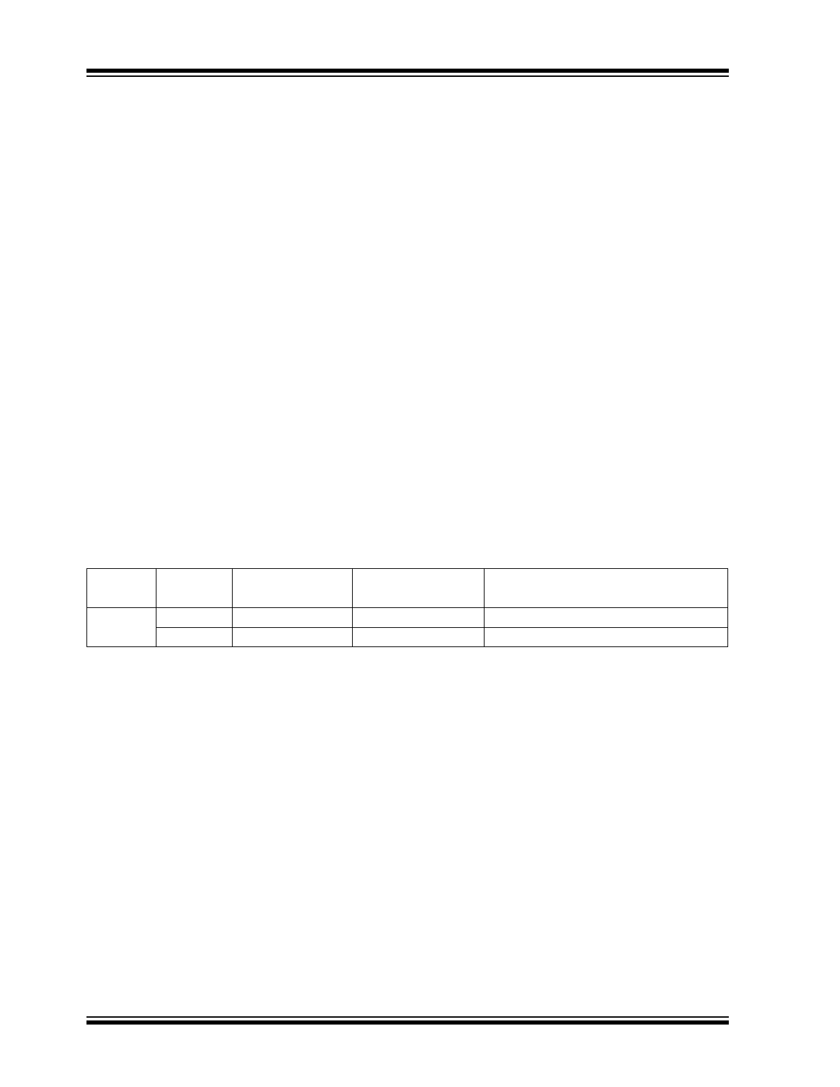
TABLE 1-1:
UPD1001 PACKAGE/PIN CONFIGURATION SUMMARY
Package
Pin Config.
Name
PD Role
USB Receptacle
Notes
32-SQFN
32-A Provider
Standard-A
(STD-A)
See
Section 2.1
for pin assignments
32-B Consumer/Provider
Standard-B
(STD-B)
See
Section 2.1
for pin assignments
2014 Microchip Technology Inc.
DS00001759B-page 5
UPD1001
FIGURE 1-1:
INTERNAL BLOCK DIAGRAM
Power
Delivery
AFE
Power
Delivery
MAC
PD_DATA
PD_ID
Configuration
Select
CFG_SEL0
CFG_SEL1
Voltage
Monitor
VMON
Clocks
Micro-
controller
SPI ROM
Controller
Current
Monitor
IMON
SPI ROM
I/O
Controller
†
I/O
†
Specific functions are determined by package and CFG_SEL0/CFG_SEL1 profile selection.
RESET_N
Reset
Controller
Voltage
Switch
†
VBUS
†
VTR
UPD1001
UPD1001
DS00001759B-page 6
2014 Microchip Technology Inc.
2.0
PIN DESCRIPTIONS AND CONFIGURATION
The pinouts for the package, along with system-level application diagrams, are detailed in the following section:
•
32-Pin SQFN (32-SQFN)
Note:
For a summary of the available pin combinations and their corresponding target applications, refer to
Table 1-1
.
Pin descriptions are detailed in
Section 2.2, "Pin Descriptions," on page 10
. For details on the CFG_SEL0 and CFG_-
SEL1 Configuration Select signals, refer to
Section 3.3, "Configuration Selection (CFG_SEL0/CFG_SEL1)," on
page 20
.
2.1
32-Pin SQFN (32-SQFN)
2.1.1
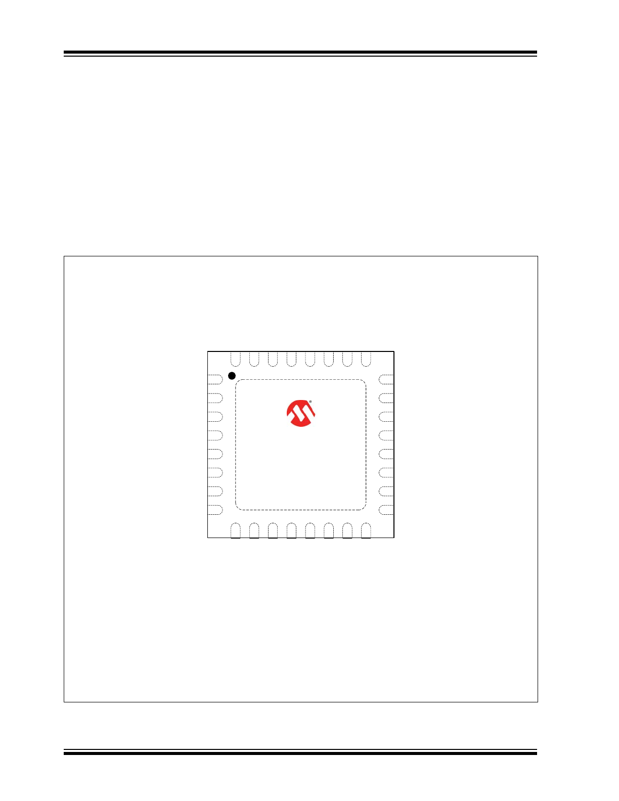
32-SQFN PIN DIAGRAM
Note:
When an “_N” is used at the end of the signal name, it indicates that the signal is active low. For example,
RESET_N indicates that the reset signal is active low.
FIGURE 2-1:
32-SQFN PIN ASSIGNMENTS (TOP VIEW)
1
2
3
4
5
6
7
8
9
10
11
12
13
14
15
16
24
23
22
21
20
19
18
17
32
31
30
29
28
27
26
25
CFG_SEL1
CFG_SEL0
IFAULT
VDD33_CAP
VBUS
VSW_CAP
VTR
VDD18A_CAP
PD_DATA
PD_ID
PD_VDD18
VDDIO
IMON
VMON
VS
E
L
3_
N
VSEL2_N
VB
U
S
_DISC
H
ARGE
FAULT
_
N
VS
E
L
1_
N
P
D
_
D
ET
EC
T/
VS
A
F
ED
B_
E
N
*
IN
SER
T
IO
N
_
DET
E
C
T
/B
ULK_CAP*
SP
I_
RO
M
_
D
I
SPI
_
ROM_DO
SPI_ROM
_
CLK
SPI_ROM
_
CE_N
TE
ST
VDD18_CAP
RE
SET
_
N
CHG_EMU
_
EN/NC*
VS
E
L
0_
N
V
DDIO
PD_EN_N
(Connect exposed pad to ground with a via field)
VSS
UPD1001
32-SQFN
( T o p V i e w )
Note: Exposed pad (VSS) on bottom of package must be connected to ground with a via field.
*The functionality of this pin is dependent on the CFG_SEL0/CFG_SEL1 profile selection.

2014 Microchip Technology Inc.
DS00001759B-page 7
UPD1001
Note:
The buffer type for each signal is indicated in the BUFFER TYPE column of
Table 2-2, "Pin Descriptions"
.
A description of the buffer types is provided in
Section 2.3, "Buffer Types"
.
2.1.2
32-SQFN PIN ASSIGNMENTS
The UPD1001 32-SQFN provides two distinct pin configurations (32-A and 32-B) based upon the CFG_SEL0 and
CFG_SEL1 Configuration Select pins. The 32-A and 32-B pin configurations are designed for use with USB Standard-
A and Standard-B receptacles, respectively, and are detailed in
Table 2-1
. For pin descriptions, refer to
Section 2.2, "Pin
Descriptions"
. For example connection diagrams, refer to
Section 2.4, "Power Connection Diagram," on page 18
. For
information on the Configuration Select pins, refer to
Section 3.3, "Configuration Selection (CFG_SEL0/CFG_SEL1)"
.
Note:
The 32-A and 32-B pin configuration assignments differ only on pins 14, 15, and 16.
TABLE 2-1:
32-SQFN PACKAGE PIN ASSIGNMENTS
Pin Number
Configuration 32-A Name
Configuration 32-B Name
1
CFG_SEL0
2
CFG_SEL1
3
IFAULT
4
VDD33_CAP
5
VBUS
6
VSW_CAP
7
VTR
8
VDD18A_CAP
9
SPI_ROM_CE_N
10
SPI_ROM_CLK
11
SPI_ROM_DO
12
SPI_ROM_DI
13
VDDIO
14
INSERTION_DETECT
BULK_CAP
15
PD_DETECT
SAFEDB_EN
16
CHG_EMU_EN
NC
17
VMON
18
IMON
19
VDDIO
20
VDD18_CAP
21
PD_VDD18
22
PD_EN_N
23
PD_ID
24
PD_DATA
25
VBUS_DISCHARGE
26
TEST
27
RESET_N
28
VSEL0_N
UPD1001
DS00001759B-page 8
2014 Microchip Technology Inc.
2.1.3
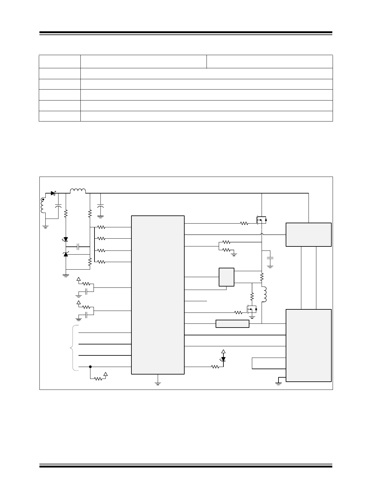
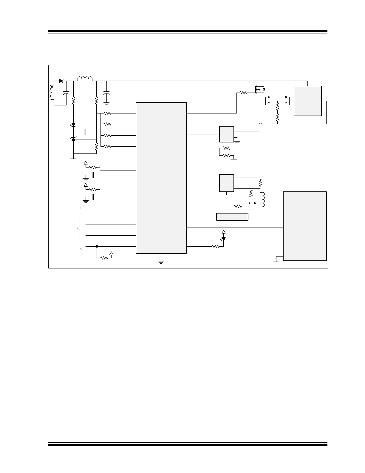
32-SQFN SYSTEM LEVEL DIAGRAMS
Figure 2-2
and
Figure 2-3
provide typical system level diagrams of the UPD1001 for 32-A (Standard-A receptacle) and
32-B (Standard-B receptacle) applications, respectively.
29
VSEL1_N
30
VSEL2_N
31
VSEL3_N
32
FAULT_N
Exposed Pad
VSS
FIGURE 2-2:
CONFIGURATION 32-A SYSTEM-LEVEL DIAGRAM
TABLE 2-1:
32-SQFN PACKAGE PIN ASSIGNMENTS (CONTINUED)
Pin Number
Configuration 32-A Name
Configuration 32-B Name
Microchip
UPD1001
32-SQFN
Configuration
32-A
SPI_ROM_CLK
SPI_ROM_DI
SPI_ROM_DO
SPI_ROM_CE_N
To
SP
I R
O
M
VSS
+
+
PD_EN_N
CHG_EMU_EN
CFG_SEL0
VDDIO
CFG_SEL1
VDDIO
USB
Power
Delivery
Enabled
Standard-A
Receptacle
Port Power
Controller
VDDIO
VMON
IMON
CSA
+
CMP
IFAULT
D+
D-
GND
PD_DETECT 1
VBUS_DISCHARGE
VBUS
Couple/Filter
PD_DATA
PD_ID
PD_DETECT
INSERTION_DETECT
INSERTION_DETECT 2
INSERTION_DETECT 1
SHIELD
35.7k
5.1k
VDDIO
FAULT_N
VSEL0_N
VSEL1_N
VSEL2_N
VSEL3_N
2014 Microchip Technology Inc.
DS00001759B-page 9
UPD1001
FIGURE 2-3:
CONFIGURATION 32-B SYSTEM-LEVEL DIAGRAM
Microchip
UPD1001
32-SQFN
Configuration
32-B
VSEL0_N
VSEL1_N
SPI_ROM_CLK
SPI_ROM_DI
SPI_ROM_DO
SPI_ROM_CE_N
To
SP
I R
O
M
VSS
+
+
PD_EN_N
VSAFEDB_EN
CFG_SEL0
VDDIO
CFG_SEL1
VDDIO
USB
Power
Delivery
Enabled
Standard-B
Receptacle
Dead
Battery
VDDIO
VMON
IMON
CSA
+
CMP
IFAULT
GND
ID
VBUS_DISCHARGE
VBUS
Couple/Filter
PD_DATA
PD_ID
BULK_CAP
Filter
Cap
Bank
35.7k
5.1k
VDDIO
FAULT_N
VSEL2_N
VSEL3_N
UPD1001
DS00001759B-page 10
2014 Microchip Technology Inc.
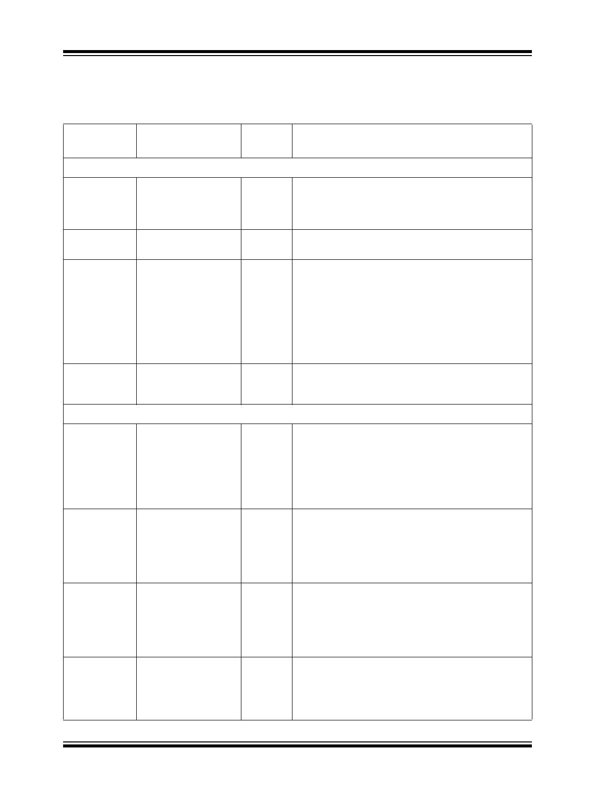
2.2
Pin Descriptions
TABLE 2-2:
PIN DESCRIPTIONS
Name
Symbol
Buffer
Type
Description
Power Delivery
Power Deliv-
ery Cable ID
PD_ID
AIO
USB connector signal used to indicate a high-current
power delivery capable cable is inserted. This signal is to
be connected to the PD_ID pin located on the USB PD
Standard-B receptacle.
Power Deliv-
ery VBUS Data
PD_DATA
AIO
Modulated power delivery VBUS data. Requires in-line
isolation filter. Reference schematic available on request.
Power Deliv-
ery Detect
PD_DETECT
IS
(PU)
This signal is to be connected to the PD DETECT pins
located on the USB PD Standard-A receptacle. This sig-
nal is pulled high via an internal pull-up resistor by
default. Assertion (low value) of PD_DETECT qualifies a
USB-PD plug detection event.
Note:
This function is only available in specific
device configurations.
Power
Delivery
Enable
PD_EN_N
O8
This active low signal controls output of the power supply
voltage onto VBUS. This signal will typically always be
asserted, even when VBUS is 5 V.
Miscellaneous
VBUS Voltage
Monitor
VMON
AI
Stepped down voltage representation of the VBUS volt-
age. This signal must be connected to a voltage divider
circuit as specified in
Section 2.4, "Power Connection
Diagram," on page 18
. Voltage must not exceed 5 V on
this signal. Refer to
Section 3.4, "Voltage/Current Moni-
tors (VMON/IMON)," on page 25
for additional informa-
tion.
Charger Cur-
rent Monitor
IMON
AI
Voltage representation of the charger current. This signal
should be fed by a current sense amplifier tuned to output
3.0 V when 6.0 A is flowing on VBUS. Voltage must not
exceed 5 V on this signal. Refer to
Section 3.4, "Voltage/
Current Monitors (VMON/IMON)," on page 25
for addi-
tional information.
Power Supply
Fault Indicator
FAULT_N
OD8
This active low signal can be connected to an external
LED or SoC and is used by the device to indicate power
supply exceptions/failures as determined by the inte-
grated voltage/current monitors. Refer to
Section 3.4,
"Voltage/Current Monitors (VMON/IMON)," on page 25
for additional information.
Power Deliv-
ery Profile
Configuration
Selector 0
CFG_SEL0
AIO
This pin is used in conjunction with CFG_SEL1 to select
the power delivery profile of the device via an externally
connected RC circuit. Refer to
Section 3.3, "Configuration
Selection (CFG_SEL0/CFG_SEL1)"
for additional infor-
mation.
2014 Microchip Technology Inc.
DS00001759B-page 1
Highlights
• Integrated USB Power Delivery (PD) PHY
• Support for Power Delivery Message Protocol
• Integrated Voltage and Current ADC Inputs
• Configuration Profile Selection
• On-chip Microcontroller
• SPI Interface
• Commercial and Industrial Grade Temperature
Support
• Available in 32-SQFN Package
Target Applications
• AC Adapters & Chargers
- Type-A
- Type-B
- Micro-A
- Micro-B
- Captive cable
Key Benefits
• Integrated USB Power Delivery (PD) PHY
- Integrated receive termination
- Requires minimal external components
• Support for Power Delivery Message Protocol
- Message Generation/Consumption
- Retry Generation
- Error Handling
- State Behavior
• Cable Detect Logic
- Cable attachment type
• CFG_SEL pins allow selection of multiple profiles
- Provider
- Consumer/Provider
• Integrated Voltage (VMON) and Current (IMON)
ADC Inputs
• Dead Battery Support
• On-chip Microcontroller
- Manages I/Os and other signals
- Implements power delivery policy engine and
device policy manager
• Configuration Programming via OTP, or Vendor
Defined Messaging
• Supports Low Power Modes
• Serial Peripheral Interface (SPI) Bus
• Internal 3.3 V and 1.8 V Voltage Regulators
• Integrated Oscillator Reduces BOM Costs
• Package
- 32-pin SQFN (5 x 5 mm)
• Environmental
- Commercial temperature range (0°C to +70°C)
- Industrial temperature range (-40°C to +85°C
UPD1001
USB Power Delivery Controller
UPD1001
DS00001759B-page 2
2014 Microchip Technology Inc.
TO OUR VALUED CUSTOMERS
It is our intention to provide our valued customers with the best documentation possible to ensure successful use of your Microchip
products. To this end, we will continue to improve our publications to better suit your needs. Our publications will be refined and
enhanced as new volumes and updates are introduced.
If you have any questions or comments regarding this publication, please contact the Marketing Communications Department via
E-mail at
docerrors@microchip.com
. We welcome your feedback.
Most Current Documentation
To obtain the most up-to-date version of this documentation, please register at our Worldwide Web site at:
http://www.microchip.com
You can determine the version of a data sheet by examining its literature number found on the bottom outside corner of any page.
The last character of the literature number is the version number, (e.g., DS30000000A is version A of document DS30000000).
Errata
An errata sheet, describing minor operational differences from the data sheet and recommended workarounds, may exist for cur-
rent devices. As device/documentation issues become known to us, we will publish an errata sheet. The errata will specify the
revision of silicon and revision of document to which it applies.
To determine if an errata sheet exists for a particular device, please check with one of the following:
• Microchip’s Worldwide Web site;
http://www.microchip.com
• Your local Microchip sales office (see last page)
When contacting a sales office, please specify which device, revision of silicon and data sheet (include -literature number) you are
using.
Customer Notification System
Register on our web site at
www.microchip.com
to receive the most current information on all of our products.
2014 Microchip Technology Inc.
DS00001759B-page 3
UPD1001
Table of Contents
1.0 Introduction ..................................................................................................................................................................................... 4
2.0 Pin Descriptions and Configuration ................................................................................................................................................. 6
3.0 Functional Descriptions ................................................................................................................................................................. 19
4.0 Operational Characteristics ........................................................................................................................................................... 33
5.0 Package Outline ............................................................................................................................................................................ 37
6.0 Revision History ............................................................................................................................................................................ 38
The Microchip Web Site ...................................................................................................................................................................... 39
Customer Change Notification Service ............................................................................................................................................... 39
Customer Support ............................................................................................................................................................................... 39
Product Identification System ............................................................................................................................................................. 40
UPD1001
DS00001759B-page 4
2014 Microchip Technology Inc.
1.0
INTRODUCTION
1.1
General Description
The UPD1001 is a USB Power Delivery (PD) controller designed to adhere to the USB Power Delivery Specification.
USB Power Delivery allows a host (or device) to provide or consume up to 5 Amps and/or up to 20 Volts of power from
a USB PD capable partner device on the other end of the USB cable. USB PD capable standard and custom cables/
connectors are supported, which in most cases are backward compatible with standard USB connections.
The UPD1001 provides a complete USB Power Delivery solution for all charger and adapter solutions. The functionality
of the UPD1001 is selected via two configuration selection pins, CFG_SEL0 and CFG_SEL1, which can be used to
select unique PD and system configurations. Designing the UPD1001 into a system can be as simple as selecting a
configuration, with no external EEPROM required. Advanced programmability options exist with an external EEPROM
installed.
The integrated USB Power Delivery MAC and PHY support provider and consumer operation via the PD communication
protocol, as specified in Revision 1.0 (Version 1.2) of the USB Power Delivery Specification. Monitoring of VBUS and
battery charging is accomplished via the integrated voltage and current ADC inputs. The PHY supports cable ID detec-
tion/identification and loopback modes. The PHY includes a 24MHz FSK modulator/demodulator and provides inte-
grated terminations. The USB PD MAC supports both USB PD insertion detection (cold socket) and dead battery cases.
The on-chip microcontroller manages the IOs and implements the power delivery local policy engine and device man-
ager. The SPI ROM controller is used by the microcontroller for optional external code execution from ROM. A One Time
Programmable (OTP) ROM is integrated in the UPD1001. Integrated 3.3 V and 1.8 V regulators allow device operation
from a single power supply. The UPD1001 is available in commercial (0°C to +70°C) and industrial (-40°C to +85°C)
temperature ranges. An internal block diagram of the UPD1001 is shown in
Figure 1-1
.
The UPD1001 is offered in a 32-pin SQFN package. The package provides multiple pin configurations, based upon the
CFG_SEL0 and CFG_SEL1 Configuration Select signals.
Table 1-1
summarizes the available pin combinations and
their target applications. Refer to
Section 2.0, "Pin Descriptions and Configuration," on page 6
for detailed information
on specific pin configurations.
TABLE 1-1:
UPD1001 PACKAGE/PIN CONFIGURATION SUMMARY
Package
Pin Config.
Name
PD Role
USB Receptacle
Notes
32-SQFN
32-A Provider
Standard-A
(STD-A)
See
Section 2.1
for pin assignments
32-B Consumer/Provider
Standard-B
(STD-B)
See
Section 2.1
for pin assignments
2014 Microchip Technology Inc.
DS00001759B-page 5
UPD1001
FIGURE 1-1:
INTERNAL BLOCK DIAGRAM
Power
Delivery
AFE
Power
Delivery
MAC
PD_DATA
PD_ID
Configuration
Select
CFG_SEL0
CFG_SEL1
Voltage
Monitor
VMON
Clocks
Micro-
controller
SPI ROM
Controller
Current
Monitor
IMON
SPI ROM
I/O
Controller
†
I/O
†
Specific functions are determined by package and CFG_SEL0/CFG_SEL1 profile selection.
RESET_N
Reset
Controller
Voltage
Switch
†
VBUS
†
VTR
UPD1001
UPD1001
DS00001759B-page 6
2014 Microchip Technology Inc.
2.0
PIN DESCRIPTIONS AND CONFIGURATION
The pinouts for the package, along with system-level application diagrams, are detailed in the following section:
•
32-Pin SQFN (32-SQFN)
Note:
For a summary of the available pin combinations and their corresponding target applications, refer to
Table 1-1
.
Pin descriptions are detailed in
Section 2.2, "Pin Descriptions," on page 10
. For details on the CFG_SEL0 and CFG_-
SEL1 Configuration Select signals, refer to
Section 3.3, "Configuration Selection (CFG_SEL0/CFG_SEL1)," on
page 20
.
2.1
32-Pin SQFN (32-SQFN)
2.1.1
32-SQFN PIN DIAGRAM
Note:
When an “_N” is used at the end of the signal name, it indicates that the signal is active low. For example,
RESET_N indicates that the reset signal is active low.
FIGURE 2-1:
32-SQFN PIN ASSIGNMENTS (TOP VIEW)
1
2
3
4
5
6
7
8
9
10
11
12
13
14
15
16
24
23
22
21
20
19
18
17
32
31
30
29
28
27
26
25
CFG_SEL1
CFG_SEL0
IFAULT
VDD33_CAP
VBUS
VSW_CAP
VTR
VDD18A_CAP
PD_DATA
PD_ID
PD_VDD18
VDDIO
IMON
VMON
VS
E
L
3_
N
VSEL2_N
VB
U
S
_DISC
H
ARGE
FAULT
_
N
VS
E
L
1_
N
P
D
_
D
ET
EC
T/
VS
A
F
ED
B_
E
N
*
IN
SER
T
IO
N
_
DET
E
C
T
/B
ULK_CAP*
SP
I_
RO
M
_
D
I
SPI
_
ROM_DO
SPI_ROM
_
CLK
SPI_ROM
_
CE_N
TE
ST
VDD18_CAP
RE
SET
_
N
CHG_EMU
_
EN/NC*
VS
E
L
0_
N
V
DDIO
PD_EN_N
(Connect exposed pad to ground with a via field)
VSS
UPD1001
32-SQFN
( T o p V i e w )
Note: Exposed pad (VSS) on bottom of package must be connected to ground with a via field.
*The functionality of this pin is dependent on the CFG_SEL0/CFG_SEL1 profile selection.
2014 Microchip Technology Inc.
DS00001759B-page 7
UPD1001
Note:
The buffer type for each signal is indicated in the BUFFER TYPE column of
Table 2-2, "Pin Descriptions"
.
A description of the buffer types is provided in
Section 2.3, "Buffer Types"
.
2.1.2
32-SQFN PIN ASSIGNMENTS
The UPD1001 32-SQFN provides two distinct pin configurations (32-A and 32-B) based upon the CFG_SEL0 and
CFG_SEL1 Configuration Select pins. The 32-A and 32-B pin configurations are designed for use with USB Standard-
A and Standard-B receptacles, respectively, and are detailed in
Table 2-1
. For pin descriptions, refer to
Section 2.2, "Pin
Descriptions"
. For example connection diagrams, refer to
Section 2.4, "Power Connection Diagram," on page 18
. For
information on the Configuration Select pins, refer to
Section 3.3, "Configuration Selection (CFG_SEL0/CFG_SEL1)"
.
Note:
The 32-A and 32-B pin configuration assignments differ only on pins 14, 15, and 16.
TABLE 2-1:
32-SQFN PACKAGE PIN ASSIGNMENTS
Pin Number
Configuration 32-A Name
Configuration 32-B Name
1
CFG_SEL0
2
CFG_SEL1
3
IFAULT
4
VDD33_CAP
5
VBUS
6
VSW_CAP
7
VTR
8
VDD18A_CAP
9
SPI_ROM_CE_N
10
SPI_ROM_CLK
11
SPI_ROM_DO
12
SPI_ROM_DI
13
VDDIO
14
INSERTION_DETECT
BULK_CAP
15
PD_DETECT
SAFEDB_EN
16
CHG_EMU_EN
NC
17
VMON
18
IMON
19
VDDIO
20
VDD18_CAP
21
PD_VDD18
22
PD_EN_N
23
PD_ID
24
PD_DATA
25
VBUS_DISCHARGE
26
TEST
27
RESET_N
28
VSEL0_N
UPD1001
DS00001759B-page 8
2014 Microchip Technology Inc.
2.1.3
32-SQFN SYSTEM LEVEL DIAGRAMS
Figure 2-2
and
Figure 2-3
provide typical system level diagrams of the UPD1001 for 32-A (Standard-A receptacle) and
32-B (Standard-B receptacle) applications, respectively.
29
VSEL1_N
30
VSEL2_N
31
VSEL3_N
32
FAULT_N
Exposed Pad
VSS
FIGURE 2-2:
CONFIGURATION 32-A SYSTEM-LEVEL DIAGRAM
TABLE 2-1:
32-SQFN PACKAGE PIN ASSIGNMENTS (CONTINUED)
Pin Number
Configuration 32-A Name
Configuration 32-B Name
Microchip
UPD1001
32-SQFN
Configuration
32-A
SPI_ROM_CLK
SPI_ROM_DI
SPI_ROM_DO
SPI_ROM_CE_N
To
SP
I R
O
M
VSS
+
+
PD_EN_N
CHG_EMU_EN
CFG_SEL0
VDDIO
CFG_SEL1
VDDIO
USB
Power
Delivery
Enabled
Standard-A
Receptacle
Port Power
Controller
VDDIO
VMON
IMON
CSA
+
CMP
IFAULT
D+
D-
GND
PD_DETECT 1
VBUS_DISCHARGE
VBUS
Couple/Filter
PD_DATA
PD_ID
PD_DETECT
INSERTION_DETECT
INSERTION_DETECT 2
INSERTION_DETECT 1
SHIELD
35.7k
5.1k
VDDIO
FAULT_N
VSEL0_N
VSEL1_N
VSEL2_N
VSEL3_N
2014 Microchip Technology Inc.
DS00001759B-page 9
UPD1001
FIGURE 2-3:
CONFIGURATION 32-B SYSTEM-LEVEL DIAGRAM
Microchip
UPD1001
32-SQFN
Configuration
32-B
VSEL0_N
VSEL1_N
SPI_ROM_CLK
SPI_ROM_DI
SPI_ROM_DO
SPI_ROM_CE_N
To
SP
I R
O
M
VSS
+
+
PD_EN_N
VSAFEDB_EN
CFG_SEL0
VDDIO
CFG_SEL1
VDDIO
USB
Power
Delivery
Enabled
Standard-B
Receptacle
Dead
Battery
VDDIO
VMON
IMON
CSA
+
CMP
IFAULT
GND
ID
VBUS_DISCHARGE
VBUS
Couple/Filter
PD_DATA
PD_ID
BULK_CAP
Filter
Cap
Bank
35.7k
5.1k
VDDIO
FAULT_N
VSEL2_N
VSEL3_N
UPD1001
DS00001759B-page 10
2014 Microchip Technology Inc.
2.2
Pin Descriptions
TABLE 2-2:
PIN DESCRIPTIONS
Name
Symbol
Buffer
Type
Description
Power Delivery
Power Deliv-
ery Cable ID
PD_ID
AIO
USB connector signal used to indicate a high-current
power delivery capable cable is inserted. This signal is to
be connected to the PD_ID pin located on the USB PD
Standard-B receptacle.
Power Deliv-
ery VBUS Data
PD_DATA
AIO
Modulated power delivery VBUS data. Requires in-line
isolation filter. Reference schematic available on request.
Power Deliv-
ery Detect
PD_DETECT
IS
(PU)
This signal is to be connected to the PD DETECT pins
located on the USB PD Standard-A receptacle. This sig-
nal is pulled high via an internal pull-up resistor by
default. Assertion (low value) of PD_DETECT qualifies a
USB-PD plug detection event.
Note:
This function is only available in specific
device configurations.
Power
Delivery
Enable
PD_EN_N
O8
This active low signal controls output of the power supply
voltage onto VBUS. This signal will typically always be
asserted, even when VBUS is 5 V.
Miscellaneous
VBUS Voltage
Monitor
VMON
AI
Stepped down voltage representation of the VBUS volt-
age. This signal must be connected to a voltage divider
circuit as specified in
Section 2.4, "Power Connection
Diagram," on page 18
. Voltage must not exceed 5 V on
this signal. Refer to
Section 3.4, "Voltage/Current Moni-
tors (VMON/IMON)," on page 25
for additional informa-
tion.
Charger Cur-
rent Monitor
IMON
AI
Voltage representation of the charger current. This signal
should be fed by a current sense amplifier tuned to output
3.0 V when 6.0 A is flowing on VBUS. Voltage must not
exceed 5 V on this signal. Refer to
Section 3.4, "Voltage/
Current Monitors (VMON/IMON)," on page 25
for addi-
tional information.
Power Supply
Fault Indicator
FAULT_N
OD8
This active low signal can be connected to an external
LED or SoC and is used by the device to indicate power
supply exceptions/failures as determined by the inte-
grated voltage/current monitors. Refer to
Section 3.4,
"Voltage/Current Monitors (VMON/IMON)," on page 25
for additional information.
Power Deliv-
ery Profile
Configuration
Selector 0
CFG_SEL0
AIO
This pin is used in conjunction with CFG_SEL1 to select
the power delivery profile of the device via an externally
connected RC circuit. Refer to
Section 3.3, "Configuration
Selection (CFG_SEL0/CFG_SEL1)"
for additional infor-
mation.