

2014-2017 Microchip Technology Inc.
DS20005285D-page 1
RE46C200
Features
• 6.5-12V Operation
• Low Quiescent Current
• Programmable Internal Infrared Emitter Diode
(IRED) Current
• Programmable Standby Alarm Level
• Programmable Hush
™
Alarm Level
• Programmable Hysteresis Alarm Level
• Programmable Chamber Test Alarm Level
• Programmable Low Battery Test
• Programmable Low-Battery Hush
• Programmable Horn Pattern
• Horn Synchronization
• 10-year End-of-Life Indication
• Differentiated Chamber Fail and Low Battery
Warnings
• Local Alarm Memory
• Interconnect up to 40 Detectors
• IO Filter and Charge Dump
• Smart IO for CO alarm Option
• 9-Minute or 80-Second Hush Timer
• Smart Hush
®
Option
• Automatic Alarm Locate for Interconnected Units
Description
The RE46C200 is a next generation low power CMOS
photoelectric-type smoke detector IC. With minimal
external components, this circuit will provide all the
required features for a photoelectric-type smoke
detector.
The design incorporates a gain selectable photo
amplifier for use with an infrared emitter/detector pair.
An on-chip oscillator strobes power to the smoke
detection circuitry for 5 ms every 10 seconds to keep
standby current to a minimum.
A check for a low battery condition is performed every
80 seconds and chamber test is performed once every
320 seconds when in standby. The temporal horn
pattern supports the NFPA 72 emergency evacuation
signal.
An interconnect pin allows multiple detectors to be
connected such that when one unit alarms, all units will
sound. A charge dump feature will quickly discharge
the interconnect line when exiting a local alarm. The
interconnect input is also digitally filtered.
An internal 9-minute or 80-second timer is used for a
Hush operation.
A local alarm memory feature allows the user to
determine if the unit has previously entered a local
alarm condition.
Utilizing low power CMOS technology, the RE46C200
is designed for use in smoke detectors that comply with
Underwriters Laboratory Specification UL217 and
UL268.
Pin Configuration
RE46C200
PDIP, SOIC
IRP
1
2
3
4
5
6
7
14
13
12
11
10
9
8
IRN
V
DD
TESTOUT
IRED
V
SS
HB
TEST
TEST2
IO
GLED
RLED
FEED
HS
9V Programmable Photoelectric Smoke Detector ASIC
RE46C200
DS20005285D-page 2
2014-2017 Microchip Technology Inc.
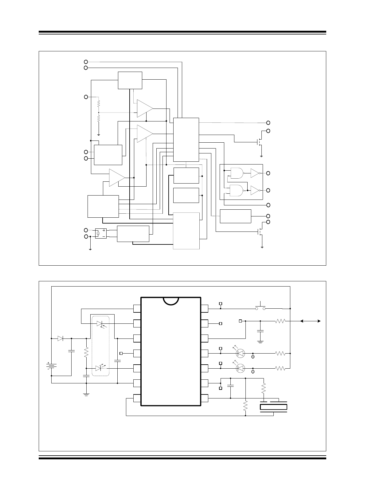
Functional Block Diagram
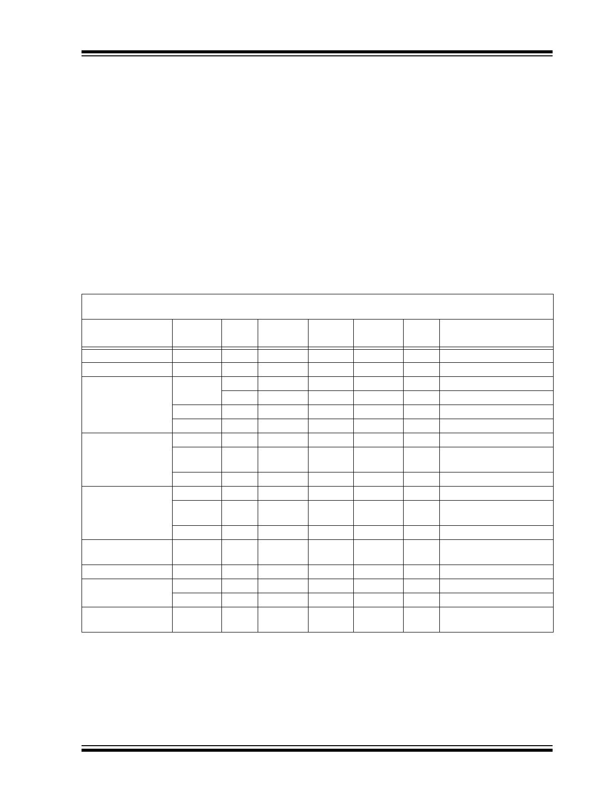
Typical Application
&RQWURO/RJLF
DQG7LPLQJ
7ULPPHG
2VFLOODWRU
325DQG%,$6
9
''
,51
,5('
7(67
5
5
)(('
+6
5/('
*/('
+%
,53
9
66
,QWHUFRQQHFW
3URJUDPPDEOH
,5('&XUUHQW
3URJUDPPDEOH
*DLQ5HIHUHQFH
3KRWR,QWHJUDWRU
3UHFLVLRQ
5HIHUHQFH
7(67
+RUQ'ULYHU
,2
/RZ%DWWHU\
&RPSDUDWRU
6PRNH
&RPSDUDWRU
3URJUDPPLQJ
&RQWURO
+LJK
1RUPDO
+\VWHUHVLV
7(67287
Push To Test
9V
Battery
R1
390ȍ
D4
C5
1.0 nF
R6
1.5 Mȍ
R5
220 kȍ
C3
100 μF
D2
D3
1
2
3
4
5
6
7
14
13
12
11
10
9
8
V
DD
IRP
IRN
TESTOUT
V
SS
I/O
IRED
HORNB
HORNS
FEED
RLED
GLED
TEST2
TEST
C4
1 μF
To Other
Units
C2
10 μF
R3
1 kȍ
Test
pads to
V
SS
Test pad
Test
pads
D5
R2
390ȍ
R4
100ȍ
D1
C1
100 nF
Note 1: R5, R6 and C5 are typical values and may be adjusted to maximize sound pressure.
2: C1 should be located as close as possible to the device power pins.
3: No internal reverse battery protection. External reverse battery protection (for example: D1) circuitry required.
2014-2017 Microchip Technology Inc.
DS20005285D-page 3
RE46C200
1.0
ELECTRICAL
CHARACTERISTICS
Absolute Maximum Ratings
†
V
DD
.................................................................................12.5V
Voltage Range Except FEED, IO, IRP, IRN ........................... .
.............................................................V
IN
= - .3 to V
DD
+ .3V
FEED Input Voltage Range.................... V
INFD
= -10 to + 22V
IO Input Voltage Range............................... V
IO1
= - .3 to 15V
IRP/IRN Input Voltage Range ................. V
INIRD
= - .3 to 5.5V
Input Current Except FEED .................................. I
IN
= 10 mA
Operating Temperature .............................. T
A
= -10 to +60
Ԩ
Storage Temperature ............................ T
STG
= -55 to +125
Ԩ
Maximum Junction Temperature .......................... T
J
= +150
Ԩ
MM ESD..........................................................................150V
†Notice: Stresses above those listed under “Maximum
ratings” may cause permanent damage to the device.
This is a stress rating only and functional operation of
the device at these or any other conditions above those
indicated in the operation listings of this specification is
not implied. Exposure to maximum rating conditions for
extended periods may affect device reliability.
.
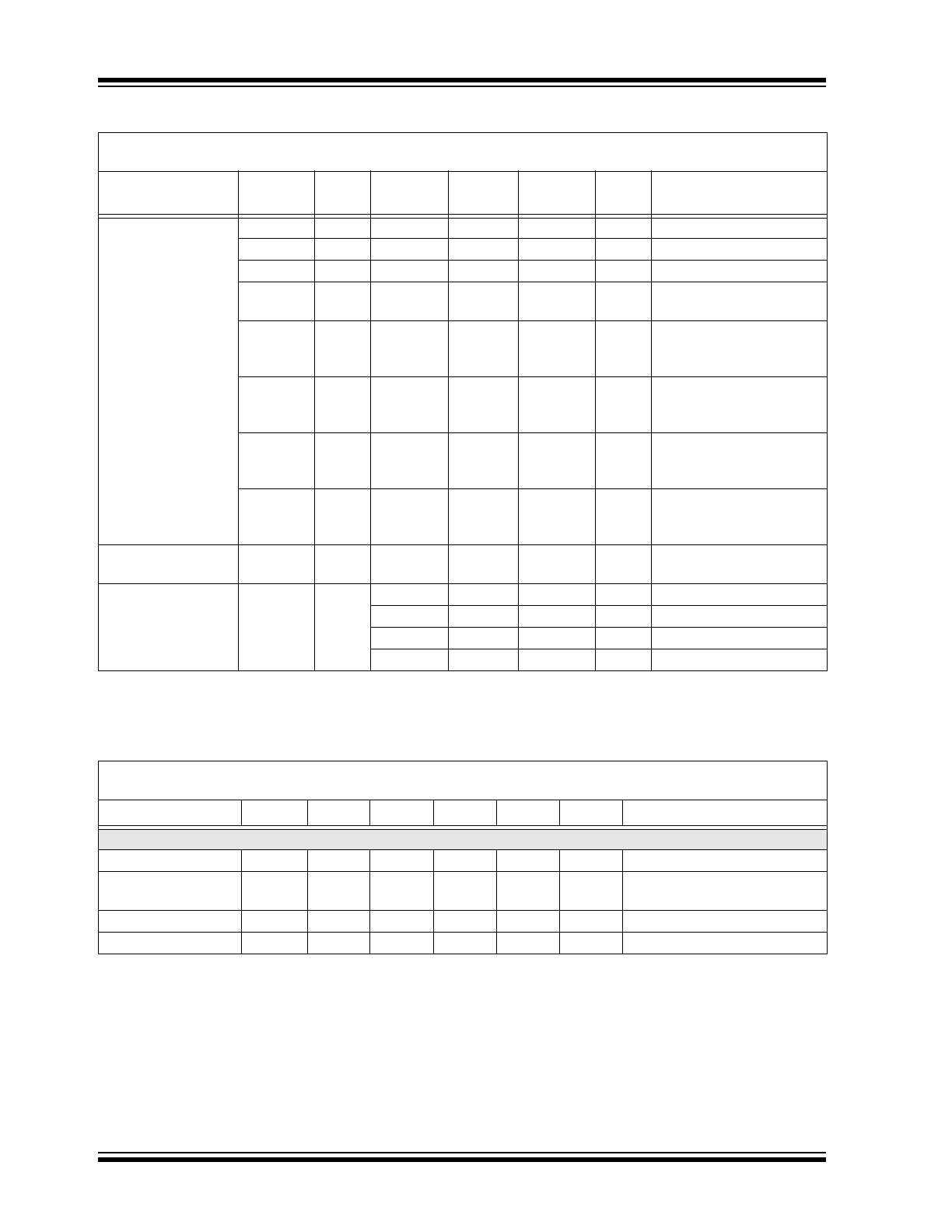
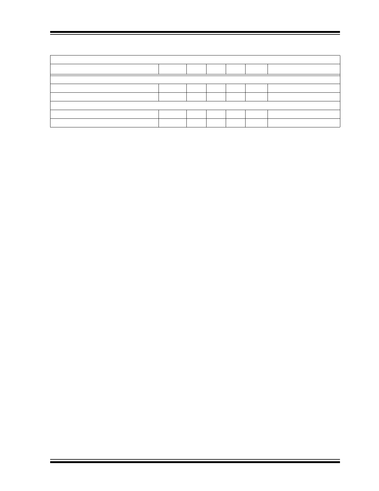
DC ELECTRICAL CHARACTERISTICS
DC Electrical Characteristics: Unless otherwise indicated, all parameters apply at T
A
= -10 to +60°C, V
DD
= 9V,
V
SS
= 0V (
Note 1
)
Parameter
Symbol
Test
Pin
Min.
Typ.
Max.
Units
Conditions
Supply Voltage
V
DD
3
6.5
—
12
V
Operating
Supply Current
I
DD
3
—
0.9
1.5
µA
Standby
Input Leakage
L
INOP
1
-200
—
200
pA
IRP = 5V or V
SS
2
-200
—
200
pA
IRN = 5V
or V
SS
I
HFD1
9
—
20
50
µA
FEED = 22V
I
ILFD1
9
-50
-15
—
µA
FEED = -10V
Input Voltage Low
V
IL1
9
—
—
2.7
V
FEED
V
IL2
12
—
—
1
V
No local alarm,
IO as an input
V
IL3
13, 14
—
—
3.4
V
TEST or TEST2
Input Voltage High
V
IH1
9
6.2
—
—
V
FEED; V
BST
= 9V
V
IH2
12
3.0
—
—
V
No local alarm,
IO as an input
V
IL3
13, 14
5.6
—
—
V
TEST or TEST2
Input Pull Down
Current
I
PD1
13,14
20
50
80
µA
V
IN
= V
DD
Output Voltage High
V
OH1
7,8
5.5
—
—
V
I
OH
= -16 mA, V
DD
= 6.5V
Output Voltage Low
V
OL1
7,8
—
—
1
V
I
OL
= 16 mA, V
DD
= 6.5V
V
OL2
10,11
—
—
0.6
V
I
OL
= 10 mA, V
DD
= 6.5V
Output Off Leakage
High
I
IOHZ
10,11
—
—
1
µA
Outputs Off, V
IN
= V
DD
Note 1: Production tested at room temperature with temperature guard-banded limits.
2: Not production tested.
RE46C200
DS20005285D-page 4
2014-2017 Microchip Technology Inc.
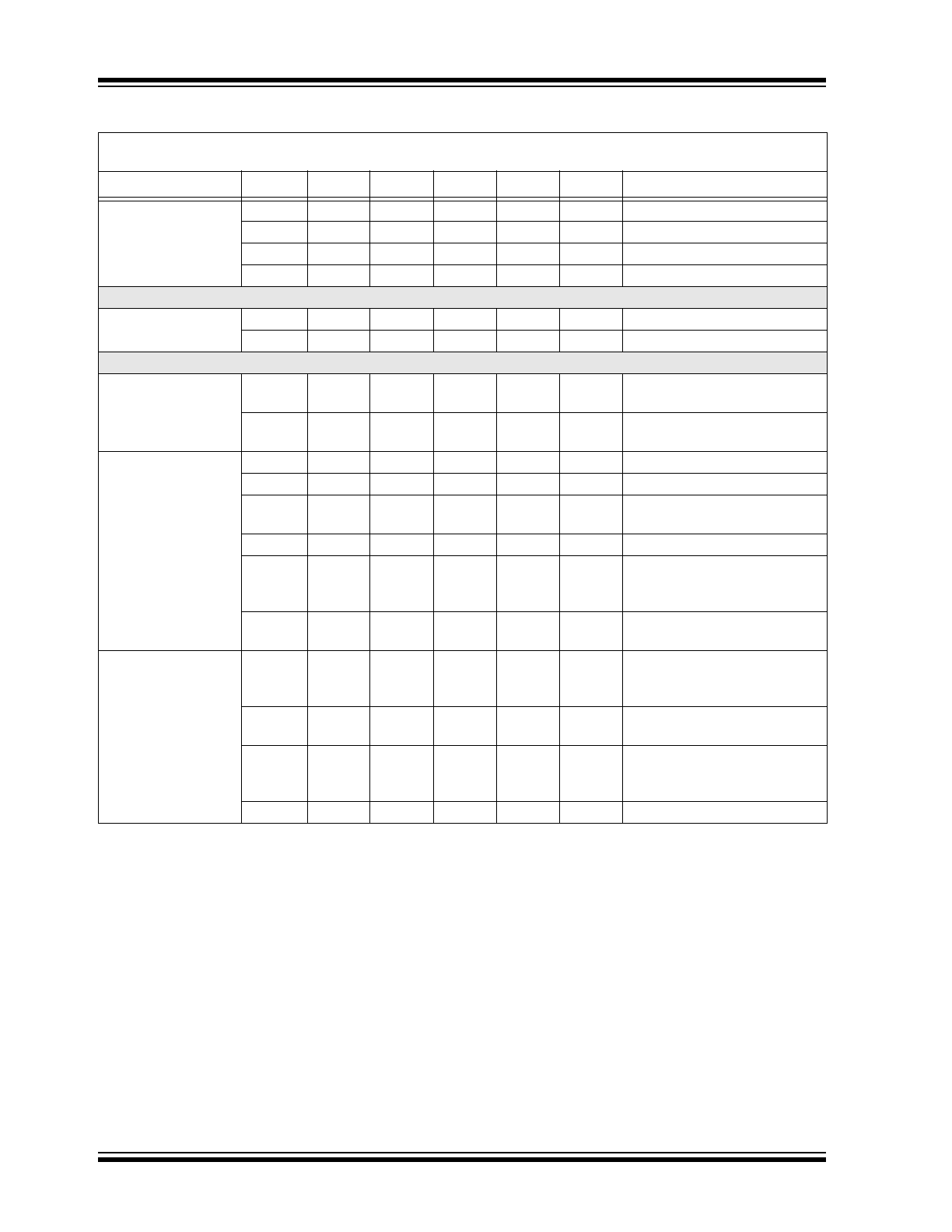
Output Current
I
IOL1
12
20
50
80
µA
V
IN
= V
DD
I
IOL2
12
—
150
µA
V
IN
= 15v
I
IOH1
12
-4
—
-16
mA
Alarm, V
IO
= 4V or V
IO
= 0V
I
IODMP
12
5
—
—
mA
At Conclusion of Local
Alarm or Test, V
IO
= 1V
I
IRED50
5
45
50
55
mA
IRED on; V
IRED
= 1.5V;
(50 mA option selected;
T
A
= +27°C)
I
IRED100
5
90
100
110
mA
IRED on; V
IRED
= 1.5V;
(100 mA option selected;
T
A
= +27°C)
I
IRED150
5
135
150
165
mA
IRED on; V
IRED
= 1.5V;
(150 mA option selected;
T
A
= +27°C
I
IRED200
5
180
200
220
mA
IRED on; V
IRED
= 1.5V;
(200 mA option selected;
T
A
= +27°C)
IRED Temperature
Coefficient
T
CIRED
5
—
0.5
—
%/ºC
IRED Output Current
(
Note 2
)
Low Battery Alarm
Voltage
V
LB
3
6.75
6.9
7.05
V
6.9V setting
7.05
7.2
7.35
V
7.2V setting
7.35
7.5
7.65
V
7.5V setting
7.65
7.8
7.95
V
7.8V setting
AC ELECTRICAL CHARACTERISTICS
AC Electrical Characteristics: Unless otherwise indicated, all parameters apply at T
A
= -10° to +60°C, V
DD
= 9V,
V
ss
= 0V.
Parameter
Symbol Test Pin
Min.
Typ.
Max.
Units
Condition
Time Base
Oscillator Period
T
POSC
593
625
657
µs
Operating,
Note 2
Oscillator Pulse
Width
T
PW
296
312
329
µs
Operating
Oscillator Tolerance
T
TOL
-5%
0
5%
%
Operating
Clock Period
T
PCLK
9.5
10
10.5
ms
Operating
Note 1: Typical values are for design information and not verified.
2: TPOSC is 100% production tested. All other timing is verified by functional testing.
3: See timing diagram for CO alarm horn pattern.
4: See timing diagram for temporal and continuous horn pattern.
5: See timing diagram for horn synchronization and AAL.
DC ELECTRICAL CHARACTERISTICS (CONTINUED)
DC Electrical Characteristics: Unless otherwise indicated, all parameters apply at T
A
= -10 to +60°C, V
DD
= 9V,
V
SS
= 0V (
Note 1
)
Parameter
Symbol
Test
Pin
Min.
Typ.
Max.
Units
Conditions
Note 1: Production tested at room temperature with temperature guard-banded limits.
2: Not production tested.

2014-2017 Microchip Technology Inc.
DS20005285D-page 5
RE46C200
RLED Indicator
LED On Time
T
ON1
10
9.5
10
10.5
ms
Operating
LED Off Time
T
LOF1
10
304
320
336
s
Standby, No Alarm
T
LOF2
10
0.94
0.99
1.04
s
Local Alarm Condition
T
LOF3
10
9.5
10
10.5
s
Timer mode, No Local Alarm
LED Period
T
PLED0
10
LED IS NOT ON
Remote Alarm only
T
PLED1
10
304
320
336
s
Standby, No Alarm
T
PLED2
10
0.95
1
1.05
s
Local Alarm Condition
T
PLED3
10
9.5
10
10.5
s
Hush mode,
No Local Alarm
GLED Indicator
LED On Time
T
ON1
11
9.5
10
10.5
ms
Operating
LED Off Time
T
OFLED1
11
0.94
0.99
1.04
s
Alarm Memory LED Pulse Train
(3x) Off Time
T
OFLED2
11
36.1
38
39.9
s
Alarm Memory LED Off Time
Between Pulse Train (3x)
T
LOF4
11
228
240
252
ms
Alarm Memory Indication
in PTT
LED Period
T
PLED4
11
238
250
263
ms
Alarm Memory Indication
in PTT
T
PLED5
11
38
40
42
s
Alarm Memory LED Timer Set
Alarm Memory
Indication Timeout
Period
T
AMTO
11
22.8
24
25.2
Hours
Alarm memory set,
AMTO<2:1> = 00
45.6
48
50.4
Hours
Alarm memory set,
AMTO<2:1> = 01
0
0
0
—
AMTO<2:1> = 10;
No alarm memory indication
∞
∞
∞
—
Alarm memory set,
AMTO<2:1> = 11;
Smoke Check
Smoke Test Period
IRED
T
STPER0
4, 5
9.5
10
10.5
s
Standby, No Alarm
T
STPER1
4, 5
0.95
1
1.05
s
Standby, one or more Valid
Smoke Samples
T
STPER2
4, 5
237
250
263
ms
Push button Test, not in alarm
T
STPER3
4, 5
0.95
1
1.05
s
Local Alarm (three consecutive
Valid Smoke Samples)
T
STPER4
4, 5
9.5
10
10.5
s
In Remote Alarm
Chamber Test Period
T
PCT1
4, 5
304
320
336
s
Chamber Test, No Alarm
AC ELECTRICAL CHARACTERISTICS (CONTINUED)
AC Electrical Characteristics: Unless otherwise indicated, all parameters apply at T
A
= -10° to +60°C, V
DD
= 9V,
V
ss
= 0V.
Parameter
Symbol Test Pin
Min.
Typ.
Max.
Units
Condition
Note 1: Typical values are for design information and not verified.
2: TPOSC is 100% production tested. All other timing is verified by functional testing.
3: See timing diagram for CO alarm horn pattern.
4: See timing diagram for temporal and continuous horn pattern.
5: See timing diagram for horn synchronization and AAL.
RE46C200
DS20005285D-page 6
2014-2017 Microchip Technology Inc.
IRED On Time
T
IRON1
5
—
110
—
µs
Operating/DIAG,
Note 1
T
IRON2
5
—
220
—
µs
Operating/DIAG,
Note 1
T
IRON3
5
—
330
—
µs
Operating/DIAG,
Note 1
T
IRON4
5
—
440
—
µs
Operating/DIAG,
Note 1
Low Battery
Low Battery Check
Period
T
PLB1
76
80
84
s
Standby, no alarm, RLED off
T
PLB2
304
320
336
s
Standby, no alarm, RLED on
Horn Operation
Horn Startup Delay
T
HDLY1
7,8
475
500
525
ms
From local alarm to horn active,
temporal horn pattern
T
HDLY2
7,8
380
400
420
ms
From local alarm to horn active,
continuous horn pattern
Horn Period
T
HPER1
7,8
38
40
42
s
Low Battery, No Alarm
T
HPER2
7,8
38
40
42
s
Chamber Fail, No Alarm
T
HPER3
7,8
237
250
263
ms
Alarm Memory Active,
Push-to-Test
T
HPER4
7,8
5.5
5.8
6.1
s
CO alarm horn period,
Note 3
T
HPER5
7,8
0.47
0.5
0.53
s
Operating, Alarm Condition,
Note 4
;
Continuous horn pattern
T
HPER6
7,8
3.8
4
4.2
s
Operating, Alarm Condition,
Note 4
; Temporal horn pattern
Horn On Time
T
HON1
7,8
9.5
10
10.5
ms
Low Battery or Fail Chamber
test, No Alarm, or optional PTT
in Alarm Memory
T
HON2
7,8
475
500
525
ms
Operating, Alarm Condition,
Note 4
; Temporal horn pattern
T
HON3
7,8
332
350
368
ms
Operating, Alarm Condition,
Note 4
;
Continuous horn pattern
T
HON4
7,8
95
100
105
ms
CO alarm,
Note 3
AC ELECTRICAL CHARACTERISTICS (CONTINUED)
AC Electrical Characteristics: Unless otherwise indicated, all parameters apply at T
A
= -10° to +60°C, V
DD
= 9V,
V
ss
= 0V.
Parameter
Symbol Test Pin
Min.
Typ.
Max.
Units
Condition
Note 1: Typical values are for design information and not verified.
2: TPOSC is 100% production tested. All other timing is verified by functional testing.
3: See timing diagram for CO alarm horn pattern.
4: See timing diagram for temporal and continuous horn pattern.
5: See timing diagram for horn synchronization and AAL.

2014-2017 Microchip Technology Inc.
DS20005285D-page 7
RE46C200
Horn Off Time
T
HOF1
7,8
475
500
525
ms
Operating, Alarm Condition,
Note 4
; Temporal horn pattern
T
HOF2
7,8
1.43
1.5
1.58
s
Operating, Alarm Condition,
Note 4
; Temporal horn pattern
T
HOF3
7,8
143
150
158
ms
Operating, Alarm Condition,
Note 4
;
Continuous horn pattern
T
HOF4
7,8
37
39
41
s
Chamber Fail Horn Off Time
T
HOF5
7,8
466
490
515
ms
Chamber Fail Horn Pulse Train
Off Time
T
HOF6
7,8
95
100
105
ms
CO alarm horn off time
between pulses,
Note 3
T
HOF7
7,8
4.8
5.1
5.4
s
CO alarm horn off time
between pulse trains,
Note 3
T
HOF8
7,8
38
40
42
s
Low Battery, No Alarm
T
HOF9
7,8
228
240
252
ms
Alarm Memory
Indication in PTT
Hush Timer Operation
Hush Timer Period
T
TPER
8.5
9
9.5
Min
9 minute option
No Alarm Condition
76
80
84
s
>1 minute option
No Alarm Condition
EOL (End-of-Life)
End-of-Life Sample
Period
T
EOLPER
346
364
382
Hours
Standby, no alarms
End-of-Life (timeout)
T
EOLTO
9.5
10
10.5
Years
Standby, no alarms,
time to EOL warning
Interconnect
IO Active Delay
T
IODLY1
12
3.5
3.7
3.9
s
Local Alarm Start to IO Active
Remote Alarm Delay
T
IODLY2
12
0.77
0.81
0.86
s
Temporal Horn Pattern, No
Local Alarm, IO Active to Alarm
T
IODLY3
12
0.29
0.31
0.34
s
Continuous Horn Pattern, No
Local Alarm, IO Active to Alarm
IO Filter
T
IOFILT
12
290
ms
IO pulse width filtered
IO Pulse On Time for
CO Alarm
T
IOPW1
12
23
—
290
ms
No local alarm, two valid pulses
required for CO
IO Pulse Off Time for
CO Alarm
T
IOTO1
12
—
—
5.4
s
IO = Low
IO Charge Dump
Duration
T
IODMP
12
475
500
525
ms
At Conclusion of Local Alarm or
Test
AC ELECTRICAL CHARACTERISTICS (CONTINUED)
AC Electrical Characteristics: Unless otherwise indicated, all parameters apply at T
A
= -10° to +60°C, V
DD
= 9V,
V
ss
= 0V.
Parameter
Symbol Test Pin
Min.
Typ.
Max.
Units
Condition
Note 1: Typical values are for design information and not verified.
2: TPOSC is 100% production tested. All other timing is verified by functional testing.
3: See timing diagram for CO alarm horn pattern.
4: See timing diagram for temporal and continuous horn pattern.
5: See timing diagram for horn synchronization and AAL.

RE46C200
DS20005285D-page 8
2014-2017 Microchip Technology Inc.
Horn Synchronization
IO Pulse Period
T
PIO1
12
3.8
4
4.2
s
Local alarm, temporal horn
pattern, SyncEn = 1,
Note 5
IO Pulse On Time
T
ONIO
12
3.41
3.59
3.77
s
Local alarm, temporal horn
pattern, SyncEn = 1,
Note 5
Horn Sync IO Dump
T
IODMP2
12
95
100
105
ms
Local alarm, SyncEn = 1,
IO dump active,
Note 4
Horn Sync IO Dump
Delay
T
IODLY4
12
285
300
315
ms
Local alarm, SyncEn = 1,
Note 5
Horn Sync Conten-
tion Window
T
IOCW
12
294
310
326
ms
Local alarm, SyncEn = 1,
IO = 0, no IO dump,
IO pull-down,
Note 5
Auto Alarm Locate (AAL)
IO Cycle Period
T
PIO2
12
15.2
16
16.8
s
Local alarm, temporal horn
pattern, SyncEn = 1,
NoAAL = 0,
Note 5
IO Cycle Off Time
T
OFIO
12
4.19
4.41
4.63
s
Local alarm, temporal horn
pattern, SyncEn = 1,
NoAAL = 0, IO off time
between IO pulse trains (3x),
Note 5
Test Mode
Input Pulse Width in
Test modes
T
TMPW
9,12,
10
µs
Input Pulse width, high or low
13,14
Inputs FEED, IO, TEST2, TEST
Data Setup Time In
Serial Read/Write
modes
T
TMSU
9,14
10
µs
Data(TEST) setup time before
CLK(FEED) in TM1/3/19
Data Hold Time In
Serial Read/Write
modes
T
TMH
9,14
10
µs
Data(TEST) hold time before
CLK(FEED) in TM1/3/19
Clock Period In Serial
Read/Write modes
T
TMP
9
30
µs
CLK(FEED) in TM1/3,
with minimum pulse width,
setup, and hold times
Programming Pulse
Width
T
PROG
12
10
20
ms
IO high in TM1/3/11/15/19
Detection Enable
Pulse Width
T
DETP
W
9
2
ms
Detection Enable (FEED) high
for full detection in
TM4-7/10/12-15
Detection Enable
Setup
T
DETSU
9
2
ms
Detection Enable (FEED) low
before enabling detection
measurement in TM4-7/10/12-
15
AC ELECTRICAL CHARACTERISTICS (CONTINUED)
AC Electrical Characteristics: Unless otherwise indicated, all parameters apply at T
A
= -10° to +60°C, V
DD
= 9V,
V
ss
= 0V.
Parameter
Symbol Test Pin
Min.
Typ.
Max.
Units
Condition
Note 1: Typical values are for design information and not verified.
2: TPOSC is 100% production tested. All other timing is verified by functional testing.
3: See timing diagram for CO alarm horn pattern.
4: See timing diagram for temporal and continuous horn pattern.
5: See timing diagram for horn synchronization and AAL.
2014-2017 Microchip Technology Inc.
DS20005285D-page 9
RE46C200
TEMPERATURE CHARACTERISTICS
Electrical Specifications: Unless otherwise indicated.
Parameters
Sym.
Min.
Typ.
Max.
Units
Conditions
Temperature Ranges
Operating Temperature Range
T
A
-10
—
+60
°C
Storage Temperature Range
T
STG
-55
—
+125
°C
Thermal Package Resistances
Thermal Resistance, 14L-SOIC (150 mil.)
θ
JA
—
90.8
—
°C/W
Thermal Resistance, 14L-PDIP (300 mil.)
θ
JA
—
70
—
°C/W

RE46C200
DS20005285D-page 10
2014-2017 Microchip Technology Inc.
NOTES: