
2004-2013 Microchip Technology Inc.
DS21893F-page 1
MCP73861/2/3/4
Features:
• Linear Charge Management Controllers:
- Integrated Pass Transistor
- Integrated Current Sense
- Reverse-Blocking Protection
• High-Accuracy Preset Voltage Regulation: + 0.5%
• Four Selectable Voltage Regulation Options:
- 4.1V, 4.2V – MCP73861/3
- 8.2V, 8.4V – MCP73862/4
• Programmable Charge Current: 1.2A Maximum
• Programmable Safety Charge Timers
• Preconditioning of Deeply Depleted Cells
• Automatic End-of-Charge Control
• Optional Continuous Cell Temperature Monitoring
• Charge Status Output for Direct LED Drive
• Fault Output for Direct LED Drive
• Automatic Power-Down
• Thermal Regulation
• Temperature Range: -40°C to +85°C
• Packaging: 16-Pin, 4 x 4 QFN
16-Pin SOIC
Applications:
• Lithium-Ion/Lithium-Polymer Battery Chargers
• Personal Data Assistants (PDAs)
• Cellular Telephones
• Hand-Held Instruments
• Cradle Chargers
• Digital Cameras
• MP3 Players
Description:
The MCP7386X family of devices features highly
advanced linear charge management controllers for
use in space-limited, cost-sensitive applications. The
devices combine high-accuracy, constant voltage and
current regulation, cell preconditioning, cell
temperature monitoring, advanced safety timers,
automatic charge termination, internal current sensing,
reverse-blocking protection, charge status and fault
indication in either a space-saving 16-pin 4 x 4 QFN
package, or a 16-pin SOIC package. The MCP7386X
provides a complete, fully functional, stand-alone
charge management solution with a minimum number
of external components.
The MCP73861/3 is intended for applications utilizing
single-cell Lithium-Ion or Lithium-Polymer battery
packs, while the MCP73862/4 is intended for dual
series cell Lithium-Ion or Lithium-Polymer battery
packs. The MCP73861/3 has two selectable
voltage-regulation options available (4.1V and 4.2V),
for use with either coke or graphite anodes and operate
with an input voltage range of 4.5V to 12V. The
MCP73862/4 has two selectable voltage-regulation
options available (8.2V and 8.4V), for use with coke or
graphite anodes, and operate with an input voltage
range of 8.7V to 12V.
The MCP73861/2 and MCP73863/4 differ only in the
function of the charge status output (STAT1) when a
charge cycle has been completed. The MCP73861/2
flashes the output, while the MCP73863/4 turns the
output off. Refer to
Section 5.2.1 “Charge Status
Outputs (STAT1, STAT2)”
.
The MCP7386X family of devices are fully specified
over the ambient temperature range of -40°C to +85°C.
Advanced Single or Dual Cell, Fully Integrated Li-Ion/Li-Polymer
Charge Management Controllers
MCP73861/2/3/4
DS21893F-page 2
2004-2013 Microchip Technology Inc.
Package Types
V
DD1
V
BAT3
THERM
EN
TIMER
STAT1
STAT2
1
2
3
4
14
15
16
PROG
V
DD2
V
SET
V
SS1
THREF
V
BAT1
V
BAT2
5
6
7
8
9
10
11
12
13
V
SS2
V
SS3
16-Pin SOIC
16-Pin QFN
2
V
DD2
V
SS1
V
SET
V
BAT3
V
BAT2
PR
OG
V
BAT1
T
HRE
F
TH
ER
M
TIM
E
R
V
SS3
ST
A
T
1
ST
A
T
2
EN
V
SS
2
V
DD2
EP
16
1
15 14 13
3
4
12
11
10
9
5
6
7
8
17
2004-2013 Microchip Technology Inc.
DS21893F-page 3
MCP73861/2/3/4
Typical Application
Functional Block Diagram
EN
STAT1
STAT2
V
SET
V
DD
V
SS
TIMER
PROG
THERM
THREF
V
BAT3
V
BAT
+
–
Single
Lithium-Ion
Cell
2, 3
1
MCP73861/3
5
6
7
8
4, 9, 13
10, 11
12
14
16
15
5V
6.19 kΩ
4.7µF
1.2A Lithium-Ion Battery Charger
4.7 µF
7.32 kΩ
0.1
µF
Note: Pin numbers shown are for QFN
package. Please refer to
Section 6.0
“Applications”
for details.
+
–
Charge
Termination
Comparator
Voltage Control
Amplifier
+
–
U
VLO
COMPARATOR
V
UVLO
+
–
Temperature
Comparators
+
–
Bias and
Reference
Generator
V
UVLO
V
REF
(1.2V)
Power-On
Delay
+
–
+
–
V
REF
V
REF
Oscillator
I
REG
/12
Constant-Voltage/
Recharge Comp.
Precondition
Control
Charge_OK
Precon
V
DD
Charge Current
Control Amplifier
+
–
V
REF
V
REF
+
–
Precondition
Comp.
Charge Control,
Charge Timers
And Status Logic
Drv Stat 2
Drv Stat 1
Charge_OK
I
REG
/12
V
DD1
THERM
EN
TIMER
STAT1
STAT2
V
BAT3
V
SS1
PROG
V
SET
THREF
V
BAT1
90
110 k
Ω
10 kΩ
10 kΩ
100 kΩ
50 kΩ
50 kΩ
G = 0.001
11 kΩ
1 kΩ
600 kΩ
(1.65 MΩ)
148.42 kΩ
1.58 kΩ
V
DD2
V
BAT2
300.04 kΩ
1
0.3 kΩ
(8.58 kΩ)
4 kΩ
Direction
Control
kΩ
V
SS2
V
SS3
Values in ( )
reflect the
MCP73862/4
devices
MCP73861/2/3/4
DS21893F-page 4
2004-2013 Microchip Technology Inc.
1.0
ELECTRICAL
CHARACTERISTICS
Absolute Maximum Ratings†
V
DDN
...............................................................................13.5V
V
BATN
, V
SET
, EN, STAT1, STAT2 w.r.t. V
SS
.................................................................-0.3 to (V
DD
+ 0.3)V
PROG, THREF, THERM, TIMER w.r.t. V
SS
............. -0.3 to 6V
Maximum Junction Temperature, T
J
............Internally Limited
Storage temperature .....................................-65°C to +150°C
ESD protection on all pins:
Human Body Model (1.5 kΩ in series with 100 pF)
4 kV
Machine Model (200 pF, No series resistance) ...........300V
† Notice: Stresses above those listed under “Maximum
Ratings” may cause permanent damage to the device. This is
a stress rating only and functional operation of the device at
those or any other conditions above those indicated in the
operational listings of this specification is not implied.
Exposure to maximum rating conditions for extended periods
may affect device reliability.
DC CHARACTERISTICS
Electrical Specifications: Unless otherwise indicated, all limits apply for V
DD
= [V
REG
(typ.) + 0.3V] to 12V,
T
A
= -40°C to +85°C. Typical values are at +25°C, V
DD
= [V
REG
(typ.) + 1.0V]
Parameters
Sym.
Min.
Typ.
Max.
Units
Conditions
Supply Input
Supply Voltage
V
DD
4.5
—
12
V
MCP73861/3
8.7
—
12
V
MCP73862/4
Supply Current
I
SS
—
0.17
4
µA
Disabled
—
0.53
4
mA
Operating
UVLO Start Threshold
V
START
4.25
4.5
4.65
V
MCP73861/3
8.45
8.8
9.05
V
MCP73862/4
V
DD
Low-to-High
UVLO Stop Threshold
V
STOP
4.20
4.4
4.55
V
MCP73861/3
8.40
8.7
8.95
V
MCP73862/4
V
DD
High-to-Low
Voltage Regulation (Constant-Voltage Mode)
Regulated Output Voltage
V
REG
4.079
4.1
4.121
V
MCP73861/3, V
SET
= V
SS
4.179
4.2
4.221
V
MCP73861/3,V
SET
= V
DD
8.159
8.2
8.241
V
MCP73862/4, V
SET
= V
SS
8.358
8.4
8.442
V
MCP73862/4, V
SET
= V
DD
V
DD
= [V
REG
(typ.) + 1V],
I
OUT
= 10 mA
T
A
= -5°C to +55°C
Line Regulation
ΔV
BAT
/
V
BAT
)| /
ΔV
DD
—
0.025
0.25
%/V
V
DD
= [V
REG
(typ.)+1V] to 12V
I
OUT
= 10 mA
Load Regulation
ΔV
BAT
/
V
BAT
|
—
0.01
0.25
%
I
OUT
= 10 mA to 150 mA
V
DD
= [V
REG
(typ.)+1V]
Supply Ripple Attenuation
PSRR
—
60
—
dB
I
OUT
= 10 mA, 10 Hz to 1 kHz
—
42
—
dB
I
OUT
= 10 mA, 10 Hz to 10 kHz
—
28
—
dB
I
OUT
= 10 mA, 10 Hz to 1 MHz
Output Reverse Leakage
Current
I
DISCHARGE
—
0.23
1
µA
V
DD
< V
BAT
= V
REG
(typ.),
V
DD
= 1.5 kΩ to Ground
Output Reverse Leakage
Switchover Time
I
DISCHARGE
_SW
—
0
1000
ms
V
DD
< V
BAT
,
V
DD
<= 1.5 kΩ to Ground
2004-2013 Microchip Technology Inc.
DS21893F-page 5
MCP73861/2/3/4
Current Regulation (Fast Charge Constant-Current Mode)
Fast Charge Current
Regulation
I
REG
85
100
115
mA
PROG = OPEN
1020
1200
1380
mA
PROG = V
SS
425
500
575
mA
PROG = 1.6 kΩ
T
A
= -5°C to +55°C
Preconditioning Current Regulation (Trickle Charge Constant-Current Mode)
Precondition Current
Regulation
I
PREG
5
10
15
mA
PROG = OPEN
60
120
180
mA
PROG = V
SS
25
50
75
mA
PROG = 1.6 kΩ
T
A
=-5°C to +55°C
Precondition Threshold
Voltage
V
PTH
2.70
2.80
2.90
V
MCP73861/3, V
SET
= V
SS
2.75
2.85
2.95
V
MCP73861/3, V
SET
= V
DD
5.40
5.60
5.80
V
MCP73862/4, V
SET
= V
SS
5.50
5.70
5.90
V
MCP73862/4, V
SET
= V
DD
V
BAT
Low-to-High
Charge Termination
Charge Termination
Current
I
TERM
6
8.5
11
mA
PROG = OPEN
70
90
120
mA
PROG = V
SS
32
41
50
mA
PROG = 1.6 kΩ
T
A
=-5°C to +55°C
Automatic Recharge
Recharge Threshold
Voltage
V
RTH
V
REG
-300 mV V
REG
-200 mV V
REG
-100 mV
V
MCP73861/3
V
REG
-600 mV V
REG
-400 mV V
REG
-200 mV
V
MCP73862/4
V
BAT
High-to-Low
Thermistor Reference
Thermistor Reference
Output Voltage
V
THREF
2.475
2.55
2.625
V
T
A
= 25°C,
V
DD
= V
REG
(typ.) + 1V,
I
THREF
= 0 mA
Thermistor Reference
Source Current
I
THREF
200
—
—
µA
Thermistor Reference Line
Regulation
ΔV
THREF
/
V
THREF
)|/
ΔV
DD
—
0.1
0.25
%/V
V
DD
= [V
REG
(typ.) + 1V] to 12V
Thermistor Reference
Load Regulation
ΔV
THREF
/
V
THREF|
0.01
0.10
%
I
THREF
= 0 mA to 0.20 mA
Thermistor Comparator
Upper Trip Threshold
V
T1
1.18
1.25
1.32
V
Upper Trip Point Hysteresis
V
T1HYS
—
-50
—
mV
Lower Trip Threshold
V
T2
0.59
0.62
0.66
V
Lower Trip Point Hysteresis
V
T2HYS
—
80
—
mV
Input Bias Current
I
BIAS
—
—
2
µA
Status Indicator – STAT1, STAT2
Sink Current
I
SINK
4
8
12
mA
Low Output Voltage
V
OL
—
200
400
mV
I
SINK
= 1 mA
Input Leakage Current
I
LK
—
0.01
1
µA
I
SINK
= 0 mA, V
STAT1,2
= 12V
DC CHARACTERISTICS (CONTINUED)
Electrical Specifications: Unless otherwise indicated, all limits apply for V
DD
= [V
REG
(typ.) + 0.3V] to 12V,
T
A
= -40°C to +85°C. Typical values are at +25°C, V
DD
= [V
REG
(typ.) + 1.0V]
Parameters
Sym.
Min.
Typ.
Max.
Units
Conditions
MCP73861/2/3/4
DS21893F-page 6
2004-2013 Microchip Technology Inc.
TEMPERATURE SPECIFICATIONS
Enable Input
Input High Voltage Level
V
IH
1.4
—
—
V
Input Low Voltage Level
V
IL
—
—
0.8
V
Input Leakage Current
I
LK
—
0.01
1
µA
V
ENABLE
= 12V
Thermal Shutdown
Die Temperature
T
SD
—
155
—
°C
Die Temperature
Hysteresis
T
SDHYS
—
10
—
°C
DC CHARACTERISTICS (CONTINUED)
Electrical Specifications: Unless otherwise indicated, all limits apply for V
DD
= [V
REG
(typ.) + 0.3V] to 12V,
T
A
= -40°C to +85°C. Typical values are at +25°C, V
DD
= [V
REG
(typ.) + 1.0V]
Parameters
Sym.
Min.
Typ.
Max.
Units
Conditions
AC CHARACTERISTICS
Electrical Specifications: Unless otherwise indicated, all limits apply for V
DD
= [V
REG
(typ.) + 0.3V] to 12V,
T
A
= -40°C to +85°C. Typical values are at +25°C, V
DD
= [V
REG
(typ.) + 1.0V]
Parameters
Sym.
Min.
Typ.
Max.
Units
Conditions
UVLO Start Delay
t
START
—
—
5
ms
V
DD
Low-to-High
Current Regulation
Transition Time Out of
Preconditioning
t
DELAY
—
—
1
ms
V
BAT
< V
PTH
to V
BAT
> V
PTH
Current Rise Time Out of
Preconditioning
t
RISE
—
—
1
ms
I
OUT
Rising to 90% of I
REG
Fast Charge Safety Timer
Period
t
FAST
1.1
1.5
1.9
Hours
C
TIMER
= 0.1 µF
Preconditioning Current Regulation
Preconditioning Charge Safety
Timer Period
t
PRECON
45
60
75
Minutes C
TIMER
= 0.1 µF
Charge Termination
Elapsed Time Termination
Period
t
TERM
2.2
3
3.8
Hours
C
TIMER
= 0.1 µF
Status Indicators
Status Output turn-off
t
OFF
—
—
200
µs
I
SINK
= 1 mA to 0 mA
Status Output turn-on
t
ON
—
—
200
µs
I
SINK
= 0 mA to 1 mA
Electrical Specifications: Unless otherwise indicated, all limits apply for V
DD
= [V
REG
(typ.) + 0.3V] to 12V.
Typical values are at +25°C, V
DD
= [V
REG
(typ.) + 1.0V]
Parameters
Sym.
Min.
Typ.
Max.
Units
Conditions
Temperature Ranges
Specified Temperature Range
T
A
-40
—
+85
°C
Operating Temperature Range
T
J
-40
—
+125
°C
Storage Temperature Range
T
A
-65
—
+150
°C
Thermal Package Resistances
Thermal Resistance, 16-lead,
4 mm x 4 mm QFN
JA
—
47
—
°C/W
4-Layer JC51-7 Standard Board,
Natural Convection
Thermal Resistance, 16-lead SOIC
JA
—
86.1
—
°C/W
4-Layer JC51-7 Standard Board,
Natural Convection
2004-2013 Microchip Technology Inc.
DS21893F-page 7
MCP73861/2/3/4
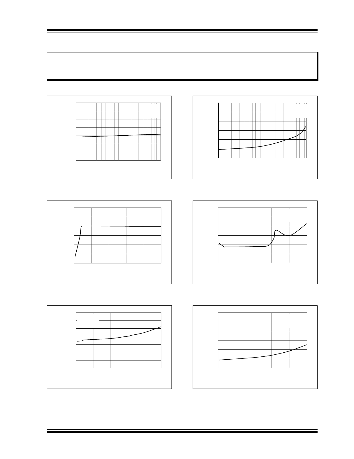
2.0
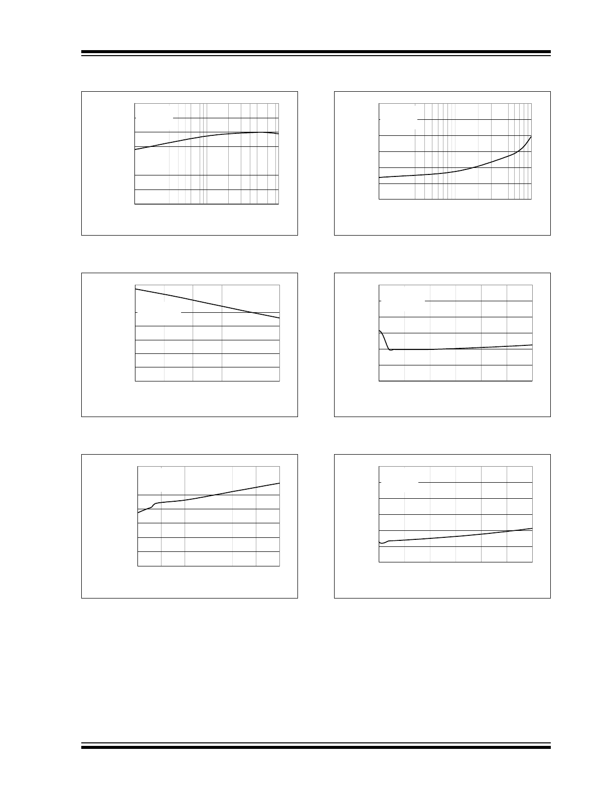
TYPICAL PERFORMANCE CURVES
NOTE: Unless otherwise indicated, V
DD
= [V
REG
(typ.) + 1V], I
OUT
= 10 mA and T
A
= +25°C, Constant-voltage mode.
FIGURE 2-1:
Battery Regulation Voltage
(V
BAT
) vs. Charge Current (I
OUT
).
FIGURE 2-2:
Battery Regulation Voltage
(V
BAT
) vs. Supply Voltage (V
DD
).
FIGURE 2-3:
Battery Regulation Voltage
(V
BAT
) vs. Supply Voltage (V
DD
).
FIGURE 2-4:
Supply Current (I
SS
) vs.
Charge Current (I
OUT
).
FIGURE 2-5:
Supply Current (I
SS
) vs.
Supply Voltage (V
DD
).
FIGURE 2-6:
Supply Current (I
SS
) vs.
Supply Voltage (V
DD
).
Note:
The graphs and tables provided following this note are a statistical summary based on a limited number of
samples and are provided for informational purposes only. The performance characteristics listed herein
are not tested or guaranteed. In some graphs or tables, the data presented may be outside the specified
operating range (e.g., outside specified power supply range) and therefore outside the warranted range.
4.193
4.195
4.197
4.199
4.201
4.203
4.205
4.207
10
100
1000
Charge Current (mA)
B
atte
ry R
egu
latio
n
V
o
ltage
(V
)
MCP73861/3
V
SET
= V
DD
V
DD
= 5.2V
3.80
3.90
4.00
4.10
4.20
4.30
4.40
4.5
6.0
7.5
9.0
10.5
12.0
Supply Voltage (V)
B
a
tter
y
R
e
gulation Voltage
(V
)
MCP73861/3
V
SET
= V
DD
I
OUT
= 1000 mA
4.193
4.195
4.197
4.199
4.201
4.203
4.205
4.207
4.5
6.0
7.5
9.0
10.5
12.0
Supply Voltage (V)
B
a
tter
y
R
egulation Voltage
(V
)
MCP73861/3
V
SET
= V
DD
I
OUT
= 10 mA
0.40
0.50
0.60
0.70
0.80
0.90
1.00
10
100
1000
Charge Current (mA)
S
u
pp
ly
C
u
rr
en
t (m
A
)
MCP73861/3
V
SET
= V
DD
V
DD
= 5.2V
0.40
0.60
0.80
1.00
1.20
1.40
1.60
4.5
6.0
7.5
9.0
10.5
12.0
Supply Voltage (V)
Su
p
p
ly
Cu
rr
en
t (
m
A)
MCP73861/3
V
SET
= V
DD
I
OUT
= 1000 mA
0.40
0.50
0.60
0.70
0.80
0.90
1.00
4.5
6.0
7.5
9.0
10.5
12.0
Supply Voltage (V)
Su
p
p
ly
Cu
rr
en
t (
m
A)
MCP73861/3
V
SET
= V
DD
I
OUT
= 10 mA
MCP73861/2/3/4
DS21893F-page 8
2004-2013 Microchip Technology Inc.
NOTE: Unless otherwise indicated, V
DD
= [V
REG
(typ.) + 1V], I
OUT
= 10 mA and T
A
= +25°C, Constant-voltage mode.
FIGURE 2-7:
Output Leakage Current
(I
DISCHARGE
) vs. Battery Regulation Voltage
(V
BAT
).
FIGURE 2-8:
Thermistor Reference
Voltage (V
THREF
) vs. Supply Voltage (V
DD
).
FIGURE 2-9:
Thermistor Reference
Voltage (V
THREF
) vs. Thermistor Bias Current
(I
THREF
).
FIGURE 2-10:
Supply Current (I
SS
) vs.
Ambient Temperature (T
A
).
FIGURE 2-11:
Battery Regulation Voltage
(V
BAT
) vs. Ambient Temperature (T
A
).
FIGURE 2-12:
Thermistor Reference
Voltage (V
THREF
) vs. Ambient Temperature (T
A
).
0.00
0.05
0.10
0.15
0.20
0.25
0.30
0.35
0.40
0.45
2.0
2.4
2.8
3.2
3.6
4.0
4.4
Battery Regulation Voltage (V)
O
u
tput Leakage
C
u
rrent (µA
)
MCP73861/3
V
SET
= V
DD
V
DD
= V
SS
+25°C
-40°C
+85°C
2.500
2.510
2.520
2.530
2.540
2.550
4.5
6.0
7.5
9.0
10.5
12.0
Supply Voltage (V)
The
rm.
Re
fe
re
nc
e Vol
ta
g
e (V)
MCP73861/3
V
SET
= V
DD
I
THREF
= 100 µA
2.500
2.505
2.510
2.515
2.520
0
25
50
75
100 125 150 175 200
Therm. Bias Current (µA)
Therm. R
eference
V
o
lt
age (V)
MCP73861/3
V
SET
= V
DD
0.40
0.60
0.80
1.00
1.20
1.40
1.60
-4
0
-3
0
-2
0
-1
0
0
10
20
30
40
50
60
70
80
Ambient Temperature (°C)
S
u
ppl
y C
u
rre
nt
(
m
A
)
MCP73861/3
V
SET
= V
DD
I
OUT
= 10 mA
4.193
4.195
4.197
4.199
4.201
4.203
4.205
4.207
-4
0
-3
0
-2
0
-1
0
0
10
20
30
40
50
60
70
80
Ambient Temperature (°C)
B
at
te
ry R
e
gul
at
ion V
o
lt
ag
e (
V
)
MCP73861/3
V
SET
= V
DD
I
OUT
= 10 mA
2.500
2.505
2.510
2.515
2.520
-4
0
-3
0
-2
0
-1
0
0
10
20
30
40
50
60
70
80
Ambient Temperature (°C)
Therm
. Re
fere
nce V
o
lt
ag
e (V
)
MCP73861/3
V
SET
= V
DD
I
THREF
= 100 µA
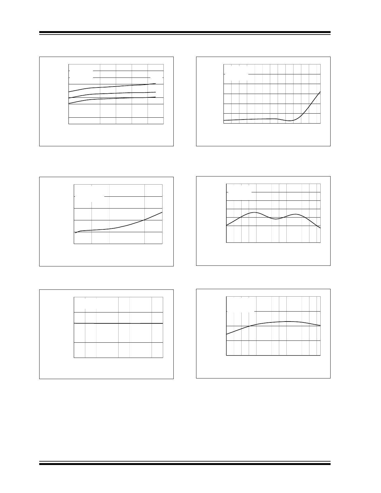
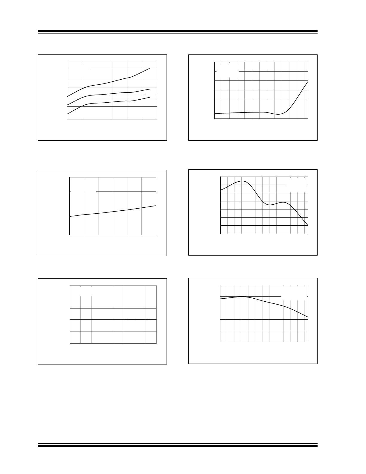
2004-2013 Microchip Technology Inc.
DS21893F-page 9
MCP73861/2/3/4
NOTE: Unless otherwise indicated, V
DD
= [V
REG
(typ.) + 1V], I
OUT
= 10 mA and T
A
= +25°C, Constant-voltage mode.
FIGURE 2-13:
Battery Regulation Voltage
(V
BAT
) vs. Charge Current (I
OUT
).
FIGURE 2-14:
Battery Regulation Voltage
(V
BAT
) vs. Supply Voltage (V
DD
).
FIGURE 2-15:
Battery Regulation Voltage
(V
BAT
) vs. Supply Voltage (V
DD
).
FIGURE 2-16:
Supply Current (I
SS
) vs.
Charge Current (I
OUT
).
FIGURE 2-17:
Supply Current (I
SS
) vs.
Supply Voltage (V
DD
).
FIGURE 2-18:
Supply Current (I
SS
) vs.
Supply Voltage (V
DD
).
8.393
8.395
8.397
8.399
8.401
8.403
8.405
8.407
10
100
1000
Charge Current (mA)
B
at
te
ry
R
egu
lation Voltage (V)
MCP73862/4
V
SET
= V
DD
V
DD
= 9.4V
8.393
8.395
8.397
8.399
8.401
8.403
8.405
8.407
10.0
10.4
10.8
11.2
11.6
12.0
Supply Voltage (V)
B
attery R
egula
tion Voltage (V)
MCP73862/4
V
SET
= V
DD
I
OUT
= 1000 mA
8.398
8.400
8.402
8.404
8.406
8.408
8.410
8.412
9.0
9.5
10.0
10.5
11.0
11.5
12.0
Supply Voltage (V)
B
att
er
y
R
eg
u
lati
on V
o
ltag
e (V
)
MCP73862/4
V
SET
= V
DD
I
OUT
= 10 mA
0.40
0.50
0.60
0.70
0.80
0.90
1.00
10
100
1000
Charge Current (mA)
S
uppl
y C
u
rrent
(
m
A
)
MCP73862/4
V
SET
= V
DD
V
DD
= 9.4V
0.40
0.60
0.80
1.00
1.20
1.40
1.60
9.0
9.5
10.0
10.5
11.0
11.5
12.0
Supply Voltage (V)
S
uppl
y C
u
rrent
(
m
A
)
MCP73862/4
V
SET
= V
DD
I
OUT
= 1000 mA
0.40
0.50
0.60
0.70
0.80
0.90
1.00
9.0
9.5
10.0
10.5
11.0
11.5
12.0
Supply Voltage (V)
S
uppl
y C
u
rre
nt
(
m
A
)
MCP73862/4
V
SET
= V
DD
I
OUT
= 10 mA
MCP73861/2/3/4
DS21893F-page 10
2004-2013 Microchip Technology Inc.
NOTE: Unless otherwise indicated, V
DD
= [V
REG
(typ.) + 1V], I
OUT
= 10 mA and T
A
= +25°C, Constant-voltage mode.
FIGURE 2-19:
Output Leakage Current
(I
DISCHARGE
) vs. Battery Regulation Voltage
(V
BAT
).
FIGURE 2-20:
Thermistor Reference
Voltage (V
THREF
) vs. Supply Voltage (V
DD
).
FIGURE 2-21:
Thermistor Reference
Voltage (V
THREF
) vs. Thermistor Bias Current
(I
THREF
).
FIGURE 2-22:
Supply Current (I
SS
) vs.
Ambient Temperature (T
A
).
FIGURE 2-23:
Battery Regulation Voltage
(V
BAT
) vs. Ambient Temperature (T
A
).
FIGURE 2-24:
Thermistor Reference
Voltage (V
THREF
) vs. Ambient Temperature (T
A
).
0.00
0.05
0.10
0.15
0.20
0.25
0.30
0.35
0.40
0.45
4.0
4.8
5.6
6.4
7.2
8.0
8.8
Battery Regulation Voltage (V)
Out
put
Leakag
e C
u
rr
ent
(µA
)
MCP73862/4
V
SET
= V
DD
V
DD
= V
SS
+25°C
-40°C
+85°C
2.530
2.540
2.550
2.560
2.570
9.0
9.5
10.0
10.5
11.0
11.5
12.0
Supply Voltage (V)
The
rm.
Re
fe
re
nc
e Vol
ta
g
e (V)
MCP73862/4
V
SET
= V
DD
I
THREF
= 100 µA
2.540
2.542
2.544
2.546
2.548
2.550
0
25
50
75
100 125 150 175 200
Thermistor Bias Current (µA)
Ther
m
. R
efer
ence
V
o
lta
g
e (V
)
MCP73862/4
V
SET
= V
DD
0.40
0.60
0.80
1.00
1.20
1.40
1.60
-4
0
-3
0
-2
0
-1
0
0
10
20
30
40
50
60
70
80
Ambient Temperature (°C)
Su
p
p
ly Cu
rr
en
t (m
A)
MCP73862/4
V
SET
= V
DD
I
OUT
= 10 mA
8.386
8.390
8.394
8.398
8.402
8.406
8.410
8.414
-40
-30
-20
-10
0
10
20
30
40
50
60
70
80
Ambient Temperature (°C)
B
attery R
egulation Voltag
e (V)
MCP73862/4
V
SET
= V
DD
I
OUT
= 10 mA
2.530
2.534
2.538
2.542
2.546
2.550
-40
-30
-20
-10
0
10
20
30
40
50
60
70
80
Ambient Temperature (°C)
Th
er
m
. R
efer
ence
V
o
lt
age (
V
)
MCP73862/4
V
SET
= V
DD
I
THREF
= 100 µA