
© 2002-2012 Microchip Technology Inc.
DS21714G-page 1
MCP6546/6R/6U/7/8/9
Features
• Low Quiescent Current: 600 nA/Comparator (typical)
• Rail-to-Rail Input: V
SS
- 0.3V to V
DD
+ 0.3V
• Open-Drain Output: V
OUT
≤ 10V
•
Propagation Delay: 4 µs (typical, 100 mV
Overdrive)
• Wide Supply Voltage Range: 1.6V to 5.5V
• Single Available in SOT-23-5, SC-70-5* Packages
• Available in Single, Dual and Quad
• Chip Select (CS) with MCP6548
• Low Switching Current
• Internal Hysteresis: 3.3 mV (typical)
• Temperature Range:
- Industrial: -40°C to +85°C
- Extended: -40°C to +125°C
Typical Applications
• Laptop Computers
• Mobile Phones
• Metering Systems
• Hand-held Electronics
• RC Timers
• Alarm and Monitoring Circuits
• Windowed Comparators
• Multi-vibrators
Related Devices
• CMOS/TTL-Compatible Output: MCP6541/2/3/4
Description
The Microchip Technology Inc. MCP6546/6R/6U/7/8/9
family of comparators, is offered in single (MCP6546,
MCP6546R, MCP6546U), single with chip select (CS)
(MCP6548), dual (MCP6547) and quad (MCP6549)
configurations. The outputs are open-drain and are
capable of driving heavy DC or capacitive loads.
These comparators are optimized for low power,
single-supply application with greater than rail-to-rail
input operation. The output limits supply current surges
and dynamic power consumption while switching. The
open-drain output of the MCP6546/6R/6U/7/8/9 family
can be used as a level-shifter for up to 10V using a pull-
up resistor. It can also be used as a wired-OR logic.
The internal Input hysteresis eliminates output switch-
ing due to internal noise voltage, reducing current draw.
These comparators operate with a single-supply
voltage as low as 1.6V and draw a quiescent current of
less than 1 µA/comparator.
The related MCP6541/2/3/4 family of comparators from
Microchip has a push-pull output that supports rail-to-
rail output swing and interfaces with CMOS/TTL logic.
* SC-70-5 E-Temp parts are not available at this
release of the data sheet.
MCP6546U SOT-23-5 is E-Temp only.
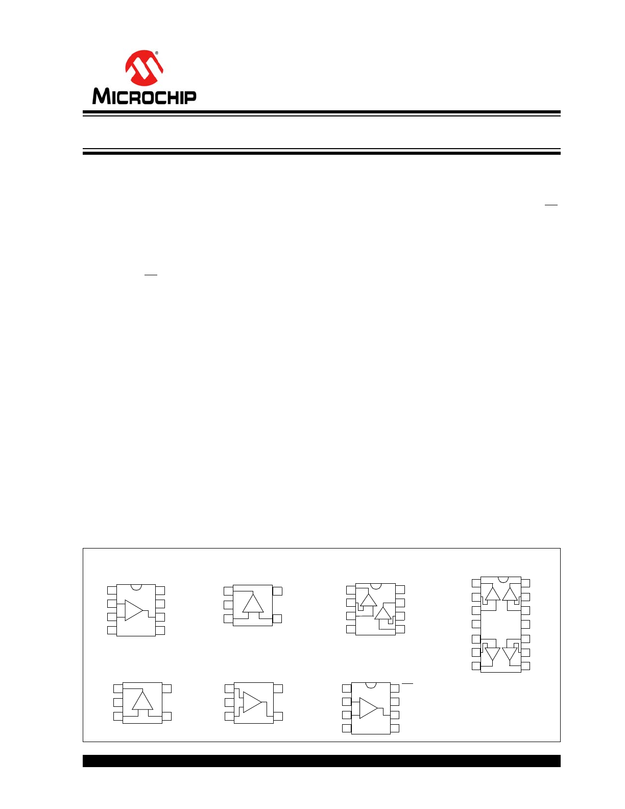
Package Types
V
IN
+
V
IN
–
MCP6546
V
SS
V
DD
OUT
1
2
3
4
8
7
6
5
-
+
NC
NC
NC
PDIP, SOIC, MSOP
4
1
2
3
-
+
5
SOT-23-5
V
DD
OUT
V
IN
+
V
SS
V
IN
–
MCP6546R
MCP6547
V
INA
+
V
INA
–
V
SS
1
2
3
4
8
7
6
5
-
OUTA
+ -
+
V
DD
OUTB
V
INB
–
V
INB
+
V
IN
+
V
IN
–
MCP6548
V
SS
V
DD
OUT
1
2
3
4
8
7
6
5
-
+
NC
CS
NC
PDIP, SOIC, MSOP
PDIP, SOIC, MSOP
MCP6549
V
INA
+
V
INA
–
V
SS
1
2
3
4
14
13
12
11
-
OUTA
+ -
+
V
DD
OUTD
V
IND
–
V
IND
+
10
9
8
5
6
7
OUTB
V
INB
–
V
INB
+
V
INC
+
V
INC
–
OUTC
+
-
-
+
PDIP, SOIC, TSSOP
4
1
2
3
-
+
5
SC-70-5, SOT23-5
V
SS
OUT
V
IN
+
V
DD
V
IN
–
MCP6546
4
1
2
3
5
SC-70-5, SOT-23-5
V
SS
V
IN
+
V
IN
–
V
DD
OUT
MCP6546U
-
+
Open-Drain Output Sub-Microamp Comparators
MCP6546/6R/6U/7/8/9
DS21714G-page 2
© 2002-2012 Microchip Technology Inc.
1.0
ELECTRICAL
CHARACTERISTICS
Absolute Maximum Ratings †
V
DD
- V
SS
.........................................................................7.0V
Open-Drain Output.............................................. V
SS
+ 10.5V
Analog Input (V
IN
+, V
IN
-)††............. V
SS
- 1.0V to V
DD
+ 1.0V
All Other Inputs and Outputs ......... V
SS
– 0.3V to V
DD
+ 0.3V
Difference Input Voltage ...................................... |V
DD
– V
SS
|
Output Short-Circuit Current .................................continuous
Current at Input Pins ....................................................±2 mA
Current at Output and Supply Pins ............................±30 mA
Storage Temperature.....................................-65°C to +150°C
Maximum Junction Temperature (T
J
) .......................... +150°C
ESD Protection on All Pins:
(HBM;MM) .....................................2 kV;200V (MCP6546U)
(HBM;MM) ................................ 4 kV; 200V (all other parts)
† Notice: Stresses above those listed under “Absolute
Maximum Ratings” may cause permanent damage to
the device. This is a stress rating only, and functional
operation of the device, at those or any other conditions
above those indicated in the operational listings of this
specification, is not implied. Exposure to maximum rat-
ing conditions for extended periods may affect device
reliability.
†† See
Section 4.1.2 “Input Voltage and Current
Limits”
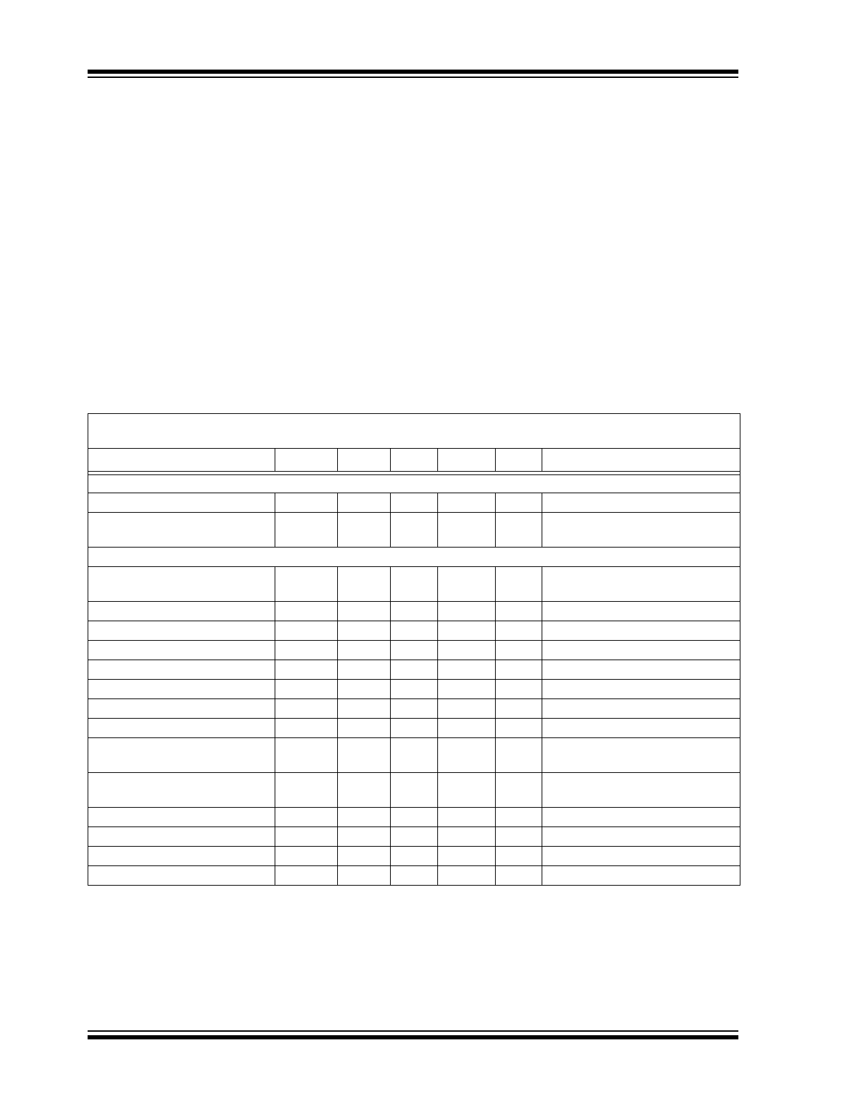
DC CHARACTERISTICS
Electrical Specifications: Unless otherwise indicated, V
DD
= +1.6V to +5.5V, V
SS
= GND, T
A
= 25°C, V
IN
+ = V
DD
/2,
V
IN
– = V
SS
, R
PU
= 2.74 k
Ω to V
PU
= V
DD
(Refer to
Figure 1-3
).
Parameters
Sym
Min
Typ
Max
Units
Conditions
Power Supply
Supply Voltage
V
DD
1.6
—
5.5
V
V
PU
≥ V
DD
Quiescent Current
(per comparator)
I
Q
0.3
0.6
1
µA
I
OUT
= 0
Input
Input Voltage Range
V
CMR
V
SS
−
0.3
—
V
DD
+ 0.3
V
Common Mode Rejection Ratio
CMRR
55
70
—
dB
V
DD
= 5V, V
CM
= -0.3V to 5.3V
Common Mode Rejection Ratio
CMRR
50
65
—
dB
V
DD
= 5V, V
CM
= 2.5V to 5.3V
Common Mode Rejection Ratio
CMRR
55
70
—
dB
V
DD
= 5V, V
CM
= -0.3V to 2.5V
Power Supply Rejection Ratio
PSRR
63
80
—
dB
V
CM
= V
SS
Input Offset Voltage
V
OS
-7.0
±1.5
+7.0
mV
V
CM
= V
SS
(
Note 1
)
Drift with Temperature
ΔV
OS
/
ΔT
A
—
±3
—
µV/°C T
A
= -40°C to +125°C, V
CM
= V
SS
Input Hysteresis Voltage
V
HYST
1.5
3.3
6.5
mV
V
CM
= V
SS
(
Note 1
)
Linear Temp. Co.
TC
1
—
6.7
—
µV/°C T
A
= -40°C to +125°C, V
CM
= V
SS
(
Note 2
)
Quadratic Temp. Co.
TC
2
—
-0.035
—
µV/°C
2
T
A
= -40°C to +125°C, V
CM
= V
SS
(
Note 2
)
Input Bias Current
I
B
—
1
—
pA
V
CM
=
V
SS
At Temperature (I-Temp parts)
I
B
—
25
100
pA
T
A
= +85°C, V
CM
= V
SS
(
Note 3
)
At Temperature (E-Temp parts)
I
B
—
1200
5000
pA
T
A
= +125°C, V
CM
= V
SS
(
Note 3
)
Input Offset Current
I
OS
—
±1
—
pA
V
CM
=
V
SS
Note 1:
The input offset voltage is the center of the input-referred trip points. The input hysteresis is the difference
between the input-referred trip points.
2:
V
HYST
at differential temperatures is estimated using:
V
HYST
(T
A
) = V
HYST
+ (T
A
-25°C) TC
1
+ (T
A
- 25°C)
2
TC
2
.
3:
Input bias current at temperature is not tested for the SC-70-5 package.
4:
Do not short the output above V
SS
+ 10V. Limit the output current to Absolute Maximum Rating of 30 mA.
The minimum V
PU
test limit was V
DD
before Dec. 2004 (week code 52).
© 2002-2012 Microchip Technology Inc.
DS21714G-page 3
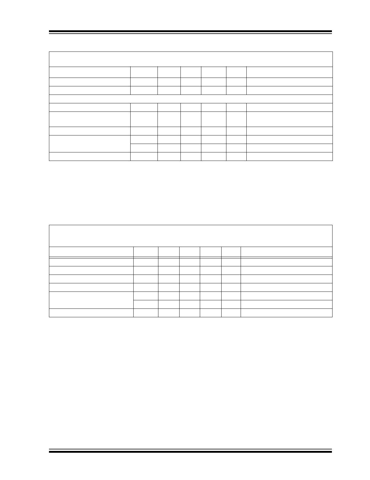
MCP6546/6R/6U/7/8/9
Common Mode Input Impedance
Z
CM
—
10
13
||4
—
Ω||pF
Differential Input Impedance
Z
DIFF
—
10
13
||2
—
Ω||pF
Open-Drain Output
Output Pull-Up Voltage
V
PU
1.6
—
10
V
(
Note 4
)
High-Level Output Current
I
OH
-100
—
—
nA
V
DD
= 1.6V to 5.5V, V
PU
= 10V
(
Note 4
)
Low-Level Output Voltage
V
OL
V
SS
—
V
SS
+ 0.2
V
I
OUT
= 2 mA, V
PU
= V
DD
= 5V
Short-Circuit Current
I
SC
—
±1.5
—
mA
V
PU
= V
DD
= 1.6V (
Note 4
)
I
SC
–
30
—
mA
V
PU
= V
DD
= 5.5V (
Note 4
)
Output Pin Capacitance
C
OUT
—
8
—
pF
AC CHARACTERISTICS
Electrical Specifications: Unless otherwise indicated, V
DD
= +1.6V to +5.5V, V
SS
= GND, T
A
= 25°C, V
IN
+ = V
DD
/2,
Step = 200 mV, Overdrive = 100 mV, R
PU
= 2.74 k
Ω to V
PU
= V
DD
, and C
L
= 36 pF
(Refer to
Figure 1-2
and
Figure 1-3
).
Parameters
Sym
Min
Typ
Max
Units
Conditions
Fall Time
t
F
—
0.7
—
µs
(
Note 1
)
Propagation Delay (High-to-Low)
t
PHL
—
4.0
8.0
µs
Propagation Delay (Low-to-High)
t
PLH
—
3.0
8.0
µs
(
Note 1
)
Propagation Delay Skew
t
PDS
—
-1.0
—
µs
(
Notes 1
and
2
)
Maximum Toggle Frequency
f
MAX
—
225
—
kHz
V
DD
= 1.6V
f
MAX
—
165
—
kHz
V
DD
= 5.5V
Input Noise Voltage
E
ni
—
200
—
µV
P-P
10 Hz to 100 kHz
Note 1:
t
R
and t
PLH
depend on the load (R
L
and C
L
); these specifications are valid for the indicated load only.
2:
Propagation Delay Skew is defined as: t
PDS
= t
PLH
- t
PHL
.
DC CHARACTERISTICS (CONTINUED)
Electrical Specifications: Unless otherwise indicated, V
DD
= +1.6V to +5.5V, V
SS
= GND, T
A
= 25°C, V
IN
+ = V
DD
/2,
V
IN
– = V
SS
, R
PU
= 2.74 k
Ω to V
PU
= V
DD
(Refer to
Figure 1-3
).
Parameters
Sym
Min
Typ
Max
Units
Conditions
Note 1:
The input offset voltage is the center of the input-referred trip points. The input hysteresis is the difference
between the input-referred trip points.
2:
V
HYST
at differential temperatures is estimated using:
V
HYST
(T
A
) = V
HYST
+ (T
A
-25°C) TC
1
+ (T
A
- 25°C)
2
TC
2
.
3:
Input bias current at temperature is not tested for the SC-70-5 package.
4:
Do not short the output above V
SS
+ 10V. Limit the output current to Absolute Maximum Rating of 30 mA.
The minimum V
PU
test limit was V
DD
before Dec. 2004 (week code 52).
MCP6546/6R/6U/7/8/9
DS21714G-page 4
© 2002-2012 Microchip Technology Inc.
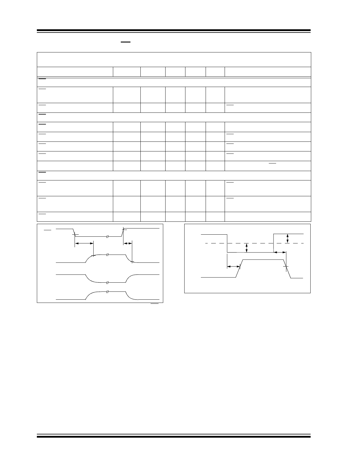
FIGURE 1-1:
Timing Diagram for the CS
pin on the MCP6548.
FIGURE 1-2:
Propagation Delay Timing
Diagram.
MCP6548 CHIP SELECT (CS) CHARACTERISTICS
Electrical Specifications: Unless otherwise indicated, V
DD
= +1.6V to +5.5V, V
SS
= GND, T
A
= 25°C, V
IN
+ = V
DD
/2,
V
IN
– = V
SS
, R
PU
= 2.74 k
Ω to V
PU
= V
DD
, and C
L
= 36 pF (Refer to
Figures 1-1
and
1-3
).
Parameters
Sym
Min
Typ
Max
Units
Conditions
CS Low Specifications
CS Logic Threshold, Low
V
IL
V
SS
—
0.2
V
DD
V
CS Input Current, Low
I
CSL
—
5
—
pA
CS = V
SS
CS High Specifications
CS Logic Threshold, High
V
IH
0.8 V
DD
—
V
DD
V
CS Input Current, High
I
CSH
—
1
—
pA
CS = V
DD
CS Input High, V
DD
Current
I
DD
—
18
—
pA
CS = V
DD
CS Input High, GND Current
I
SS
—
-20
—
pA
CS = V
DD
Comparator Output Leakage
I
O(LEAK)
—
1
—
pA
V
OUT
= V
SS
+10V, CS = V
DD
CS Dynamic Specifications
CS Low to Comparator Output
Low Turn-on Time
t
ON
—
2
50
ms
CS = 0.2V
DD
to V
OUT
= V
DD
/2,
V
IN
– = V
DD
CS High to Comparator Output
High Z Turn-off Time
t
OFF
—
10
—
µs
CS = 0.8V
DD
to V
OUT
= V
DD
/2,
V
IN
– = V
DD
CS Hysteresis
V
CS_HYST
—
0.6
—
V
V
DD
= 5V
V
IL
High-Z
t
ON
V
IH
CS
t
OFF
V
OUT
-20 pA (typ.)
High-Z
I
SS
I
CS
-20 pA (typ.)
-0.6 µA (typ.)
1 pA (typ.)
1 pA (typ.)
5 pA (typ.)
V
OL
t
PLH
V
OUT
V
IN
–
100 mV
100 mV
t
PHL
V
OL
V
IN
+ = V
DD
/2
V
OH
© 2002-2012 Microchip Technology Inc.
DS21714G-page 5
MCP6546/6R/6U/7/8/9
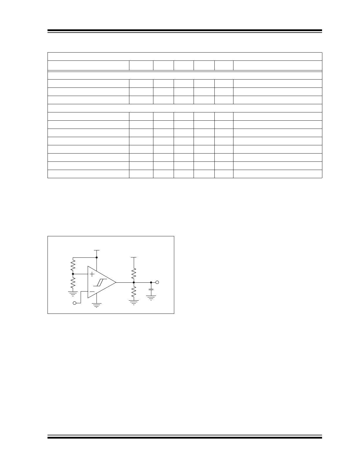
1.1
Test Circuit Configuration
This test circuit configuration is used to determine the
AC and DC specifications.
FIGURE 1-3:
AC and DC Test Circuit for
the Open-Drain Output Comparators.
TEMPERATURE CHARACTERISTICS
Electrical Specifications: Unless otherwise indicated, V
DD
= +1.6V to +5.5V and V
SS
= GND.
Parameters
Sym
Min
Typ
Max
Units
Conditions
Temperature Ranges
Specified Temperature Range
T
A
-40
—
+85
°C
Operating Temperature Range
T
A
-40
—
+125
°C
Note
Storage Temperature Range
T
A
-65
—
+150
°C
Thermal Package Resistances
Thermal Resistance, 5L-SC-70
θ
JA
—
331
—
°C/W
Thermal Resistance, 5L-SOT-23
θ
JA
—
220.7
—
°C/W
Thermal Resistance, 8L-MSOP
θ
JA
—
211
—
°C/W
Thermal Resistance, 8L-PDIP
θ
JA
—
89.3
—
°C/W
Thermal Resistance, 8L-SOIC
θ
JA
—
149.5
—
°C/W
Thermal Resistance, 14L-PDIP
θ
JA
—
70
—
°C/W
Thermal Resistance, 14L-SOIC
θ
JA
—
95.3
—
°C/W
Thermal Resistance, 14L-TSSOP
θ
JA
—
100
—
°C/W
Note:
The MCP6546/6R/6U/7/8/9 I-temp family operates over this extended temperature range, but with reduced
performance. In any case, the Junction Temperature (T
J
) must not exceed the absolute maximum
specification of +150°C.
V
DD
V
SS
= 0V
200 k
Ω
200 k
Ω
100 k
Ω
V
OUT
V
IN
= V
SS
36 pF
MCP654X
R
PU
=
V
PU
= V
DD
(2 mA)/ V
DD
MCP6546/6R/6U/7/8/9
DS21714G-page 6
© 2002-2012 Microchip Technology Inc.
2.0
TYPICAL PERFORMANCE CURVES
Note: Unless otherwise indicated, V
DD
= +1.6V to +5.5V, V
SS
= GND, T
A
= +25°C, V
IN
+ = V
DD
/2, V
IN
– = GND,
R
PU
= 2.74 k
Ω to V
PU
= V
DD
, and C
L
= 36 pF.
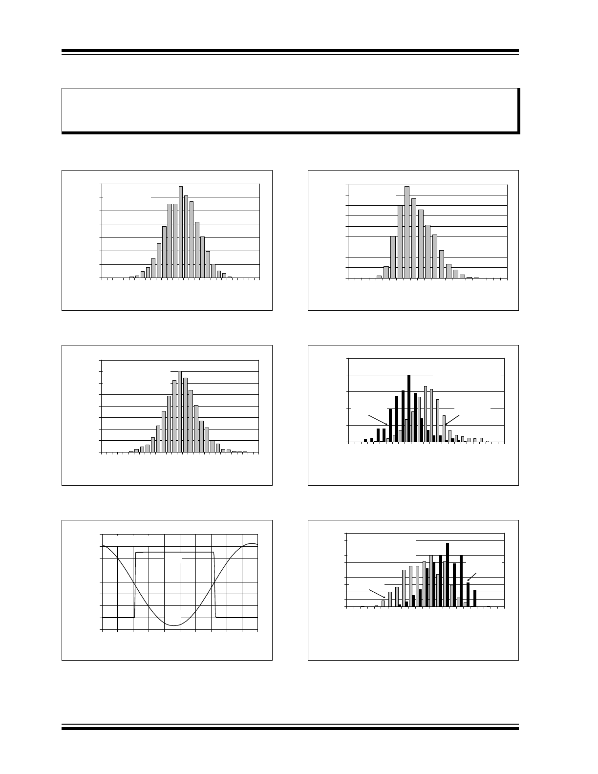
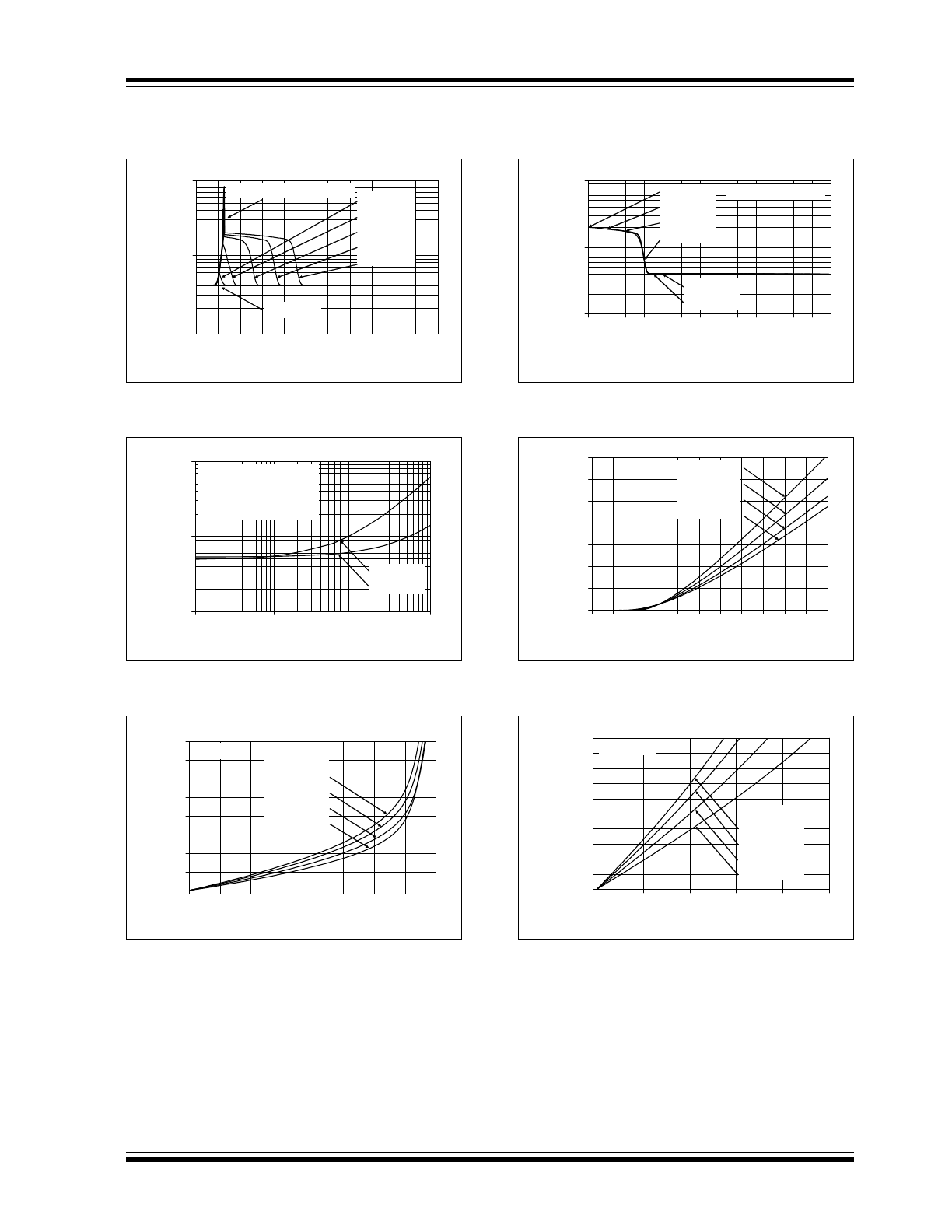
FIGURE 2-1:
Input Offset Voltage at
V
CM
= V
SS
.
FIGURE 2-2:
Input Offset Voltage Drift at
V
CM
= V
SS
.
FIGURE 2-3:
The MCP6546/6R/6U/7/8/9
Comparators Show No Phase Reversal.
FIGURE 2-4:
Input Hysteresis Voltage at
V
CM
= V
SS
.
FIGURE 2-5:
Input Hysteresis Voltage
Linear Temp. Co. (TC
1
) at V
CM
= V
SS
.
FIGURE 2-6:
Input Hysteresis Voltage
Quadratic Temp. Co. (TC
2
) at V
CM
= V
SS
.
Note:
The graphs and tables provided following this note are a statistical summary based on a limited number of
samples and are provided for informational purposes only. The performance characteristics listed herein
are not tested or guaranteed. In some graphs or tables, the data presented may be outside the specified
operating range (e.g., outside specified power supply range) and therefore outside the warranted range.
0%
2%
4%
6%
8%
10%
12%
14%
-7 -6 -5 -4 -3 -2 -1 0
1
2
3
4
5
6
7
Input Offset Voltage (mV)
P
e
rcent
a
ge
of
Occ
u
rr
en
ces
1200 Samples
V
CM
= V
SS
0%
2%
4%
6%
8%
10%
12%
14%
16%
-1
4
-1
2
-1
0
-8
-6
-4
-2
0
2
4
6
8
10
12
14
Input Offset Voltage Drift (µV/°C)
P
e
rcen
tag
e
o
f Oc
cur
re
n
ces
1200 Samples
V
CM
= V
SS
T
A
= -40°C to +125°C
-1
0
1
2
3
4
5
6
7
0
1
2
3
4
5
6
7
8
9
10
Time (1 ms/div)
In
ver
ti
n
g
I
npu
t,
O
u
tput
Vo
lt
a
g
e
(
V
)
V
OUT
V
IN
–
V
DD
= 5.5V
0%
2%
4%
6%
8%
10%
12%
14%
16%
18%
1.6 2.0 2.4 2.8 3.2 3.6 4.0 4.4 4.8 5.2 5.6 6.0
Input Hysteresis Voltage (mV)
P
e
rc
ent
a
ge of Occu
rr
en
ces
1200 Samples
V
CM
= V
SS
0%
5%
10%
15%
20%
25%
4.
6
5.
0
5.
4
5.
8
6.
2
6.
6
7.
0
7.
4
7.
8
8.
2
8.
6
9.
0
9.
4
Input Hysteresis Voltage –
Linear Temp. Co.; TC
1
(µV/°C)
P
e
rcent
a
ge
of
Occu
rr
en
ces
596 Samples
V
CM
= V
SS
T
A
= -40°C to +125°C
V
DD
= 1.6V
V
DD
= 5.5V
0%
2%
4%
6%
8%
10%
12%
14%
16%
18%
20%
-0.
060
-0.
056
-0.
052
-0.
048
-0.
044
-0.
040
-0.
036
-0.
032
-0.
028
-0.
024
-0.
020
-0.
016
Input Hysteresis Voltage –
Quadratic Temp. Co.; TC
2
(µV/°C
2
)
P
e
rcen
tage
of
Occu
rr
enc
e
s
596 Samples
V
CM
= V
SS
T
A
= -40°C to +125°C
V
DD
= 5.5V
V
DD
= 1.6V
© 2002-2012 Microchip Technology Inc.
DS21714G-page 7
MCP6546/6R/6U/7/8/9
Note: Unless otherwise indicated, V
DD
= +1.6V to +5.5V, V
SS
= GND, T
A
= +25°C, V
IN
+ = V
DD
/2, V
IN
– = GND,
R
PU
= 2.74 k
Ω to V
PU
= V
DD
, and C
L
= 36 pF.
FIGURE 2-7:
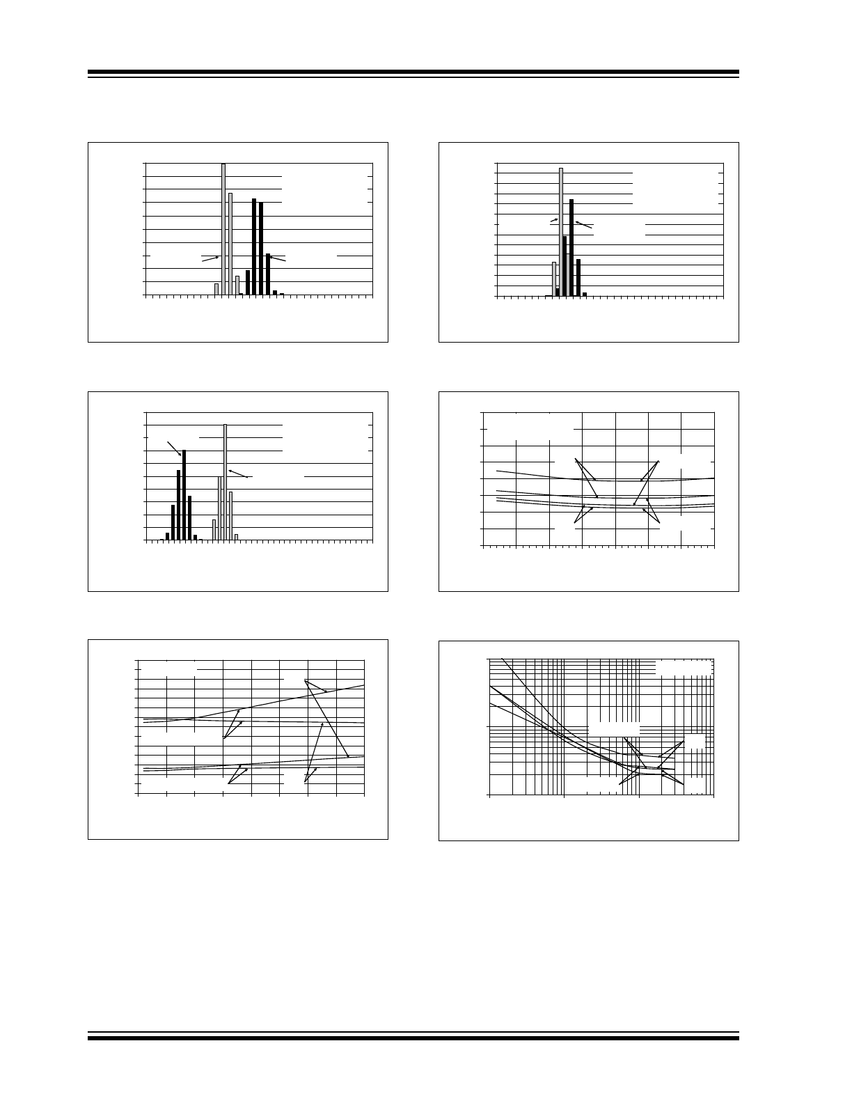
Input Offset Voltage vs.
Ambient Temperature at V
CM
= V
SS
.
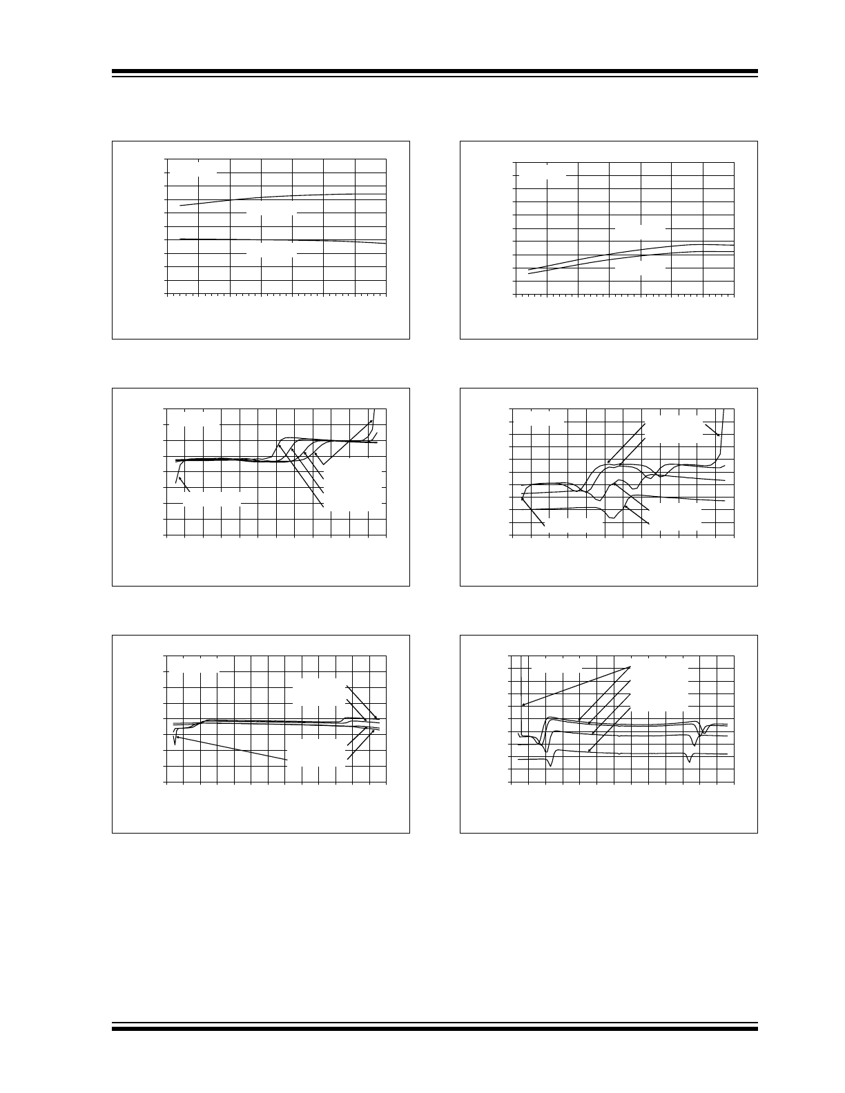
FIGURE 2-8:
Input Offset Voltage vs.
Common Mode Input Voltage at V
DD
= 1.6V.
FIGURE 2-9:
Input Offset Voltage vs.
Common Mode Input Voltage at V
DD
= 5.5V.
FIGURE 2-10:
Input Hysteresis Voltage vs.
Ambient Temperature at V
CM
= V
SS
.
FIGURE 2-11:
Input Hysteresis Voltage vs.
Common Mode Input Voltage at V
DD
= 1.6V.
FIGURE 2-12:
Input Hysteresis Voltage vs.
Common Mode Input Voltage at V
DD
= 5.5V.
-1.0
-0.8
-0.6
-0.4
-0.2
0.0
0.2
0.4
0.6
0.8
1.0
-50
-25
0
25
50
75
100
125
Ambient Temperature (°C)
Inp
u
t Of
fset
V
o
lt
age
(m
V
)
V
DD
= 1.6V
V
DD
= 5.5V
V
CM
= V
SS
-2.0
-1.5
-1.0
-0.5
0.0
0.5
1.0
1.5
2.0
-0
.4
-0
.2
0.0
0.2
0.4
0.6
0.8
1.0
1.2
1.4
1.6
1.8
2.0
Common Mode Input Voltage (V)
In
p
u
t Of
fset
V
o
lt
ag
e
(m
V
)
V
DD
= 1.6V
T
A
= +125°C
T
A
= +85°C
T
A
= +25°C
T
A
= -40°C
T
A
= +125°C
-2.0
-1.5
-1.0
-0.5
0.0
0.5
1.0
1.5
2.0
-0
.5
0.0
0.5
1.0
1.5
2.0
2.5
3.0
3.5
4.0
4.5
5.0
5.5
6.0
Common Mode Input Voltage (V)
Inpu
t Of
fse
t V
o
lt
age
(m
V
)
V
DD
= 5.5V
T
A
= +85°C
T
A
= +125°C
T
A
= -40°C
T
A
= +25°C
1.5
2.0
2.5
3.0
3.5
4.0
4.5
5.0
5.5
6.0
6.5
-50
-25
0
25
50
75
100
125
Ambient Temperature (°C)
In
p
u
t Hyste
res
is V
o
lt
ag
e
(m
V
)
V
DD
= 1.6V
V
DD
= 5.5V
V
CM
= V
SS
1.5
2.0
2.5
3.0
3.5
4.0
4.5
5.0
5.5
6.0
6.5
-0
.4
-0
.2
0.0
0.2
0.4
0.6
0.8
1.0
1.2
1.4
1.6
1.8
2.0
Common Mode Input Voltage (V)
Inp
u
t H
yste
res
is V
o
lt
ag
e (m
V
)
T
A
= +25°C
T
A
= -40°C
T
A
= +125°C
T
A
= +85°C
V
DD
= 1.6V
T
A
= +125°C
1.5
2.0
2.5
3.0
3.5
4.0
4.5
5.0
5.5
6.0
6.5
-0
.5
0.0
0.5
1.0
1.5
2.0
2.5
3.0
3.5
4.0
4.5
5.0
5.5
6.0
Common Mode Input Voltage (V)
In
put
H
yste
resi
s V
o
lt
age
(m
V
)
V
DD
= 5.5V
T
A
= +125°C
T
A
= +85°C
T
A
= +25°C
T
A
= -40°C
MCP6546/6R/6U/7/8/9
DS21714G-page 8
© 2002-2012 Microchip Technology Inc.
Note: Unless otherwise indicated, V
DD
= +1.6V to +5.5V, V
SS
= GND, T
A
= +25°C, V
IN
+ = V
DD
/2, V
IN
– = GND,
R
PU
= 2.74 k
Ω to V
PU
= V
DD
, and C
L
= 36 pF.
FIGURE 2-13:
CMRR,PSRR vs. Ambient
Temperature.
FIGURE 2-14:
Input Bias Current, Input
Offset Current vs. Ambient Temperature.
FIGURE 2-15:
Quiescent Current vs.
Common Mode Input Voltage at V
DD
= 1.6V.
FIGURE 2-16:
Input Bias Current, Input
Offset Current vs. Common Mode Input Voltage.
FIGURE 2-17:
Quiescent Current vs.
Power Supply Voltage.
FIGURE 2-18:
Quiescent Current vs.
Common Mode Input Voltage at V
DD
= 5.5V.
55
60
65
70
75
80
85
90
-50
-25
0
25
50
75
100
125
Ambient Temperature (°C)
CM
RR, PS
RR (
d
B)
Input Referred
PSRR, V
IN
+ = V
SS
, V
DD
= 1.6V to 5.5V
CMRR, V
IN
+ = -0.3 to 5.3V, V
DD
= 5.0V
0.1
1
10
100
1000
55
65
75
85
95
105
115
125
Ambient Temperature (°C)
Inpu
t B
ia
s
, O
ffse
t C
u
rr
e
nt
s
(p
A
)
I
B
| I
OS
|
V
DD
= 5.5V
V
CM
= V
DD
0.0
0.1
0.2
0.3
0.4
0.5
0.6
0.7
0.8
0.0
0.2
0.4
0.6
0.8
1.0
1.2
1.4
1.6
Common Mode Input Voltage (V)
Qu
iesce
nt C
u
rr
ent
per
C
o
m
p
ar
ato
r
(µA
)
V
DD
= 1.6V
Sweep V
IN
+, V
IN
– = V
DD
/2
Sweep V
IN
–, V
IN
+ = V
DD
/2
I
Q
does not include pull-up resistor current
0.1
1
10
100
1000
10000
0.0 0.5 1.0 1.5 2.0 2.5 3.0 3.5 4.0 4.5 5.0 5.5
Common Mode Input Voltage (V)
In
put
B
ias
, Of
fset
C
u
rr
e
nt
s
(A
)
V
DD
= 5.5V
100f
100p
1p
10p
1n
10n
I
B
, T
A
= +125°C
I
B
, T
A
= +85°C
I
OS
, T
A
= +125°C
I
OS
, T
A
= +85°C
0.0
0.1
0.2
0.3
0.4
0.5
0.6
0.7
0.0 0.5 1.0 1.5 2.0 2.5 3.0 3.5 4.0 4.5 5.0 5.5
Power Supply Voltage (V)
Qui
escen
t C
u
rr
e
nt
p
e
r C
o
m
p
ar
ato
r
(µ
A
)
T
A
= +125°C
T
A
= +85°C
T
A
= +25°C
T
A
= -40°C
0.0
0.1
0.2
0.3
0.4
0.5
0.6
0.7
0.8
0.0 0.5 1.0 1.5 2.0 2.5 3.0 3.5 4.0 4.5 5.0 5.5
Common Mode Input Voltage (V)
Qu
iesce
nt C
u
rr
ent
per
C
o
m
p
ar
ato
r
(µA
)
V
DD
= 5.5V
Sweep V
IN
+, V
IN
– = V
DD
/2
Sweep V
IN
–, V
IN
+ = V
DD
/2
I
Q
does not include pull-up resistor current
© 2002-2012 Microchip Technology Inc.
DS21714G-page 9
MCP6546/6R/6U/7/8/9
Note: Unless otherwise indicated, V
DD
= +1.6V to +5.5V, V
SS
= GND, T
A
= +25°C, V
IN
+ = V
DD
/2, V
IN
– = GND,
R
PU
= 2.74 k
Ω to V
PU
= V
DD
, and C
L
= 36 pF.
FIGURE 2-19:
Supply Current vs. Pull-Up
Voltage.
FIGURE 2-20:
Supply Current vs. Toggle
Frequency.
FIGURE 2-21:
Output Voltage Headroom
vs. Output Current at V
DD
= 1.6V.
FIGURE 2-22:
Supply Current vs. Pull-Up
to Supply Voltage Difference.
FIGURE 2-23:
Output Short Circuit Current
Magnitude vs. Power Supply Voltage.
FIGURE 2-24:
Output Voltage Headroom
vs. Output Current at V
DD
= 5.5V.
0.1
1
10
0
1
2
3
4
5
6
7
8
9
10 11
Pull-Up Voltage, V
PU
(V)
S
upp
ly
C
u
rr
ent
p
e
r C
o
m
p
ar
ato
r
(µA
)
V
DD
= 2.1V
V
DD
= 2.6V
V
DD
= 3.6V
V
DD
= 4.6V
V
DD
= 5.6V
I
DD
spike near V
PU
= 1.3V
V
DD
= 1.6V
0.1
1
10
0.1
1
10
100
Toggle Frequency (kHz)
Su
pp
ly
C
u
rr
e
nt
p
e
r C
o
m
p
ar
ato
r
(µ
A
)
V
DD
= 5.5V
V
DD
= 1.6V
100 mV Overdrive
V
CM
= V
DD
/2
I
DD
does not include
pull-up resistor current
0.0
0.1
0.2
0.3
0.4
0.5
0.6
0.7
0.8
0.0
0.2
0.4
0.6
0.8
1.0
1.2
1.4
1.6
Output Current (mA)
Out
put
V
o
lta
g
e H
ead
ro
om
(V
)
V
DD
= 1.6V
V
OL
–V
SS
:
T
A
= +125°C
T
A
= +85°C
T
A
= +25°C
T
A
= -40°C
0.1
1
10
-4 -3 -2 -1
0
1
2
3
4
5
6
7
8
9
Pull-up to Supply Voltage Difference,
V
PU
– V
DD
(V)
Su
pp
ly
C
u
rr
e
n
t
per
C
o
m
p
ar
at
or
(µ
A
)
V
DD
= 5.6V
V
DD
= 4.6V
V
DD
= 3.6V
V
DD
= 2.6V
V
PU
= 1.6V to 10.5V
V
DD
= 1.6V
V
DD
= 2.1V
0
5
10
15
20
25
30
35
0.0 0.5 1.0 1.5 2.0 2.5 3.0 3.5 4.0 4.5 5.0 5.5
Power Supply Voltage (V)
Ou
tp
ut
S
h
or
t C
ir
c
u
it C
u
rr
ent
Mag
n
it
ude
(m
A
)
T
A
= -40°C
T
A
= +25°C
T
A
= +85°C
T
A
= +125°C
0.0
0.1
0.2
0.3
0.4
0.5
0.6
0.7
0.8
0.9
1.0
0
5
10
15
20
25
Output Current (mA)
O
u
tput
V
o
lt
age
H
e
a
d
ro
om
(V
)
V
DD
= 5.5V
T
A
= +125°C
T
A
= +85°C
T
A
= +25°C
T
A
= -40°C
V
OL
– V
SS
:
MCP6546/6R/6U/7/8/9
DS21714G-page 10
© 2002-2012 Microchip Technology Inc.
Note: Unless otherwise indicated, V
DD
= +1.6V to +5.5V, V
SS
= GND, T
A
= +25°C, V
IN
+ = V
DD
/2, V
IN
– = GND,
R
PU
= 2.74 k
Ω to V
PU
= V
DD
, and C
L
= 36 pF.
FIGURE 2-25:
High-to-Low Propagation
Delay.
FIGURE 2-26:
Propagation Delay Skew.
FIGURE 2-27:
Propagation Delay vs.
Power Supply Voltage.
FIGURE 2-28:
Low-to-High Propagation
Delay.
FIGURE 2-29:
Propagation Delay vs.
Ambient Temperature.
FIGURE 2-30:
Propagation Delay vs. Input
Overdrive.
0%
5%
10%
15%
20%
25%
30%
35%
40%
45%
50%
0
1
2
3
4
5
6
7
8
High-to-Low Propagation Delay (µs)
P
e
rcen
tag
e
o
f O
ccur
re
nce
s
408 Samples
100 mV Overdrive
V
CM
= V
DD
/2
V
DD
= 5.5V
V
DD
= 1.6V
0%
5%
10%
15%
20%
25%
30%
35%
40%
45%
50%
-2
.0
-1
.6
-1
.2
-0
.8
-0
.4
0.0
0.4
0.8
1.2
1.6
2.0
Propagation Delay Skew (µs)
P
e
rcent
a
ge of
Occu
rr
en
ces
408 Samples
100 mV Overdrive
V
CM
= V
DD
/2
V
DD
= 1.6V
V
DD
= 5.5V
0
1
2
3
4
5
6
7
8
9
10
11
12
13
14
1.5
2.0
2.5
3.0
3.5
4.0
4.5
5.0
5.5
Power Supply Voltage (V)
P
ropag
a
ti
on D
e
lay (µs
)
V
CM
= V
DD
/2
t
PHL
10 mV Overdrive
100 mV Overdrive
t
PLH
0%
5%
10%
15%
20%
25%
30%
35%
40%
45%
50%
55%
60%
65%
0
1
2
3
4
5
6
7
8
Low-to-High Propagation Delay (µs)
P
e
rcen
tag
e
of
Occ
u
rr
en
ces
408 Samples
100 mV Overdrive
V
CM
= V
DD
/2
V
DD
= 5.5V
V
DD
= 1.6V
0
1
2
3
4
5
6
7
8
-50
-25
0
25
50
75
100
125
Ambient Temperature (°C)
P
ropag
a
ti
on D
e
lay (µs
)
100 mV Overdrive
V
CM
= V
DD
/2
t
PHL
t
PLH
V
DD
= 5.5V
V
DD
= 1.6V
1
10
100
1
10
100
1000
Input Overdrive (mV)
P
ropag
a
ti
on D
e
lay
(µ
s)
V
CM
= V
DD
/2
t
PLH
V
DD
= 5.5V
t
PHL
V
DD
= 1.6V