

2011-2016 Microchip Technology Inc.
DS20002284B-page 1
MCP16323
Features
• Up to 95% Typical Efficiency
• Input Voltage Range: 6.0V to 18V
• 3A Output Current
• Fixed Output Voltages: 0.9V, 1.5V, 1.8V, 2.5V,
3.3V, 5V with 2% Output Voltage Accuracy
• Adjustable Version Output Voltage Range:
0.9V to 5V with 1.5% Reference Voltage Accuracy
• Integrated N-Channel High-Side Switch: 180 mΩ
• Integrated N-Channel Low-Side Switch: 120 mΩ
• 1 MHz Fixed Frequency
• Low Device Shutdown Current
• Peak Current Mode Control
• Internal Compensation
• Stable with Ceramic Capacitors
• Internal Soft-Start
• Cycle-by-Cycle Peak Current Limit
• Undervoltage Lockout (UVLO): 5.75V
• Overtemperature Protection
• V
OUT
Overvoltage Protection
• V
OUT
Voltage Supervisor Reported at the PG Pin
• Available Package: QFN-16 (3x3 mm)
Applications
• PIC
®
/dsPIC
®
Microcontroller Bias Supply
• 12V Industrial Input DC-DC Conversion
• Set-Top Boxes
• DSL Cable Modems
• Automotive
• Wall Cube Regulation
• SLA Battery Powered Devices
• AC-DC Digital Control Power Source
• Power Meters
• Consumer
• Medical and Health Care
• Distributed Power Supplies
Description
The MCP16323 is a highly integrated, high-efficiency,
fixed frequency, synchronous step-down DC-DC
converter in a 16-pin QFN package that operates from
input voltages up to 18V. Integrated features include a
high-side and low-side N-Channel switch, fixed
frequency Peak Current Mode Control, internal
compensation, peak current limit, V
OUT
overvoltage
protection and overtemperature protection. Minimal
external components are necessary to develop a
complete synchronous step-down DC-DC converter
power supply.
High converter efficiency is achieved by integrating a
high-speed, current limited, low resistance, high-side
N-Channel MOSFET, as well as a high-speed, low-
resistance, low-side N-Channel MOSFET and
associated drive circuitry. High switching frequency
minimizes the size of the inductor and output capacitor,
resulting in a small solution size.
The MCP16323 device can supply 3A of continuous
current while regulating the output voltage from 0.9V to
5V. A high-performance peak current mode
architecture keeps the output voltage tightly regulated,
even during input voltage steps and output current
transient conditions that are common in power
supplies.
The regulator can be turned on and off with a logic level
signal applied to the EN input. The EN pin is internally
pulled up to a 4.2V reference and is rated for a
maximum of 6V. With EN low, typically 5 µA of current
is consumed from the input, making the part ideal for
power shedding and load distribution applications. The
PG output is an open-drain output pin used to interface
with other components of the system, and can be
pulled up to a maximum of 6V.
The output voltage can either be fixed at output
voltages of 0.9V, 1.5V, 1.8V, 2.5V, 3.3V, 5V or
adjustable using an external resistor divider. The
MCP16323 is offered in a 3x3 QFN-16 surface mount
package.
18V Input, 3A Output, High Efficiency Synchronous Buck Regulator
with Power Good Indication
Obsolete Device
For further designs, please refer to the MIC24046 Data Sheet
MCP16323
DS20002284B-page 2
2011-2016 Microchip Technology Inc.
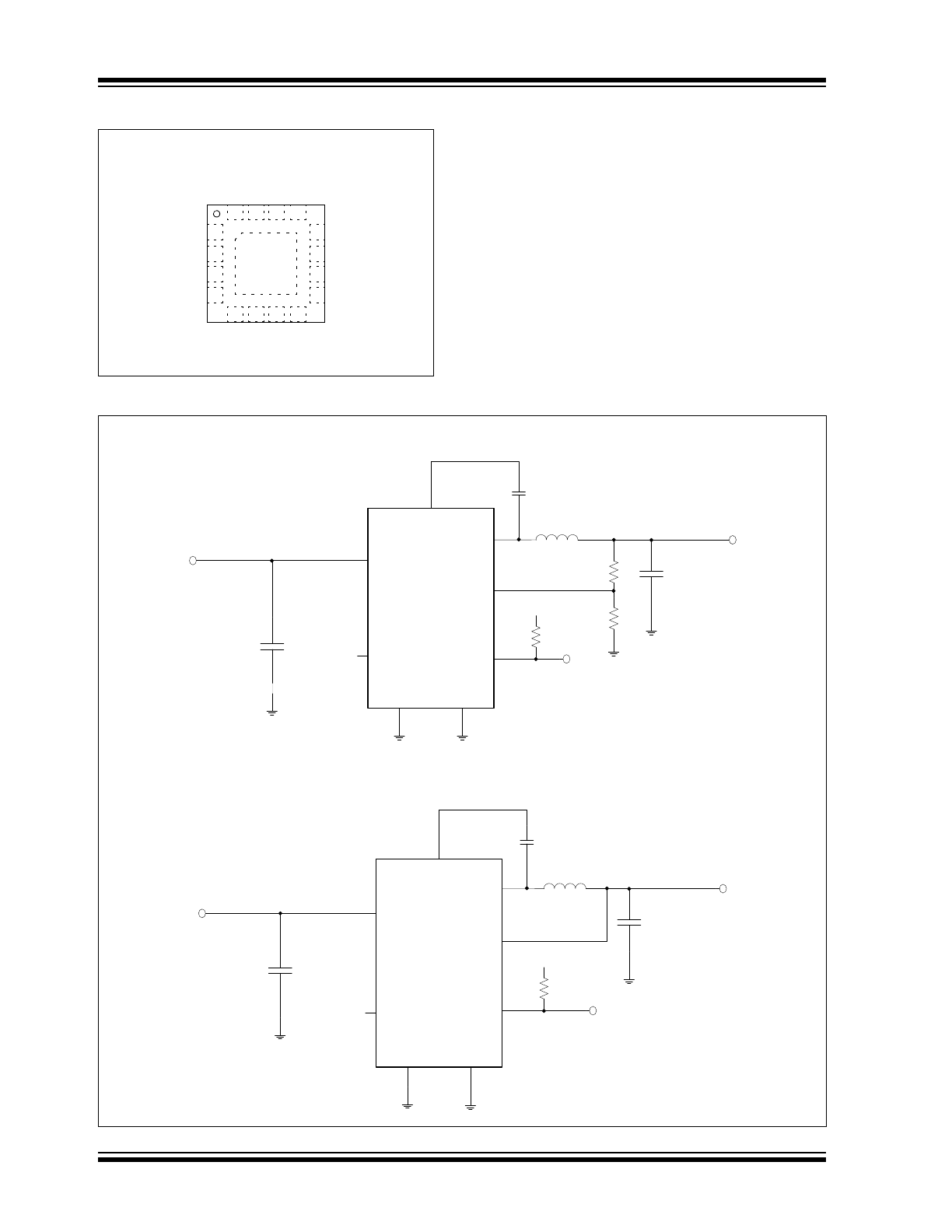
Package Type
Typical Applications
2
MCP16323
3x3 QFN*
V
IN
S
GND
SW
SW
V
IN
FB
BOOST
NC
NC
PG
EN
SW
P
GN
D
P
GN
D
SW
V
IN
EP
16
1
15 14 13
3
4
12
11
10
9
5
6
7
8
17
* Includes Exposed Thermal Pad (EP); see
Table 3-1
.
S
GND
P
GND
SW
V
FB
V
IN
EN
BOOST
V
IN
6.0V to 18V
C
BOOST
22 nF
L1
4.7 µH
C
IN
2x10 µF
C
OUT
2 x 22 µF
V
OUT
3.3V @ 3A
PG
V
OUT
10
kΩ
S
GND
P
GND
SW
V
FB
V
IN
EN
BOOST
V
IN
6.0V to 18V
C
BOOST
22 nF
L1
4.7 µH
C
IN
2x10 µF
C
OUT
2 x 22 µF
V
OUT
4.2V @ 3A
10
kΩ
36.5
kΩ
PG
V
OUT
10
kΩ
MCP
1
6
323
MC
P16
323
Typical Application with Fixed Output Voltage
Typical Application with Adjustable Output Voltage
2011-2016 Microchip Technology Inc.
DS20002284B-page 3
MCP16323
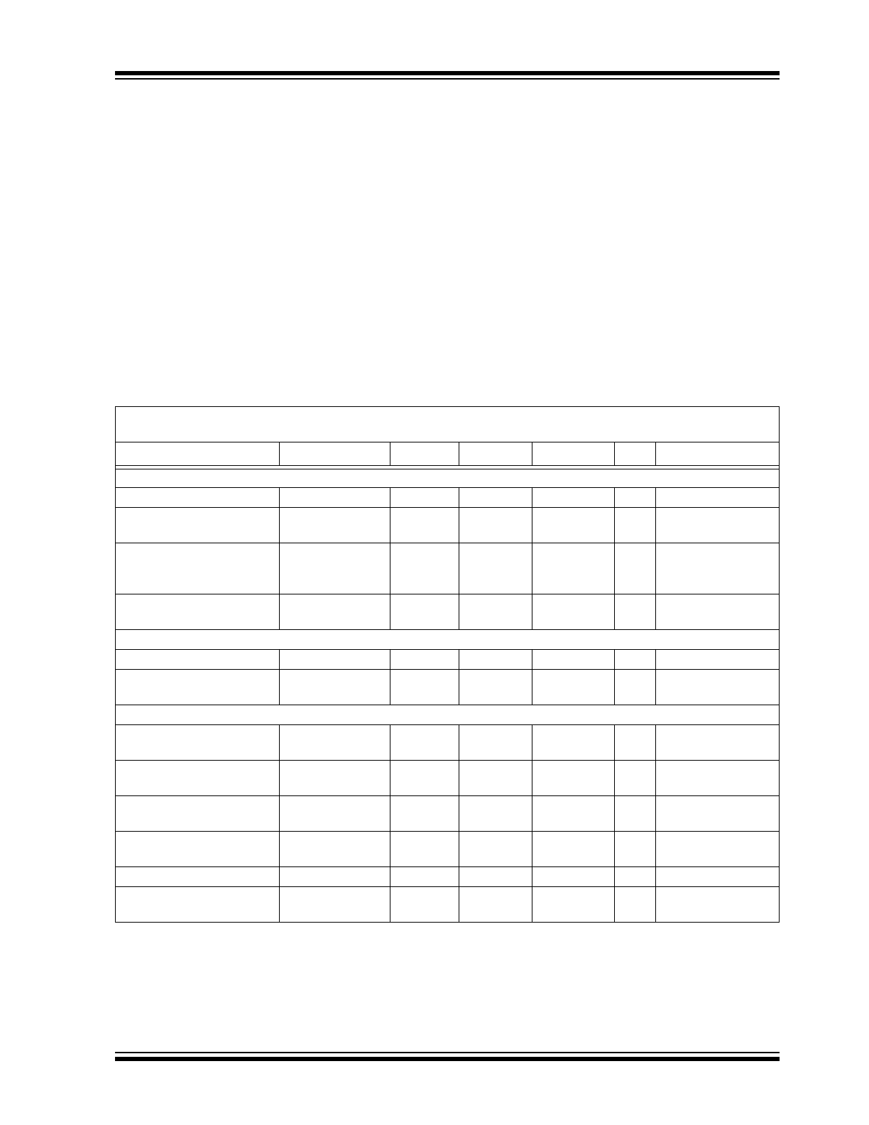
1.0
ELECTRICAL
CHARACTERISTICS
Absolute Maximum Ratings†
V
IN
....................................................................... -0.3V to 20V
SW ......................................................................... -1V to 20V
BOOST – GND ........................................... -0.3V to (V
IN
+6V)
EN,V
FB
, PG Voltage.............................................. -0.3V to 6V
Continuous Total Power Dissipation .......................................
...................................................See Thermal Characteristics
Storage Temperature ....................................-65°C to +150°C
Operating Junction Temperature...................-40°C to +125°C
ESD Protection On All Pins:
HBM ......................................................................... 3 kV
MM ..........................................................................200V
† Notice:
Stresses above those listed under “Absolute
Maximum Ratings” may cause permanent damage to
the device. This is a stress rating only and functional
operation of the device at those or any other conditions
above those indicated in the operational sections of this
specification is not intended. Exposure to maximum
rating conditions for extended periods may affect
device reliability.
DC CHARACTERISTICS
Electrical Characteristics:
Unless otherwise indicated, T
A
= +25°C, V
IN
= 12V, V
OUT
= 3.3V, I
OUT
= 300 mA,
L = 4.7 µH, C
OUT
= 2x22 µF, C
IN
= 2x10 µF. Boldface specifications apply over the T
J
range of -40°C to +125°C.
Parameters
Sym.
Min.
Typ.
Max.
Units Conditions
V
IN
Supply Voltage
Input Voltage
V
IN
6.0
—
18
V
Quiescent Current
(Switching)
I
Q
—
5.2
—
mA
I
OUT
= 0 mA
Quiescent Current
(Non-Switching)
I
Q
—
2.3
—
mA
Closed Loop in
Overvoltage
I
OUT
= 0 mA
Quiescent Current -
Shutdown
I
Q
—
5
10
µA
EN = 0
V
IN
Undervoltage Lockout
Undervoltage Lockout Start
UVLO
STRT
5.5
5.75
6.0
V
V
IN
Rising
Undervoltage Lockout
Hysteresis
UVLO
HYS
—
0.65
—
V
Non-Switching
Output Characteristics
Maximum Output Current
MCP16323
I
OUT
3
—
—
A
Note 2
Output Voltage Adjust
Range
V
OUT
0.9
—
5.0
V
Output Voltage Tolerance
in PWM Mode
V
OUT-PWM
V
OUT
- 2%
V
OUT
V
OUT
+ 2%
V
I
OUT
= 1A
Output Voltage Tolerance
in PFM Mode
V
OUT-PFM
V
OUT
- 1%
V
OUT
+ 1% V
OUT
+ 3.5%
V
I
OUT
= 0A
Feedback Voltage
V
FB
0.886
0.9
0.914
V
Feedback Reference
Tolerance
V
FB-TOL
-1.5
—
1.5
%
Note 1:
Regulator SW pin is forced off for 240 ns every eight cycles to ensure the BOOST cap is replenished.
2:
As a result of the maximum duty cycle limitations, 3A of output current for 5V output conditions may not
regulate the voltage. External component selection may have an impact on this. A minimum input voltage
of 6.5V is recommended.
MCP16323
DS20002284B-page 4
2011-2016 Microchip Technology Inc.
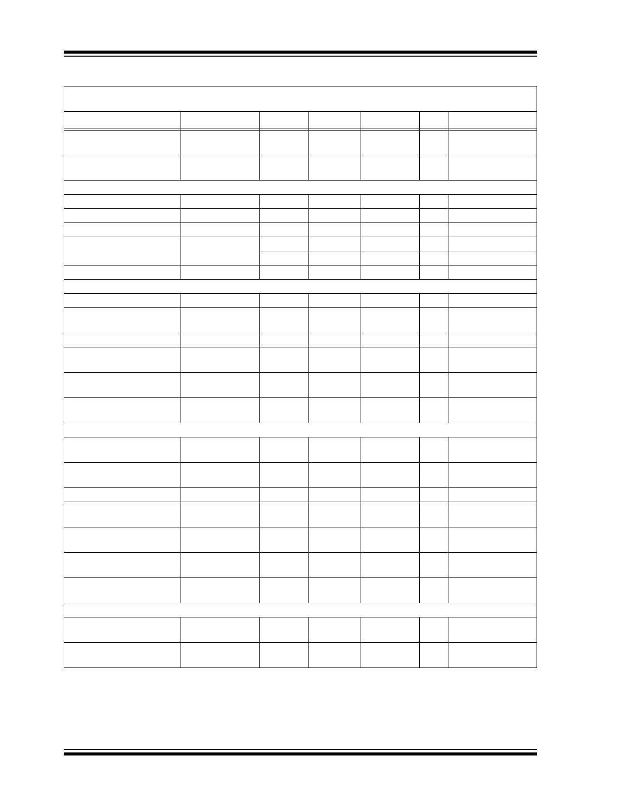
PFM Mode Feedback
Comparator Threshold
V
FB-PFM
—
V
OUT
+ 1%
—
V
Feedback Input Bias
Current
I
FB
—
100
—
nA
EN Input Characteristics
EN Input Logic High
V
IH
2.2
—
—
V
EN Input Logic Low
V
IL
—
—
0.8
V
EN Input Hysteresis
V
EN-HYST
—
480
—
mV
EN Input Leakage Current
I
ENLK
—
3.5
—
µA
V
EN
= 5V
—
-1.5
—
µA
V
EN
= 0V
Soft-Start Time
t
SS
—
4
—
ms
Switching Characteristics
Switching Frequency
f
SW
0.9
1
1.1
MHz Open Loop V
FB
Low
Maximum Duty Cycle
DC
MAX
95
97
99
%
Open Loop V
FB
Low
Note 1
Minimum Duty Cycle
—
7
—
%
NMOS Low-Side
Switch On Resistance
Low-Side R
DS(ON)
—
120
—
m
NMOS High-Side
Switch On Resistance
High-Side
R
DS(ON)
—
180
—
m
NMOS High-Side
Switch Current Limit
I
N(MAX)
3.4
3.8
4.4
A
MCP16323
PG Output Characteristics
PG Low-level
Output Voltage
PG
IL
—
—
0.01
V
I
PG
= -0.3 mA
PG High-Level Output
Leakage Current
I
PGLK
—
0.5
—
µA
V
PG
= 5V
PG Release Timer
t
PG
—
10
—
ms
V
OUT
Undervoltage
Threshold
V
OUT-UV
91% V
OUT
93% V
OUT
95% V
OUT
V
OUT
Undervoltage
Hysteresis
V
OUT-UV_HYST
—
1.5% V
OUT
—
V
OUT
Overvoltage Thresh-
old
V
OUT-OV
—
103% V
OU
T
—
V
OUT
Overvoltage
Hysteresis
V
OUT-OV_HYST
—
1% V
OUT
—
Thermal Characteristics
Thermal Shutdown
Die Temperature
T
SD
—
170
—
°C
Die Temperature
Hysteresis
T
SDHYS
—
10
—
°C
DC CHARACTERISTICS (CONTINUED)
Electrical Characteristics:
Unless otherwise indicated, T
A
= +25°C, V
IN
= 12V, V
OUT
= 3.3V, I
OUT
= 300 mA,
L = 4.7 µH, C
OUT
= 2x22 µF, C
IN
= 2x10 µF. Boldface specifications apply over the T
J
range of -40°C to +125°C.
Parameters
Sym.
Min.
Typ.
Max.
Units Conditions
Note 1:
Regulator SW pin is forced off for 240 ns every eight cycles to ensure the BOOST cap is replenished.
2:
As a result of the maximum duty cycle limitations, 3A of output current for 5V output conditions may not
regulate the voltage. External component selection may have an impact on this. A minimum input voltage
of 6.5V is recommended.
2011-2016 Microchip Technology Inc.
DS20002284B-page 5
MCP16323
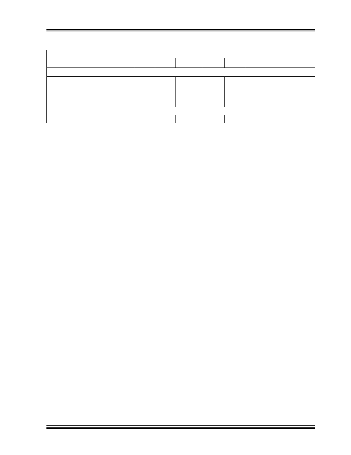
TABLE 1-1:
TEMPERATURE CHARACTERISTICS
Electrical Characteristics
Parameters
Sym
Min
Typ
Max
Units
Conditions
Temperature Ranges
Operating Junction Temperature
Range
T
J
-40
—
125
°C
Steady State
Storage Temperature Range
T
A
-65
—
150
°C
Maximum Junction Temperature
T
J
—
—
150
°C
Transient
Package Thermal Resistances
Thermal Resistance, 16L 3x3-QFN
JA
—
38.5
—
°C/W
Note 1:
Measured using a 4-layer FR4 Printed Circuit Board with a 13.5 in
2
, 1 oz internal copper ground plane.

MCP16323
DS20002284B-page 6
2011-2016 Microchip Technology Inc.
NOTES:
2011-2016 Microchip Technology Inc.
DS20002284B-page 7
MCP16323
2.0
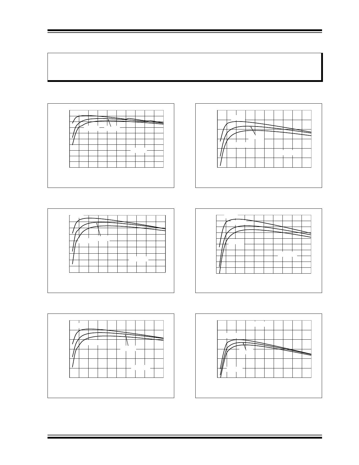
TYPICAL PERFORMANCE CURVES
Note:
Unless otherwise indicated, V
IN
= 12V, EN = Floating (internally pulled up), C
IN
= 20 µF, C
OUT
= 2x22 µF,
L = 4.7 µH (XAL6060-472MEB), I
LOAD
= 200 mA, T
A
= +25°C.
FIGURE 2-1:
5V V
OUT
Efficiency vs. I
OUT
.
FIGURE 2-2:
3.3V V
OUT
Efficiency vs.
I
OUT.
FIGURE 2-3:
2.5V V
OUT
Efficiency vs.
I
OUT.
FIGURE 2-4:
1.8V V
OUT
Efficiency vs.
I
OUT
.
FIGURE 2-5:
1.5V V
OUT
Efficiency vs.
I
OUT.
FIGURE 2-6:
0.9V V
OUT
Efficiency vs.
I
OUT.
Note:
The graphs and tables provided following this note are a statistical summary based on a limited number of
samples and are provided for informational purposes only. The performance characteristics listed herein
are not tested or guaranteed. In some graphs or tables, the data presented may be outside the specified
operating range (e.g., outside specified power supply range) and therefore outside the warranted range.
50
55
60
65
70
75
80
85
90
95
100
0.0
0.6
1.2
1.8
2.4
3.0
Efficiency
(%
)
I
OUT
(A)
V
IN
= 6V
V
IN
= 18V
V
IN
= 12V
V
OUT
= 5V
50
55
60
65
70
75
80
85
90
95
0
0.6
1.2
1.8
2.4
3
Efficiency
(%
)
I
OUT
(A)
V
IN
= 6V
V
IN
= 18V
V
IN
= 12V
V
OUT
= 3.3V
40
50
60
70
80
90
100
0
0.6
1.2
1.8
2.4
3
Efficiency
(%
)
I
OUT
(A)
V
IN
= 6V
V
IN
= 18V
V
IN
= 12V
V
OUT
= 2.5V
40
50
60
70
80
90
100
0
0.6
1.2
1.8
2.4
3
Efficiency
(%
)
I
OUT
(A)
V
IN
= 6V
V
IN
= 18V
V
IN
= 12V
V
OUT
= 1.8V
40
45
50
55
60
65
70
75
80
85
90
0
0.6
1.2
1.8
2.4
3
Efficiency
(%
)
I
OUT
(A)
V
IN
= 6V
V
IN
= 18V
V
IN
= 12V
V
OUT
= 1.5V
40
50
60
70
80
90
100
0
0.6
1.2
1.8
2.4
3
Efficiency
(%
)
I
OUT
(A)
V
IN
= 10V
V
IN
= 6V
V
IN
= 8V
V
OUT
= 0.9V
MCP16323
DS20002284B-page 8
2011-2016 Microchip Technology Inc.
Note:
Unless otherwise indicated, V
IN
= 12V, EN = Floating (internally pulled up), C
IN
= 20 µF, C
OUT
= 2x22 µF,
L = 4.7 µH, I
LOAD
= 200 mA, T
A
= +25°C.
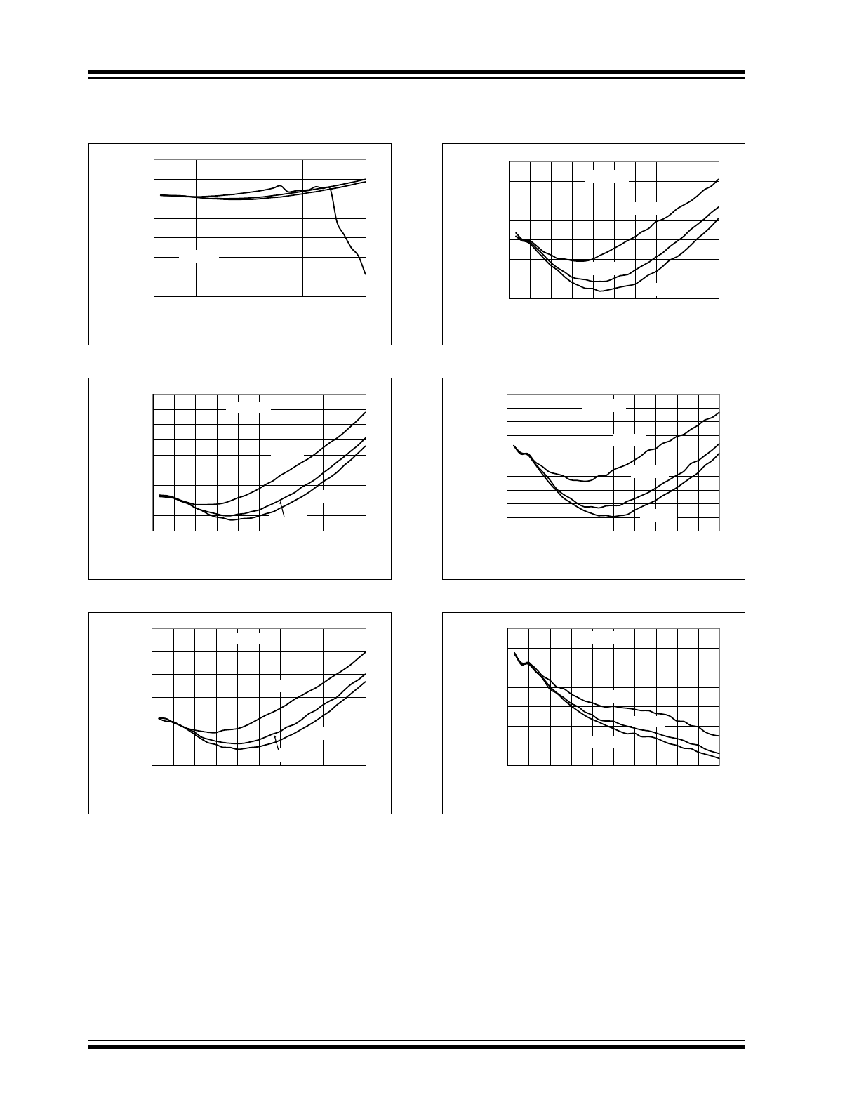
FIGURE 2-7:
5V V
OUT
vs. I
OUT.
FIGURE 2-8:
3.3V V
OUT
vs. I
OUT.
FIGURE 2-9:
2.5V V
OUT
vs. I
OUT.
FIGURE 2-10:
1.8V V
OUT
vs. I
OUT.
FIGURE 2-11:
1.5V V
OUT
vs. I
OUT.
FIGURE 2-12:
0.9V V
OUT
vs. I
OUT.
4.75
4.8
4.85
4.9
4.95
5
5.05
5.1
0
0.6
1.2
1.8
2.4
3
V
OUT
(V)
I
OUT
(A)
V
IN
= 6V
V
IN
= 12V
V
IN
= 18V
V
OUT
= 5V
3.295
3.3
3.305
3.31
3.315
3.32
3.325
3.33
3.335
3.34
0
0.6
1.2
1.8
2.4
3
V
OUT
(V)
I
OUT
(A)
V
IN
= 6V
V
IN
= 12V
V
IN
= 18V
V
OUT
= 3.3V
2.495
2.5
2.505
2.51
2.515
2.52
2.525
0
0.6
1.2
1.8
2.4
3
V
OUT
(V)
I
OUT
(A)
V
IN
= 6V
V
IN
= 12V
V
IN
= 18V
V
OUT
= 2.5V
1.798
1.8
1.802
1.804
1.806
1.808
1.81
1.812
0
0.6
1.2
1.8
2.4
3
V
OUT
(V)
I
OUT
(A)
V
IN
= 6V
V
IN
= 12V
V
IN
= 18V
V
OUT
=1.8V
1.498
1.499
1.5
1.501
1.502
1.503
1.504
1.505
1.506
1.507
1.508
0
0.6
1.2
1.8
2.4
3
V
OUT
(V)
I
OUT
(A)
V
IN
= 6V
V
IN
= 12V
V
IN
= 16V
V
OUT
=1.5V
0.897
0.898
0.899
0.9
0.901
0.902
0.903
0.904
0
0.6
1.2
1.8
2.4
3
V
OUT
(V)
I
OUT
(A)
V
IN
= 6V
V
IN
= 8V
V
IN
= 10V
V
OUT
=0.9V
2011-2016 Microchip Technology Inc.
DS20002284B-page 9
MCP16323
Note:
Unless otherwise indicated, V
IN
= 12V, EN = Floating (internally pulled up), C
IN
= 20 µF, C
OUT
= 2x22 µF,
L = 4.7 µH, I
LOAD
= 200 mA, T
A
= +25°C.
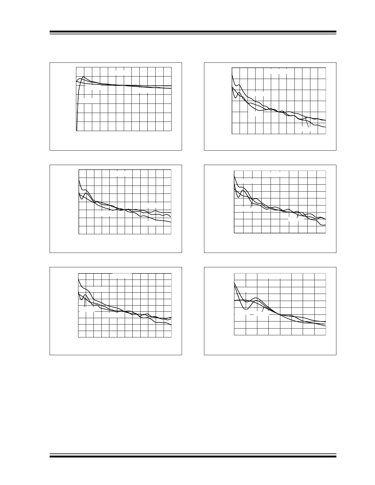
FIGURE 2-13:
5V V
OUT
vs. V
IN.
FIGURE 2-14:
3.3V V
OUT
vs. V
IN.
FIGURE 2-15:
2.5V V
OUT
vs. V
IN.
FIGURE 2-16:
1.8V V
OUT
vs. V
IN.
FIGURE 2-17:
1.5V V
OUT
vs. V
IN.
FIGURE 2-18:
0.9V V
OUT
vs. V
IN.
4.9
4.92
4.94
4.96
4.98
5
5.02
5.04
6
8
10
12
14
16
18
V
OUT
(V)
V
IN
(V)
I
OUT
= 1A
I
OUT
= 2A
V
OUT
= 5V
I
OUT
= 3A
3.294
3.296
3.298
3.3
3.302
3.304
3.306
3.308
3.31
6
8
10
12
14
16
18
V
OUT
(V)
V
IN
(V)
I
OUT
= 1A
I
OUT
= 2A
V
OUT
= 3.3V
I
OUT
= 3A
2.496
2.497
2.498
2.499
2.5
2.501
2.502
2.503
2.504
2.505
2.506
6
8
10
12
14
16
18
V
OUT
(V)
V
IN
(V)
I
OUT
= 1A
I
OUT
= 3A
V
OUT
= 2.5V
I
OUT
= 2A
1.798
1.799
1.8
1.801
1.802
1.803
1.804
6
8
10
12
14
16
18
V
OUT
(V)
V
IN
(V)
I
OUT
= 2A
I
OUT
= 1A
V
OUT
= 1.8V
I
OUT
= 3A
1.4985
1.499
1.4995
1.5
1.5005
1.501
1.5015
1.502
1.5025
1.503
6
8
10
12
14
16
V
IN
(V)
V
OUT
(V)
I
OUT
= 2A
I
OUT
= 1A
V
OUT
= 1.5V
I
OUT
= 3A
0.8994
0.8996
0.8998
0.9
0.9002
0.9004
0.9006
0.9008
0.901
0.9012
6
7
8
9
10
V
OUT
(V)
V
IN
(V)
I
OUT
= 2A
I
OUT
= 1A
V
OUT
= 0.9V
I
OUT
= 3A
MCP16323
DS20002284B-page 10
2011-2016 Microchip Technology Inc.
Note:
Unless otherwise indicated, V
IN
= 12V, EN = Floating (internally pulled up), C
IN
= 20 µF, C
OUT
= 2x22 µF,
L = 4.7 µH, I
LOAD
= 200 mA, T
A
= +25°C.
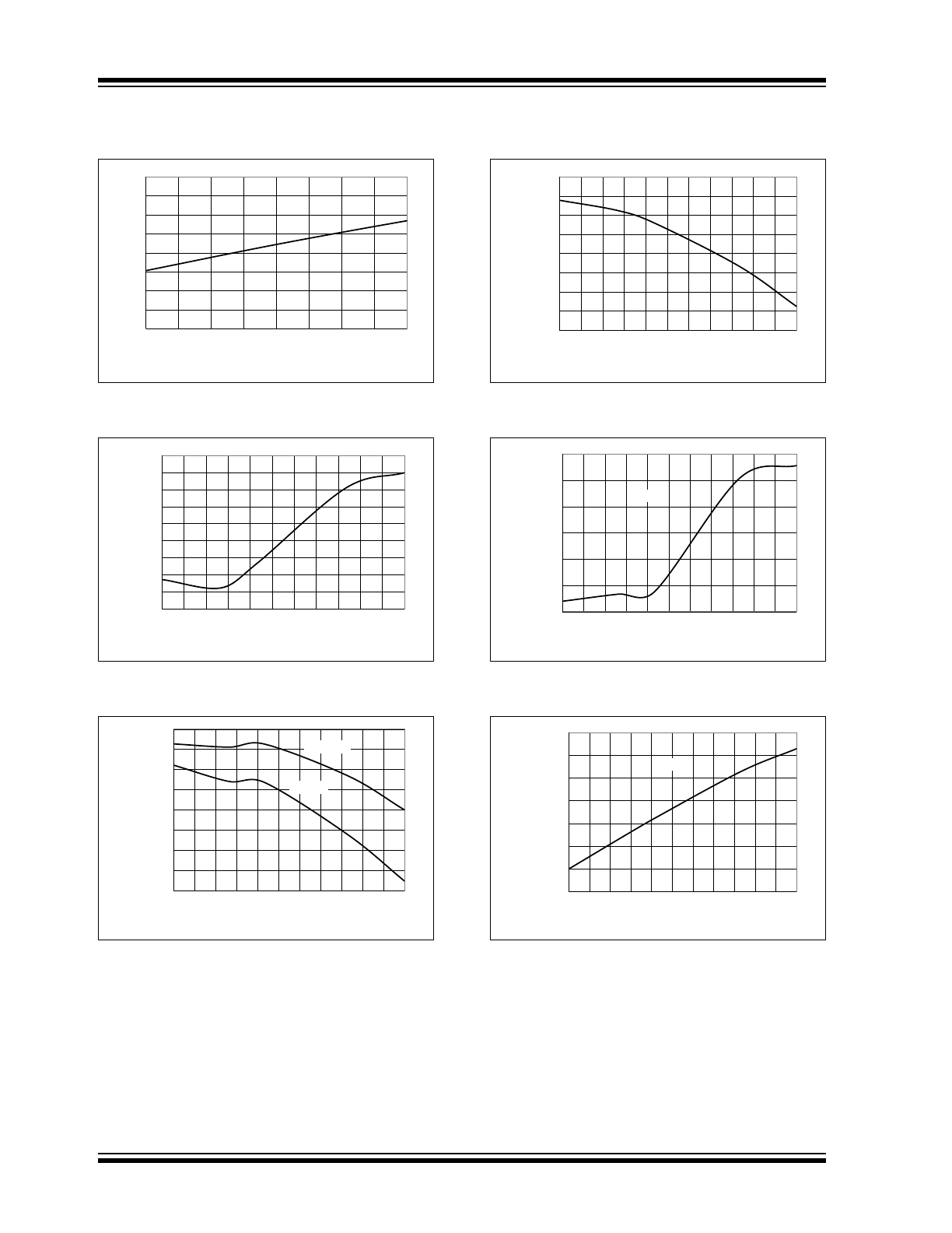
FIGURE 2-19:
Shutdown Current vs. Input
Voltage.
FIGURE 2-20:
Shutdown Current vs.
Temperature.
FIGURE 2-21:
Output Voltage vs.
Temperature.
FIGURE 2-22:
Oscillator Frequency vs.
Temperature (I
OUT
= 300 mA).
FIGURE 2-23:
Input Quiescent Current vs.
Temperature (No Load, Switching).
FIGURE 2-24:
Input Current vs.
Temperature (No Load, No Switching).
0
1
2
3
4
5
6
7
8
6
9
12
15
18
Shudow
n Current
(µA)
V
IN
(V)
4.45
4.50
4.55
4.60
4.65
4.70
4.75
4.80
4.85
4.90
-40
-10
20
50
80
110
Shutdow
n Current
(µA)
Ambient Temperature (°C)
3.284
3.286
3.288
3.290
3.292
3.294
3.296
3.298
3.300
-40
-10
20
50
80
110
V
OUT
(V)
Ambient Temperature (°C)
I
OUT
= 0.1A
I
OUT
= 1A
980
985
990
995
1000
1005
1010
1015
1020
-40
-10
20
50
80
110
Oscillator Frequency
(kHz)
Ambient Temperature (°C)
5.20
5.25
5.30
5.35
5.40
5.45
5.50
-40
-10
20
50
80
110
Sw
itching Quiscent
Current
(mA)
Ambent Temperature (°C)
I
OUT
= 0A
2.28
2.30
2.32
2.34
2.36
2.38
2.40
2.42
-40
-10
20
50
80
110
Non-Sw
itching Quiscent
Current
(mA)
Ambient Temperature (°C)
I
OUT
= 0A