
2017 Microchip Technology Inc.
DS20005881A-page 1
MIC5271
Features
• Stable with Ceramic or Tantalum Capacitors
• Standard Fixed Output Voltage Options: 3.0V and
5.0V
• Adjustable Output Voltage Option: (–1.2V to
–14V)
• Positive and Negative Enable Thresholds
• Low Dropout Voltage: –500 mV @ –100 mA
• Low Ground Current: –25 µA @ Load = –100 µA
• Tight Initial Accuracy: ±2%
• Tight Load and Line Regulation
• Thermal Shutdown and Current-Limit Protection
• IttyBitty 5-Pin SOT23 Packaging
• Zero-Current Off Mode
Applications
• GaAsFET Bias
• Portable Cameras and Video Recorders
• PDAs
• Battery-Powered Equipment
• Post-Regulation of DC/DC Converters
General Description
The MIC5271 is a µCap 100 mA negative regulator in
a SOT23-5 package. With better than 2% initial
accuracy, this regulator provides a very accurate
supply voltage for applications that require a negative
rail. The MIC5271 sinks 100 mA of output current at
very low dropout voltage (500 mV typical, 700 mV
maximum at 100 mA of output current).
The µCap regulator design is optimized to work with
low-value, low-cost ceramic capacitors. The output
typically requires only a 1 µF capacitance for stability.
Designed for applications where small packaging and
efficiency are critical, the MIC5271 combines LDO
design expertise with IttyBitty packaging to improve
performance and reduce power dissipation. Ground
current is optimized to help improve battery life in
portable applications. The MIC5271 also includes a
TTL-compatible enable pin, allowing the user to put the
part into a zero-current off mode, in which the ground
current is only ±1 µA, typical.
The MIC5271 is available in the 5-pin SOT23 package
for space saving applications and it is available with an
adjustable output.
Package Types
Please see pin descriptions in
Table 3-1
.
MIC5271YM5
5-Lead SOT23 (M5)
Adjustable Output Voltage
(Top View)
MIC5271-5.0YM5 *
5-Lead SOT23 (M5)
Fixed Output Voltage
(Top View)
* 5.0V pinout shown. 3.0V version is identical.
ADJ GND
–OUT
–IN
EN
3
1
5
2
4
L9AA
NC GND
–OUT
–IN
EN
3
1
5
2
4
L950
µCap Negative Low Dropout Regulator
MIC5271
DS20005881A-page 2
2017 Microchip Technology Inc.
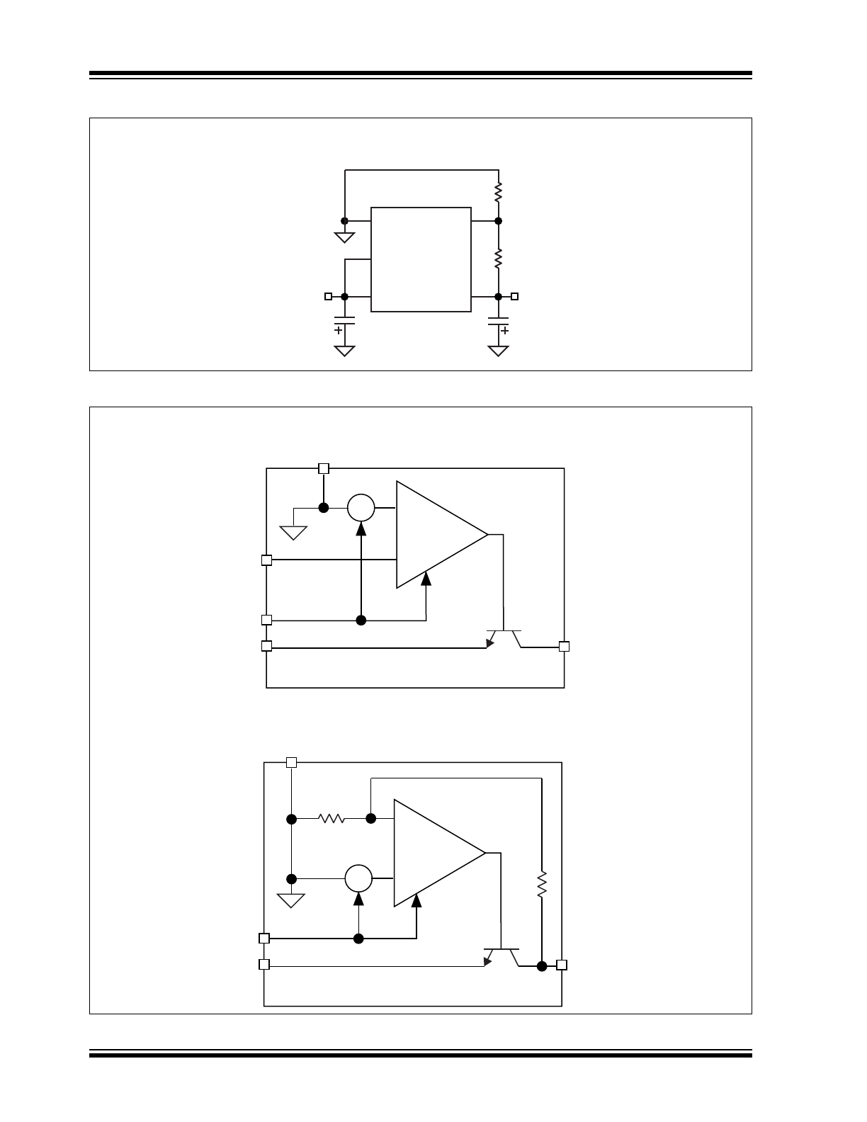
Typical Application Circuit
Functional Block Diagram
MIC5271
SOT23-5
V
IN
–6.0V
MIC5271YM5
1
2
3
4
5
1μF
10μF
R1
R2
V
OUT
–5.0V
GND
EN
–IN
ADJ
–OUT
–
+
GND
–OUT
–
+
ADJ
EN
–IN
MIC5271YM5
MIC5271YM5
(Adjustable Version)
–
+
GND
–
+
EN
MIC5271-x.xYM5
–OUT
–IN
MIC5271-x.xYM5
(Fixed Version)

2017 Microchip Technology Inc.
DS20005881A-page 3
MIC5271
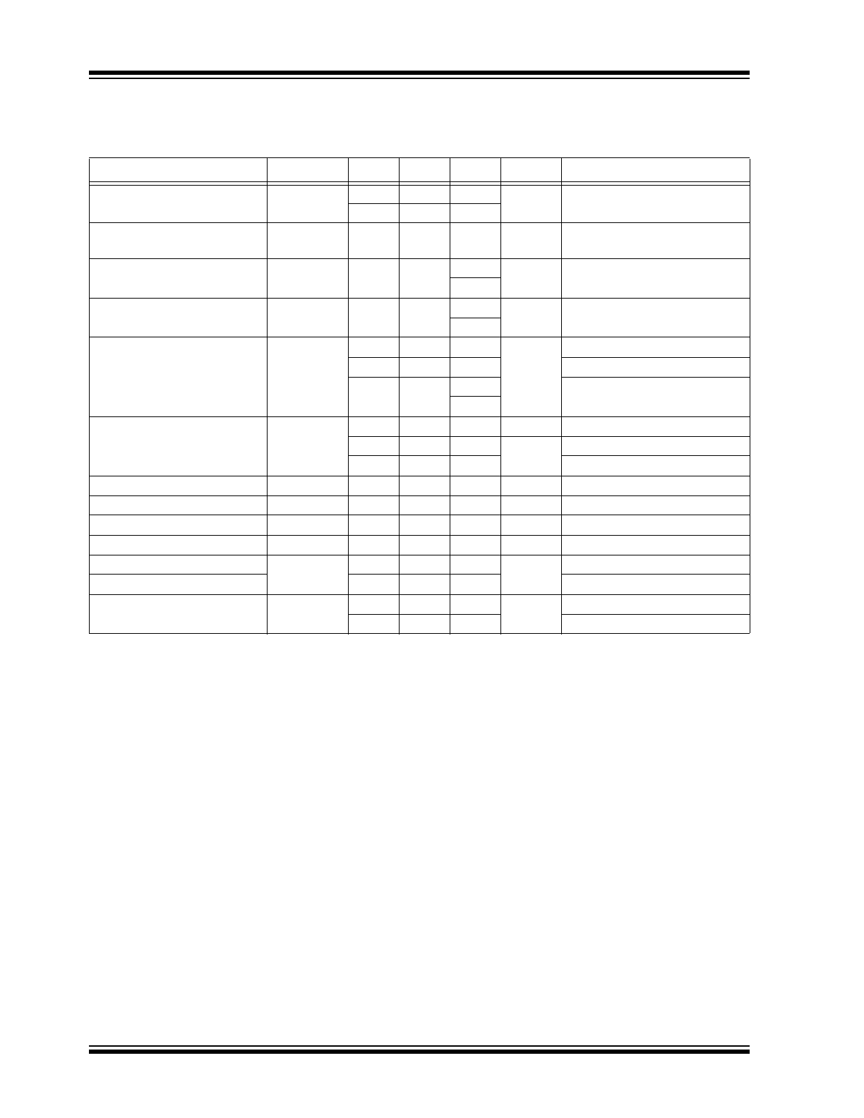
1.0
ELECTRICAL CHARACTERISTICS
Absolute Maximum Ratings †
Input Voltage (V–
IN
) ................................................................................................................................... –20V to +0.3V
Enable Voltage (V
EN
) .................................................................................................................................. –20V to +20V
Power Dissipation .................................................................................................................................. Internally Limited
ESD Rating .............................................................................................................................................................
Note 1
Operating Ratings ‡
Input Voltage (V–
IN
) ................................................................................................................................... –16V to –3.3V
Enable Voltage (V
EN
) .................................................................................................................................. –16V to +16V
†
Notice: Stresses above those listed under “Absolute Maximum Ratings” may cause permanent damage to the device.
This is a stress rating only and functional operation of the device at those or any other conditions above those indicated
in the operational sections of this specification is not intended. Exposure to maximum rating conditions for extended
periods may affect device reliability.
‡ Notice:
The device is not guaranteed to function outside its operating ratings.
Note 1:
Devices are ESD sensitive. Handling precautions recommended.
MIC5271
DS20005881A-page 4
2017 Microchip Technology Inc.
TABLE 1-1:
ELECTRICAL CHARACTERISTICS
Electrical Characteristics:
V–
IN
= V–
OUT
– 1.0V; C
OUT
= 4.7 µF, I
OUT
= 100 µA; T
J
= +25°C, bold values indicate
–40°C ≤ T
J
≤ +125°C; unless otherwise noted.
Note 1
Parameter
Symbol
Min.
Typ.
Max.
Units
Conditions
Output Voltage Accuracy
V–
OUT
–2
—
2
%
Variation from nominal V–
OUT
.
–3
—
3
Output Voltage Temperature
Coefficient
∆V–
OUT
/∆T
—
100
—
ppm/°C
Note 2
Line Regulation
∆V–
OUT
/
V–
OUT
—
0.04
0.15
%/V
V–
IN
= V–
OUT
– 1V to –16V
0.2
Load Regulation
∆V–
OUT
/
V–
OUT
—
0.4
1.8
%
I
OUT
= –100 µA to –100 mA,
Note 3
2.0
Dropout Voltage,
Note 4
V–
IN
–
V–
OUT
—
–55
—
mV
I
OUT
= –100 µA
—
–360
–500
I
OUT
= –50 mA
—
–500
–700
I
OUT
= –100 mA
–900
Ground Current,
Note 5
I
GND
—
–25
–100
µA
I
OUT
= –100 µA
—
–0.9
—
mA
I
OUT
= –50 mA
—
–2.0
–3.0
I
OUT
= –100 mA
Ground Current in Shutdown
I
GND_SD
–1.0
0.1
1.0
µA
V
EN
= ±0.6V
Ripple Rejection
PSRR
—
50
—
dB
f = 120 Hz
Current Limit
I
LIMIT
—
235
350
mA
V–
OUT
= 0V
Turn-On Time
t
ON
—
60
—
µs
Time to V
OUT
= 90% (nominal)
Input Low Voltage
V
EN
—
—
±0.6
V
Regulator OFF
Input High Voltage
±2.0
—
—
Regulator ON
Enable Input Current
I
EN
—
—
0.1
µA
V
EN
= ±0.6V and –2.0V
—
5.6
10.0
V
EN
= +2.0V
Note 1:
Specification for packaged product only
2:
Output voltage temperature coefficient is defined as the worst case voltage change divided by the total
temperature range.
3:
Regulation is measured at constant junction temperature using low duty cycle pulse testing. Parts are
tested for load regulation in the load range from 100 µA to 100 mA. Changes in output voltage due to heat-
ing effects are covered by the thermal regulation specification.
4:
Dropout voltage is defined as the input to output differential at which the output voltage drops 2% below its
nominal value measured at 1V differential.
5:
Ground pin current is the regulator quiescent current plus pass transistor base current. The total current
drawn from the supply is the sum of the load current plus the ground pin current.
2017 Microchip Technology Inc.
DS20005881A-page 5
MIC5271
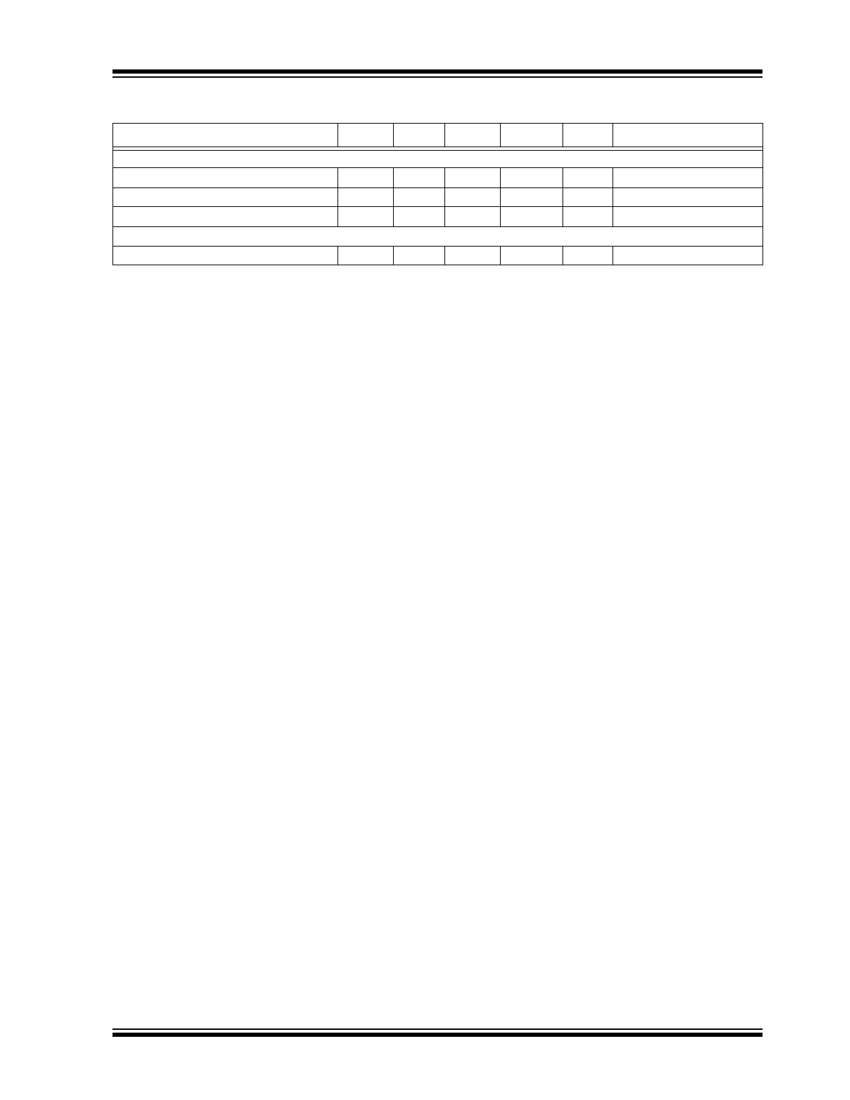
TEMPERATURE SPECIFICATIONS (
Note 1
)
Parameters
Sym.
Min.
Typ.
Max.
Units
Conditions
Temperature Ranges
Junction Temperature Range
T
J
–40
—
+125
°C
—
Storage Temperature Range
T
S
–65
—
+150
°C
—
Lead Temperature
—
—
—
+260
°C
Soldering, 10s
Package Thermal Resistances
Thermal Resistance SOT23-5
JA
—
235
—
°C/W
—
Note 1:
The maximum allowable power dissipation is a function of ambient temperature, the maximum allowable
junction temperature and the thermal resistance from junction to air (i.e., T
A
, T
J
,
JA
). Exceeding the
maximum allowable power dissipation will cause the device operating junction temperature to exceed the
maximum +125°C rating. Sustained junction temperatures above +125°C can impact the device reliability.
2:
The maximum allowable power dissipation is a function of the maximum junction temperature, T
J(MAX)
the
junction-to-ambient thermal resistance, θ
JA
, and the ambient temperature, T
A
. The maximum allowable
power dissipation at any ambient temperature is calculated using: P
D(MAX)
= (T
J(MAX)
– T
A
) ÷ θ
JA
, where
θ
JA
is 235°C/W. Exceeding the maximum allowable power dissipation will result in excessive die tempera-
ture, and the regulator will go into thermal shutdown. See the “Thermal Considerations” sub-section in the
Application Information for details.
MIC5271
DS20005881A-page 6
2017 Microchip Technology Inc.
2.0
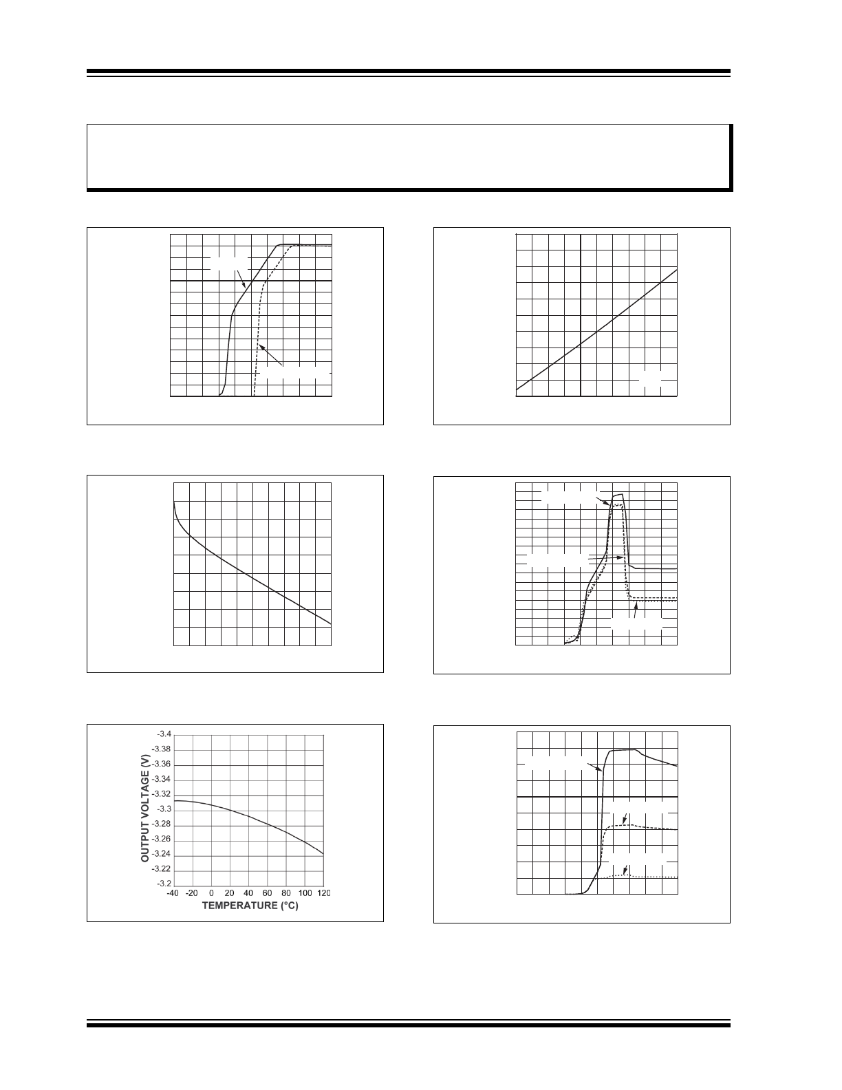
TYPICAL PERFORMANCE CURVES
FIGURE 2-1:
Dropout Characteristics.
FIGURE 2-2:
Output Voltage vs. Output
Current.
FIGURE 2-3:
Output Voltage vs.
Temperature.
FIGURE 2-4:
Ground Current vs. Output
Current.
FIGURE 2-5:
Ground Current vs. Input
Voltage.
FIGURE 2-6:
Ground Current vs. Input
Voltage.
Note:
The graphs and tables provided following this note are a statistical summary based on a limited number of
samples and are provided for informational purposes only. The performance characteristics listed herein
are not tested or guaranteed. In some graphs or tables, the data presented may be outside the specified
operating range (e.g., outside specified power supply range) and therefore outside the warranted range.
0
-0.5
-1
-1.5
-2
-2.5
-3
-3.5
OUTPUT VOLTAGE (V)
SUPPLY VOLTAGE (V)
0 LOAD
-100mA LOAD
0
-1
-2
-3
-4
-5
-3.26
-3.265
-3.27
-3.275
-3.28
-3.285
-3.29
-3.295
-3.3
-3.305
OUTPUT VOLTAGE (V)
OUTPUT CURRENT (mA)
0
-20
-40
-60
-80
-100
0
-0.5
-1
-1.5
-2
-2.5
0
GROUND CURRENT (mA)
OUTPUT CURRENT (mA)
5V
IN
-20
-40
-60
-80
-100
0
-10
-20
-30
-40
-50
-60
-70
-80
-90
GROUND CURRENT (μA)
SUPPLY VOLTAGE (V)
0μA LOAD
-100μA LOAD
-1mA LOAD
-1
-2
-3
-4
-5
0
0
-0.5
-1
-1.5
-2
-2.5
GROUND CURRENT (mA)
SUPPLY VOLTAGE (V)
-100mA LOAD
-50mA LOAD
-10mA LOAD
0
-1
-2
-3
-4
-5
2017 Microchip Technology Inc.
DS20005881A-page 7
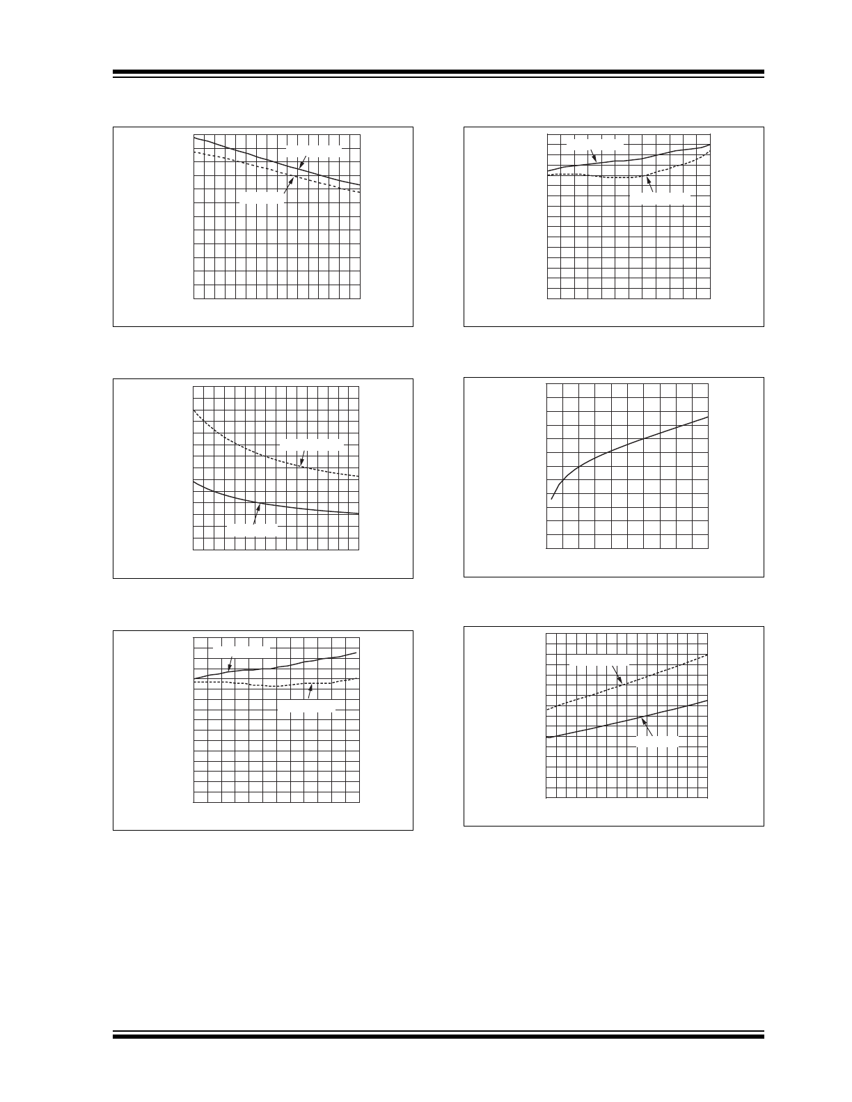
MIC5271
FIGURE 2-7:
Ground Current vs.
Temperature.
FIGURE 2-8:
Ground Current vs.
Temperature.
FIGURE 2-9:
Positive Enable Threshold
vs. Supply Voltage.
FIGURE 2-10:
Negative Enable Threshold
vs. Supply Voltage.
FIGURE 2-11:
Dropout Voltage vs. Output
Current.
FIGURE 2-12:
Dropout Voltage vs.
Temperature.
0
-5
-10
-15
-20
-25
-30
GROUND CURRENT (
μA)
TEMPERATURE (°C)
0A LOAD
-1mA LOAD
-40 -20
0
20
40
60
80 100 120
0
-0.5
-1
-1.5
-2
-2.5
-3
-3.5
GROUND CURRENT (
μA)
TEMPERATURE (°C)
-50mA LOAD
-100mA LOAD
-40 -20
0
20
40
60
80 100 120
0
0.2
0.4
0.6
0.8
1
1.2
1.4
1.6
ENABLE THRESHOLD (V)
SUPPLY VOLTAGE (V)
ENABLE OFF
ENABLE ON
-4
-7
-10
-13
-16
0
-0.2
-0.4
-0.6
-0.8
-1
-1.2
-1.4
-1.6
ENABLE THRESHOLD (V)
SUPPLY VOLTAGE (V)
ENABLE OFF
ENABLE ON
-4
-7
-10
-13
-16
0
-100
-200
-300
-400
-500
-600
0
DROPOUT VOLTAGE (mV)
OUTPUT CURRENT (mA)
-20
-40
-60
-80
-100
0
-50
-100
-150
-200
-250
-300
-350
-400
DROPOUT VOLTAGE (mV)
TEMPERATURE (°C)
0A LOAD
-10mA LOAD
-40 -20
0
20
40
60
80 100 120
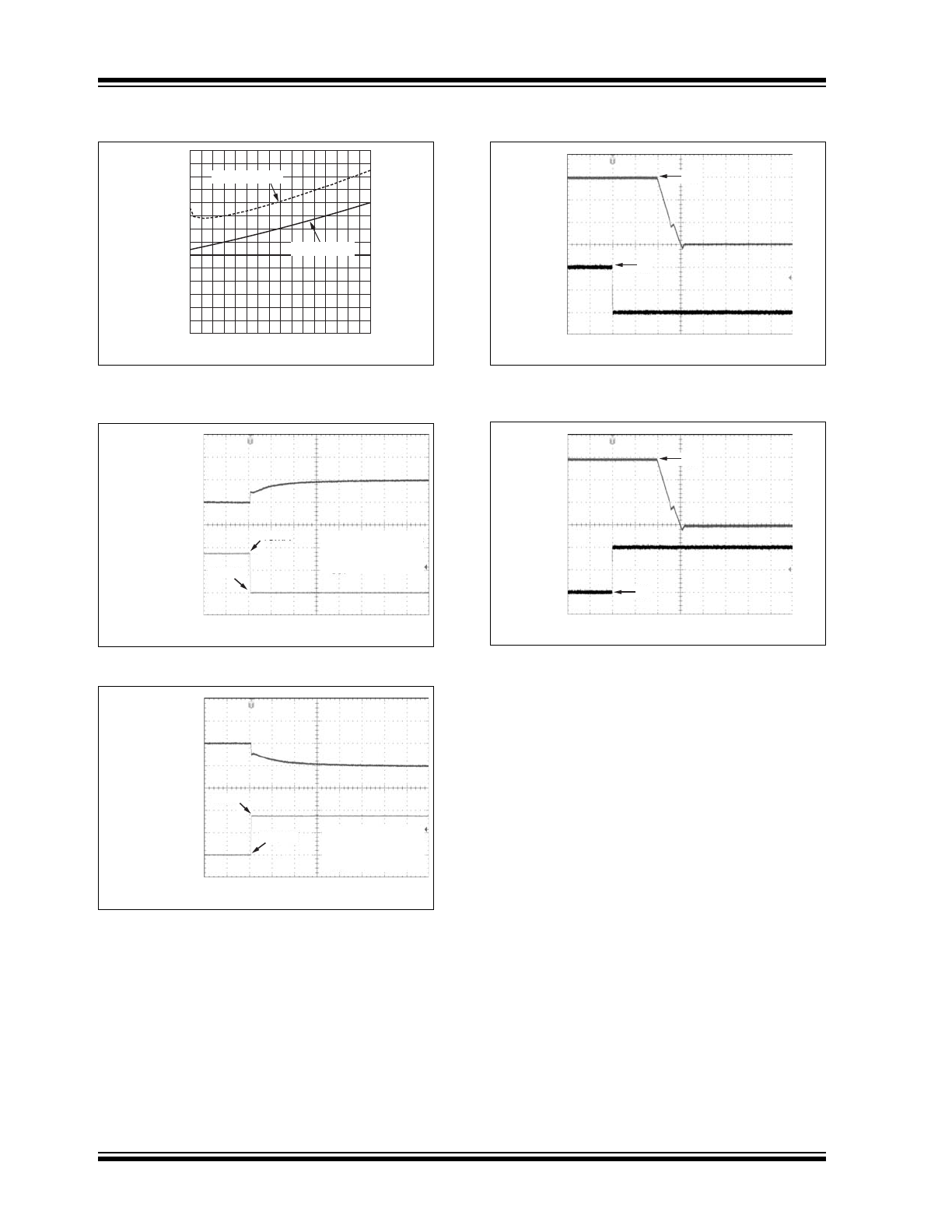
MIC5271
DS20005881A-page 8
2017 Microchip Technology Inc.
FIGURE 2-13:
Dropout Voltage vs.
Temperature
.
FIGURE 2-14:
Load Transient
.
FIGURE 2-15:
Load Transient.
FIGURE 2-16:
Negative Enable Transient.
FIGURE 2-17:
Positive Enable Transient.
0
-100
-200
-300
-400
-500
-600
-700
DROPOUT VOLTAGE (mV)
TEMPERATURE (°C)
-50mA LOAD
-100mA LOAD
-40 -20
0
20
40
60
80 100 120
Time (2ms/div)
OUTPUT CURRENT
(50mA/div)
V
OUT
(AC-COUPLED)
(10mV/div)
C
OUT
= 1μF CERAMIC
V
IN
= –5V
V
OUT
= –3V
–10mA
-100mA
Time (2ms/div)
OUTPUT CURRENT
(50mA/div)
V
OUT
(AC-COUPLED)
(10mV/div)
C
OUT
= 1μF CERAMIC
V
IN
= –5V
V
OUT
= –3V
–10mA
–100mA
Time (20μs/div)
ENABLE
(1V/div)
V
OUT
(1V/div)
0V
0V
Time (20μs/div)
ENABLE
(1V/div)
V
OUT
(1V/div)
0V
0V
2017 Microchip Technology Inc.
DS20005881A-page 9
MIC5271
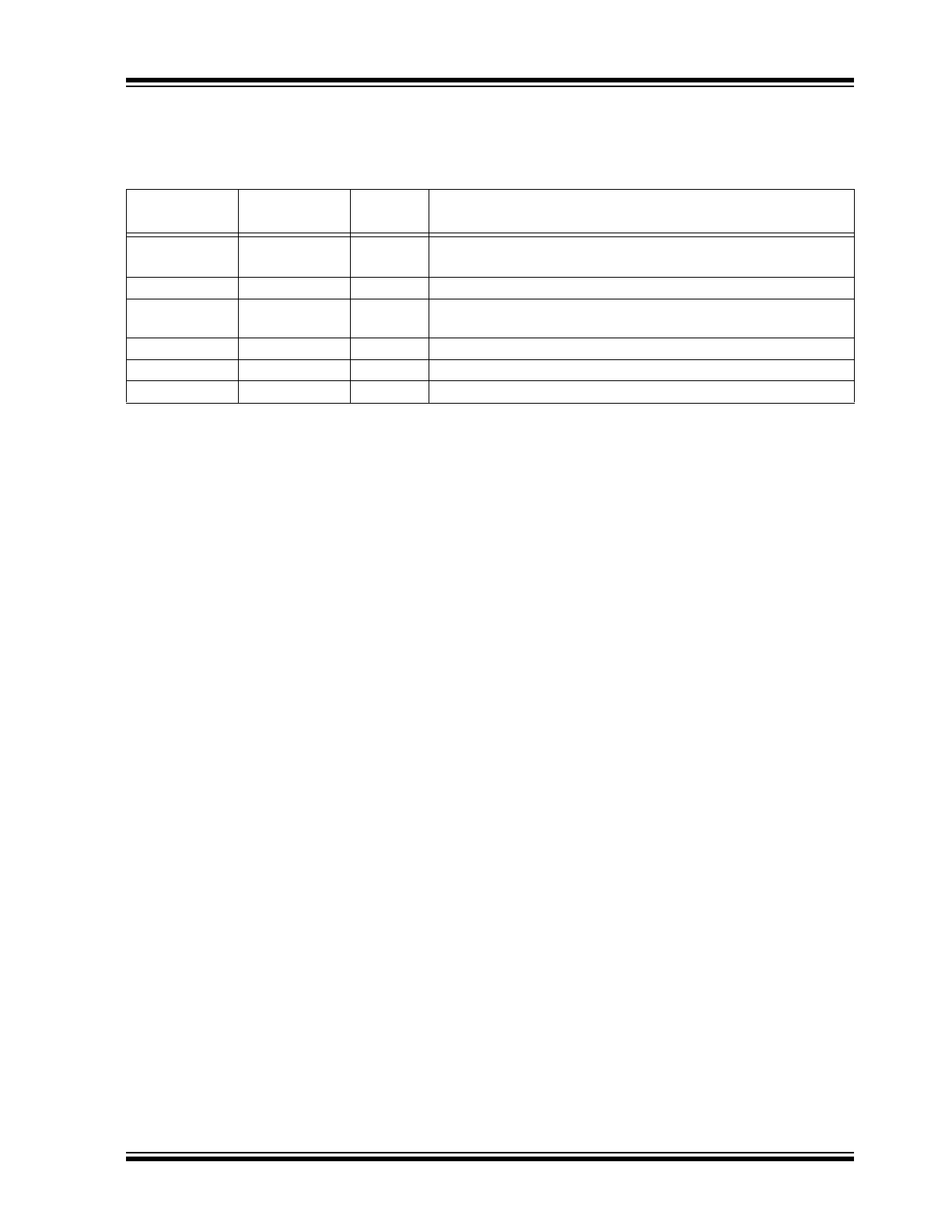
3.0
PIN DESCRIPTIONS
The descriptions of the pins are listed in
Table 3-1
.
TABLE 3-1:
PIN FUNCTION TABLE
Pin Number
Adjustable
Pin Number
Fixed
Pin Name
Description
1
1
EN
Enable Input. TTL logic-compatible enable input. Logic HIGH = ON,
Logic LOW or open = OFF.
2
2
GND
Ground.
3
—
ADJ
Adjustable (Input): Adjustable feedback output connects to resistor
voltage divider.
—
3
NC
No Connect. Leave unconnected.
4
4
–OUT
Negative Regulator Output.
5
5
–IN
Negative Supply Input.
MIC5271
DS20005881A-page 10
2017 Microchip Technology Inc.
4.0
APPLICATION INFORMATION
The MIC5271 is a general-purpose negative voltage
regulator that can be used in a system that requires a
clean negative voltage. This includes the post
regulation of DC/DC converters (transformer or charge
pump based voltage converters). These negative
voltages typically require a negative low dropout
voltage regulator to provide a clean output from noisy
input power.
4.1
Input Capacitor
A 1 µF input capacitor should be placed from –IN to
GND if there is more than two inches of wire or trace
between the input and the AC filter capacitor or if a
battery is used as the input.
4.2
Output Capacitor
The MIC5271 requires an output capacitor for stable
operation. A minimum of 1 µF of output capacitance is
required. The output capacitor can be increased
without limitation to improve transient response. The
output does not require ESR to maintain stability;
therefore a ceramic capacitor can be used. High-ESR
capacitors may cause instability. Capacitors with an
ESR of 3Ω or greater at 100 kHz can cause a
high-frequency oscillation.
Low-ESR tantalums are recommended due to the tight
capacitance tolerance over temperature. The Z5U
dielectric can change capacitance value by as much
50% over temperature, and the Y5V dielectric can
change capacitance value by as much as 60% over
temperature. To use a ceramic chip capacitor with the
Y5V dielectric, the value must be much higher than a
tantalum to ensure the same minimum capacitor value
over temperature.
4.3
No-Load Stability
The MIC5271 does not require a load for stability.
4.4
Enable Input
The MIC5271 comes with an enable pin that allows the
regulator to be disabled. Forcing the enable pin higher
than the negative threshold and lower than the positive
threshold disables the regulator and sends it into a
“zero” off-mode current state. In this state, current
consumed by the regulator goes nearly to zero,
typically drawing only ±1 µA. The MIC5271 will be in
the “on” mode when the voltage applied to the enable
pin is either greater than the positive threshold or less
than the negative threshold.
FIGURE 4-1:
Positive and Negative
Enable Voltage vs. Supply Voltage.
4.5
Thermal Considerations
Absolute values will be used for thermal calculations to
clarify the meaning of power dissipation and voltage
drops across the part.
Proper thermal design for the MIC5271-5.0YM5 can be
accomplished with some basic design criteria and
some simple equations. The following information must
be known to implement your regulator design:
• V
IN
= Input voltage
• V
OUT
= Output voltage
• I
OUT
= Output current
• T
A
= Ambient operating temperature
• I
GND
= Ground current
Maximum power dissipation can be determined by
knowing the ambient temperature (T
A
), the maximum
junction temperature (+125°C), and the thermal
resistance (junction-to-ambient). The thermal
resistance for this part, assuming a minimum footprint
board layout, is +235°C/W. The maximum power
dissipation at an ambient temperature of +25°C can be
determined with
Equation 4-1
and
Equation 4-2
:
ENABLE VOL
TAGE (V)
5
4
3
2
1
0
–1
–2
–3
–4
–5
–7
–15
–3
–13
–11
–9
ENABLE INPUT
REGULATOR ON
REGULATOR OFF
REGULATOR ON
SUPPLY VOLTAGE (V)
–5