
2007-2011 Microchip Technology Inc.
DS22050B-page 1
MCP2140A
Features
• Implements the IrDA
®
Protocols, including:
- IrLAP
- IrLMP
- IAS
- Tiny TP
- IrCOMM (9-wire “cooked” service class)
• Provides IrDA standard physical signal layer
support including:
- Bidirectional communication
- CRC implementation
- Fixed Data communication rate of 9600 baud
• Includes UART-to-IrDA standard encoder/decoder
functionality:
Easily interfaces with industry standard
UARTs and infrared transceivers
• Easily communicates with 16-bit PIC
Microcontroller IrDA Standard Stack Library
• UART interface for connecting to Data
Communications Equipment (DCE) or Data
Terminal Equipment (DTE) systems
• Transmit/Receive formats (bit width) supported:
- 1.63 µs (Transmit & Receive)
- 3/16 bit time (Receive Only)
• Hardware UART Support:
- 9.6 kbaud baud rate
- 60 Byte Data Buffer Size (64 Byte Packet)
• Infrared Supported:
- 9.6 kbaud baud rate
- 64 Byte Packet Size (60 Data Bytes)
• Operates as Secondary Device
• Wide Operating Voltage: 2.0V to 5.5V
• Automatic Low Power mode:
< 23 µA (maximum) @ 2.0V, when
no IR activity present (PHACT = L)
• Footprint Compatibility with MCP2140
CMOS Technology
• Low power, high-speed CMOS technology
• Low voltage operation
• Industrial temperature range
• Low power consumption:
< 407 µA (maximum) @ 2.0V, 3.6864 MHz
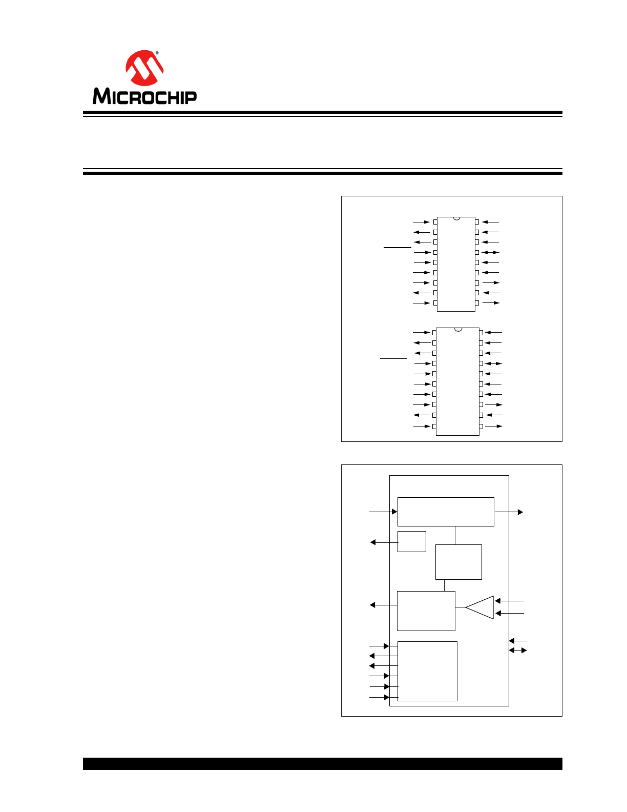
Package Types
Block Diagram
2
3
4
5
6
7
8
9
10
1
2
3
4
5
6
7
8
9
1
19
18
16
15
14
13
12
11
17
18
17
15
14
13
12
11
10
16
20
OSC2/CLKI
OSC1
V
SS
V
SS
V
DD
V
DD
RXPD
CD
CTS
RTS
TX
RX
RI
DSR
DTR
TXIR
PHACT
RESET
NC
RXPDREF
V
SS
TX
RX
RI
TXIR
PHACT
RESET
NC
RXPDREF
OSC2/CLKI
OSC1
V
DD
RXPD
CD
CTS
RTS
DSR
DTR
MCP
214
0A
MCP
214
0A
PDIP, SOIC
SSOP
Encode and
Protocol
TX
TXIR
RX
RXPD
MCP2140A
Baud
RTS
Generator
CD
CTS
DSR
DTR
RI
OSC1
OSC2/
Protocol Handler
and Decode
RXPDREF
Handler
+
-
PHACT
Logic
Rate
UART
Control
CLKI
IrDA
®
Standard Protocol Stack Controller
With Fixed 9600 Baud Communication Rate

MCP2140A
DS22050B-page 2
2007-2011 Microchip Technology Inc.
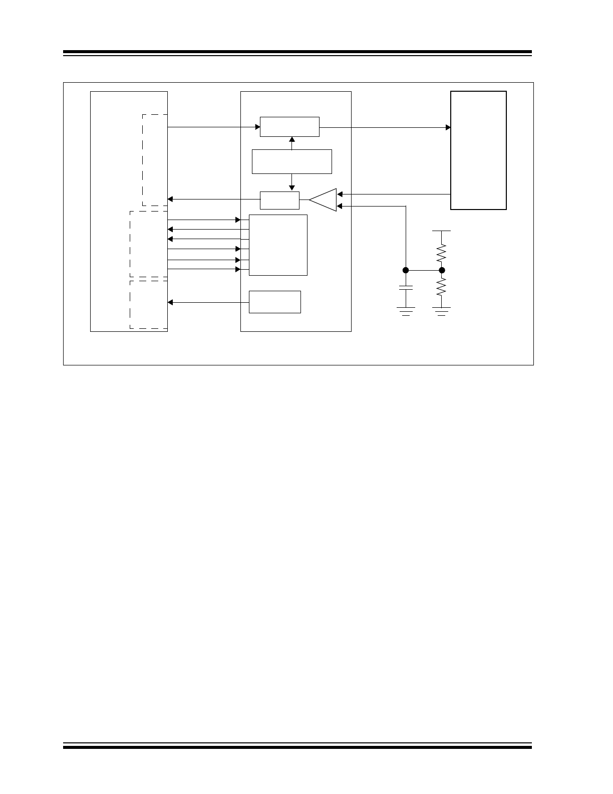
MCP2140A System Block Diagram
Encode
Decode
TX
TXIR
RX
I/O
MCP2140A
PIC
®
SO
SI
UAR
T
Baud Rate
Generator
UART
Control
Logic
RXPD
RXPDREF
+
-
RTS
CTS
DSR
DTR
CD
RI
PHACT
UAR
T
F
lo
w
I/O
I/O
I/O
I/O
I/O
I/O
Cont
rol (1)
M
C
P
2
14
0A
S
tatus
(1
)
Note 1: Not all microcontroller I/O pins are required to be connected to the MCP2140A.
Microcontroller
Optical
TXD
RXD
Transceiver
R1 (100 k
)
R2 (100 k
)
0.1 µF

2007-2011 Microchip Technology Inc.
DS22050B-page 3
MCP2140A
1.0
DEVICE OVERVIEW
The MCP2140A is a cost-effective, low pin count (18-
pin), easy-to-use device for implementing IrDA stan-
dard wireless connectivity. The MCP2140A provides
support for the IrDA standard protocol “stack”, bit
encoding/decoding and low cost, discrete IR receiver
circuitry. The MCP2140A is footprint compatible with
the MCP2140. For migration assistance, please refer to
Section 2.14 “Migrating from the MCP2140 to the
MCP2140A”.
The serial and IR interface baud rates are fixed at
9600 baud. The serial interface and IR interface baud
rates are dependent on the device frequency, but IrDA
standard operation requires a device frequency of
3.6864 MHz.
The MCP2140A will specify the IR baud rate to the pri-
mary device during the Discover phase.
The MCP2140A can operate in Data Communication
Equipment (DCE) and Data Terminal Equipment (DTE)
applications, and resides between a UART and an
infrared optical transceiver.
The MCP2140A encodes an asynchronous serial data
stream, converting each data bit to the corresponding
infrared (IR) formatted pulse. IR pulses received are
decoded and then handled by the protocol handler
state machine. The protocol handler sends the appro-
priate data bytes to the host controller in UART
formatted serial data.
The MCP2140A supports “point-to-point” applications,
that is, one primary device and one secondary device.
The MCP2140A operates as a secondary device and
does not support “multi-point” applications.
Sending data using IR light requires some hardware
and the use of specialized communication protocols.
These protocol and hardware requirements are
described, in detail, by the IrDA standard specifica-
tions. The encoding/decoding functionality of the
MCP2140A is designed to be compatible with the phys-
ical layer component of the IrDA standard. This part of
the standard is often referred to as “IrPHY”.
Some of the devices that are compatible with the
MCP2140A include:
• PCs with IR ports
• PDAs
• 16-bit PIC Microcontroller IrDA Standard Stack
Library
More information about IrDA standards, specifications
and protocols can be found on the IrDA web site at
www.IrDA.org.
1.1
Applications
The MCP2140A infrared communications controller,
supporting the IrDA standard, provides embedded sys-
tem designers with the easiest way to implement IrDA
standard wireless connectivity.
Figure 1-1
shows a typ-
ical application block diagram, while
Table 1-2
shows
the pin definitions.
TABLE 1-1:
OVERVIEW OF FEATURES
Infrared communication is a wireless, two-way data
connection using infrared light generated by low-cost
transceiver signaling technology. This provides reliable
communication between two devices.
Infrared technology offers:
• Universal standard for connecting portable
computing devices
• Easy, effortless implementation
• Economical alternative to other connectivity
solutions
• Reliable, high-speed connections
• Safe to use in any environment (can even be
used during air travel)
• No emissions testing needed (FCC, Part 15)
• Eliminates the hassle of cables
• Allows PCs and other electronic devices (such as
PDAs, cell phones, etc.) to communicate with
each other
• Enhances mobility by allowing users to easily
connect
The MCP2140A allows the easy addition of IrDA stan-
dard wireless connectivity to any embedded applica-
tion that uses serial data.
Figure 1-1
shows typical
implementation of the MCP2140A in an embedded
system.
The IrDA protocol for printer support is not included in
the IrCOMM 9-wire “cooked” service class.
Features
MCP2140A
Serial Communications
UART, IR
Baud Rate Selection
Fixed
Low Power Mode
Yes - Automatic
Resets (and Delays)
RESET, POR
(PWRT and OST)
Packages
18-pin DIP, SOIC,
20-pin SSOP
MCP2140A
DS22050B-page 4
2007-2011 Microchip Technology Inc.
FIGURE 1-1:
SYSTEM BLOCK DIAGRAM
Encode
Decode
TX
TXIR
RX
I/O
MCP2140A
PIC®
SO
SI
UAR
T
Baud Rate
Generator
UART
Control
Logic
RXPD
RXPDREF
+
-
RTS
CTS
DSR
DTR
CD
RI
PHACT
UAR
T
F
lo
w
I/O
I/O
I/O
I/O
I/O
I/O
Contro
l (1
)
M
C
P21
40A
S
ta
tus
(1)
Note 1: Not all microcontroller I/O pins are required to be connected to the MCP2140A.
Microcontroller
Optical
TXD
RXD
Transceiver
R1 (100 k
)
R2 (100 k
)
0.1 µF
2007-2011 Microchip Technology Inc.
DS22050B-page 5
MCP2140A
TABLE 1-2:
MCP2140A PIN DESCRIPTION NORMAL OPERATION (DCE)
Pin Name
Pin Number
Pin
Type
Buffer
Type
PDIP
SOIC SSOP
Description
RXPDREF
1
1
1
I
A
IR Receive Photo Detect Diode Reference Voltage. This
voltage will typically be in the range of V
DD
/2.
TXIR
2
2
2
O
—
Asynchronous transmit to IrDA transceiver.
PHACT
3
3
3
OC
—
Protocol Handler Active. Indicates the state of the
MCP2140A Protocol Handler. This output is an open
collector, so an external pull-up resistor may be required.
1 = Protocol Handler is in the Discovery or NRM state
0 = Protocol Handler is in NDM state or the MCP2140A is in
Low Power mode
RESET
4
4
4
I
ST
Resets the Device
V
SS
5
5
5, 6
—
P
Ground reference for logic and I/O pins
NC
6
6
7
I
—
No connect
TX
7
7
8
I
TTL
Asynchronous receive; from host controller UART
RX
8
8
9
O
—
Asynchronous transmit; to host controller UART
RI
9
9
10
I
TTL
Ring Indicator. The state of this bit is communicated to the
IrDA primary device.
1 = No Ring Indicate Present
0 = Ring Indicate Present
DSR
10
10
11
O
—
Data Set Ready. Indicates that the MCP2140A has estab-
lished a valid IrDA link with a primary device
(1)
. This signal is
locally emulated and not related to the DTR bit of the IrDA
primary device.
1 = An IR link has not been established
(No IR Link)
0 = An IR link has been established (IR Link)
DTR
11
11
12
I
TTL
Data Terminal Ready. Indicates that the Embedded device
connected to the MCP2140A is ready for IR data. The state
of this bit is communicated to the IrDA primary device via
the IrDA DSR bit carried by IrCOMM.
1 = Embedded device not ready
0 = Embedded device ready
CTS
12
12
13
O
—
Clear to Send. Indicates that the MCP2140A is ready to
receive data from the host controller. This signal is locally
emulated and not related to the CTS/RTS bit of the IrDA pri-
mary device.
1 = Host controller should not send data
0 = Host controller may send data
Legend:
TTL = TTL compatible input
ST = Schmitt Trigger input with CMOS levels
A = Analog
P = Power
CMOS = CMOS compatible input
OC = Open collector output
I = Input
O = Output
Note 1: The state of the DSR output pin does not reflect the state of the DTR bit of the IrDA primary device.
MCP2140A
DS22050B-page 6
2007-2011 Microchip Technology Inc.
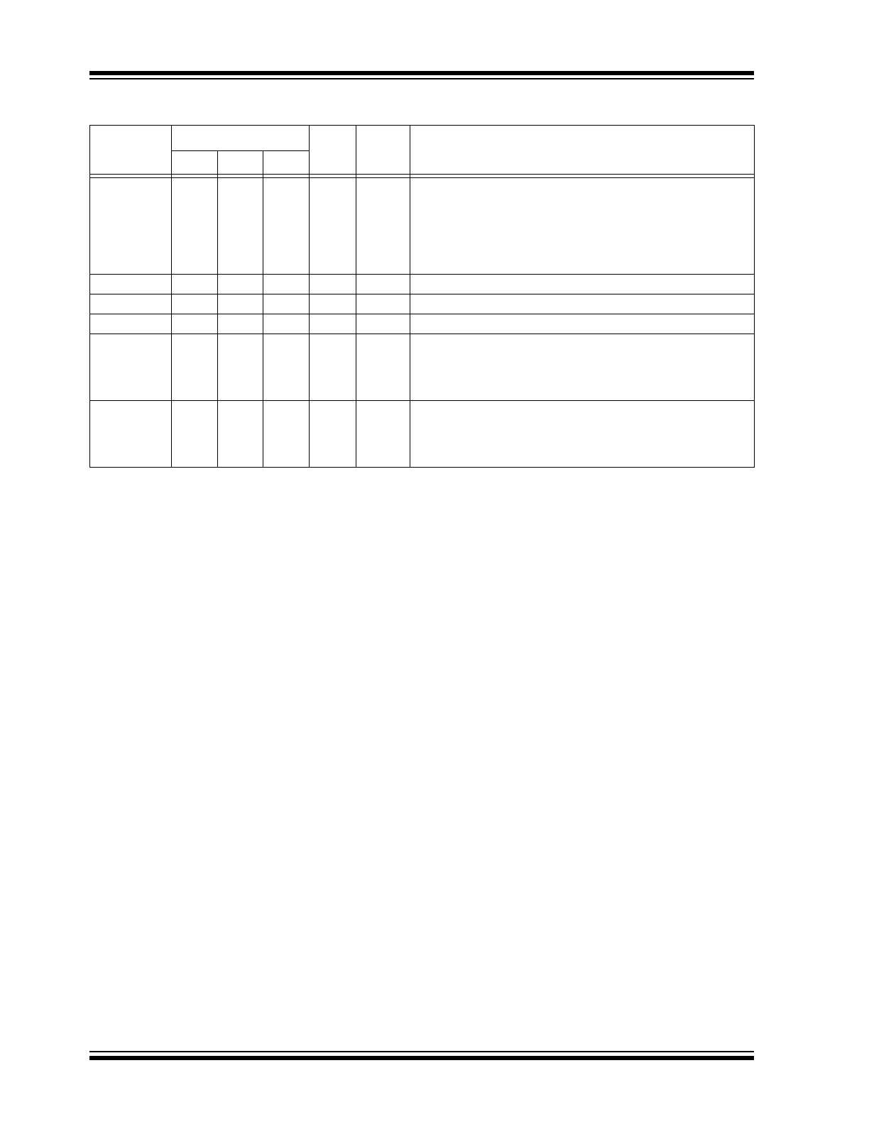
RTS
13
13
14
I
TTL
Request to Send. Indicates that a host controller is ready to
receive data from the MCP2140A. This signal is locally emu-
lated and not related to the CTS/RTS bit of the IrDA primary
device.
1 = Host controller not ready to receive data
0 = Host controller ready to receive data
V
DD
14
14
15, 16
—
P
Positive supply for logic and I/O pins.
OSC2/CLKI
15
15
17
I/O
—
Oscillator crystal output/external clock source input.
OSC1
16
16
18
I
CMOS Oscillator crystal input.
CD
17
17
19
I
ST
Carrier Detect. The state of this bit is communicated to the
IrDA primary device via the IrDA CD bit.
1 = No carrier present
0 = Carrier present
RXPD
18
18
20
I
A
IR RX Photo Detect Diode input. This input signal is required
to be a pulse to indicate an IR bit. When the amplitude of the
signal crosses the amplitude threshold set by the RXPDREF
pin, the IR bit is detected.
TABLE 1-2:
MCP2140A PIN DESCRIPTION NORMAL OPERATION (DCE) (CONTINUED)
Pin Name
Pin Number
Pin
Type
Buffer
Type
PDIP
SOIC SSOP
Description
Legend:
TTL = TTL compatible input
ST = Schmitt Trigger input with CMOS levels
A = Analog
P = Power
CMOS = CMOS compatible input
OC = Open collector output
I = Input
O = Output
Note 1: The state of the DSR output pin does not reflect the state of the DTR bit of the IrDA primary device.
2007-2011 Microchip Technology Inc.
DS22050B-page 7
MCP2140A
2.0
DEVICE OPERATION
The MCP2140A serial interface and IR baud rates are
fixed at 9600 baud, given a 3.6864 MHz device clock.
2.1
Power-Up
Any time the device is powered up (
Parameter D003
),
the Power-Up Timer delay (
Parameter 33
) occurs, fol-
lowed by an Oscillator Start-up Timer (OST) delay
(
Parameter 32
). Once these delays are complete, com-
munication with the device may be initiated. This com-
munication is from both the infrared transceiver’s side
and the controller’s UART interface.
2.1.1
POWER-ON AND BROWN-OUT
CONDITIONS
When any state machine is operated outside of its’
specified operating conditions, undesired operation
may occur. Application validation should be done to
determine when the system exits from either a Power-
On or a Brown-Out conditions if the MCP2140A
requires the use of an external voltage supervisory
circuit to ensure proper system operation.
2.2
Device Reset
The MCP2140A is forced into the Reset state when the
RESET pin is in the low state. Once the RESET pin is
brought to a high state, the device Reset sequence
occurs. Once the sequence completes, functional
operation begins.
2.3
Device Clocks
The MCP2140A requires a clock source to operate.
This clock source is used to establish the device timing,
including the device “Bit Clock”.
2.3.1
CLOCK SOURCE
The clock source can be supplied by one of the
following:
• Crystal
• Resonator
• External clock
The frequency of this clock source must be
3.6864 MHz (electrical specification
Parameter 1A
) for
device communication at 9600 baud.
2.3.1.1
Crystal Oscillator / Ceramic
Resonators
A crystal or ceramic resonator can be connected to the
OSC1 and OSC2 pins to establish oscillation (refer to
Figure 2-1
). The MCP2140A oscillator design requires
the use of a parallel-cut crystal. Use of a series cut
crystals may give a frequency outside of the crystal
manufacturers specifications.
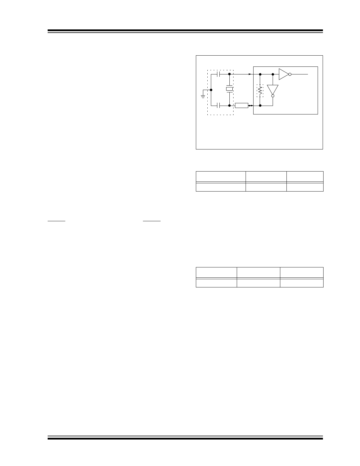
FIGURE 2-1:
CRYSTAL OPERATION
(CERAMIC RESONATOR)
TABLE 2-1:
CAPACITOR SELECTION FOR
CERAMIC RESONATORS
TABLE 2-2:
CAPACITOR SELECTION FOR
CRYSTAL OSCILLATOR
Freq
OSC1 (C1)
OSC2 (C2)
3.6864 MHz
10 - 22 pF
10 - 22 pF
Note:
Higher capacitance increases the stability
of the oscillator, but also increases the
start-up time. These values are for design
guidance only. Since each resonator has
its own characteristics, the user should
consult the resonator manufacturer for
appropriate values of external
components.
Freq
OSC1 (C1)
OSC2 (C2)
3.6864 MHz
15 - 30 pF
15 - 30 pF
Note:
Higher capacitance increases the stability
of the oscillator but also increases the
start-up time. These values are for design
guidance only. R
S
may be required to
avoid overdriving crystals with low drive
level specification. Since each crystal has
its own characteristics, the user should
consult the crystal manufacturer for
appropriate values of external
components.
See
Table 2-1
and
Table 2-2
for recommended
values of C1 and C2.
Note:
A series resistor may be required for
AT strip cut crystals.
C1
C2
XTAL
OSC2
RS
OSC1
RF
To internal
MCP2140A
(Note)
logic
Ceramic
Resonator
MCP2140A
DS22050B-page 8
2007-2011 Microchip Technology Inc.
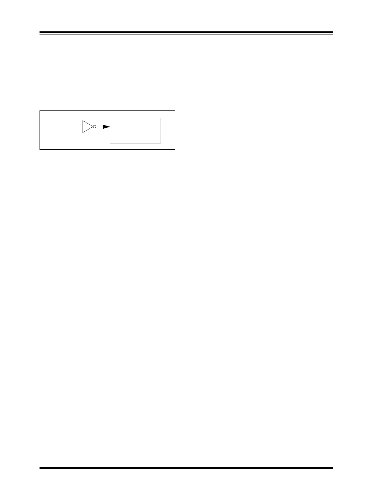
2.3.1.2
External Clock
For applications where a clock is already available
elsewhere, users may directly drive the MCP2140A
provided that this external clock source meets the AC/
DC timing requirements listed in
Section 4.3 “Timing
Diagrams and Specifications”
.
Figure 2-2
shows
how an external clock circuit should be configured.
FIGURE 2-2:
EXTERNAL CLOCK
2.3.2
BIT CLOCK
The device crystal is used to derive the communication
bit clock (BITCLK). There are 16 BITCLKs for each bit
time. The BITCLKs are used for the generation of the
start bit and the eight data bits. The stop bit uses the
BITCLK when the data is transmitted (not for
reception).
This clock is a fixed-frequency and has minimal varia-
tion in frequency (specified by the crystal
manufacturer).
Clock From
external
MCP2140A
CLKI
system

2007-2011 Microchip Technology Inc.
DS22050B-page 9
MCP2140A
2.4
Host UART Interface
The host UART interface communicates with the host
controller. This interface has eight signals associated
with it: TX, RX, RTS, CTS, DSR, DTR, CD and RI. Sev-
eral of these signals are locally generated (not passed
over the IR interface). The host UART is a full-duplex
interface, meaning that the system can transmit and
receive simultaneously.
2.4.1
BAUD RATE
The baud rate for the MCP2140A serial port (the TX
and RX pins) is fixed at 9600 baud when the device
frequency is 3.6864 MHz.
2.4.2
TRANSMITTING
When the host controller sends serial data to the
MCP2140A, the host controller’s baud rate is required
to match the baud rate of the MCP2140A’s serial port.
2.4.3
RECEIVING
When the host controller receives serial data from the
MCP2140A, the host controller’s baud rate is required
to match the baud rate of the MCP2140A’s serial port.
2.4.4
HARDWARE HANDSHAKING
There are three host UART signals used to control the
handshaking operation between the host controller and
the MCP2140A.
The following signals are host UART signals:
• DSR
• RTS
• CTS
2.4.4.1
DSR
The DSR signal indicates that the MCP2140A has
established a link between the MCP2140A and the pri-
mary device. Please refer to Appendix B: “How
Devices Connect” for more information.
2.4.4.2
RTS
The RTS signal indicates to the MCP2140A that the
host controller is ready to receive serial data.
Once an IR packet with “data” has been received by the
MCP2140A, the RTS signal will need to be low for the
received data to be transferred to the host controller. If
the RTS signal remains high, an IR link timeout will
occur and the MCP2140A will disconnect from the pri-
mary device.
2.4.4.3
CTS
The CTS signal indicates that the MCP2140A UART
receive buffer is full. The MCP2140A generates the
CTS signal locally.
The MCP2140A UART receive buffer is 60 bytes and
the CTS signal will be driven high once 59 bytes have
been received.
After the MCP2140A UART has received a byte, there
is a latency before the CTS signal is driven high, if the
UART receive buffer has 59 bytes. The MCP2140A
then supports the reception of another byte (the 60th
byte). This allows a byte was being received when CTS
was driven high not to be lost. The MCP2140A UART
receive buffer supports 60 bytes, regardless if the last
byte started transmission before or after the CTS signal
was driven high.
The MCP2140A has a buffer for incoming data from the
IR host. This buffer supports the 60-byte data payload
plus the memory overhead of the packet. Another
60 byte buffer is provided to buffer data from the UART
serial port. The MCP2140A can handle IR data and
host UART serial port data simultaneously. A hardware
handshaking pin (CTS) is provided to inhibit the host
controller from sending serial data when the host UART
buffer is not available.
Figure 2-3
shows CTS states
while
Figure 2-4
shows an example of the CTS signal
when the host controller streams 250 bytes to the
MCP2140A.
Figure 2-5
shows a flow chart for host
UART flow control using the CTS signal.
Note 1: The MCP2140A generates several non-
data signals locally.
2: The MCP2140A emulates a 3-wire serial
connection (TXD, RXD and GND). The
transceiver’s transmit data (TXD), receive
data (RXD) signals, and the state of the
CD. RI and DTR input pins are carried
back and forth to the primary device.
3: The RTS and CTS signals are local
emulations.
Note:
When the CTS output signal goes high, the
UART FIFO will store up to 1 additional
byte, for a maximum of 60 bytes.
MCP2140A
DS22050B-page 10
2007-2011 Microchip Technology Inc.
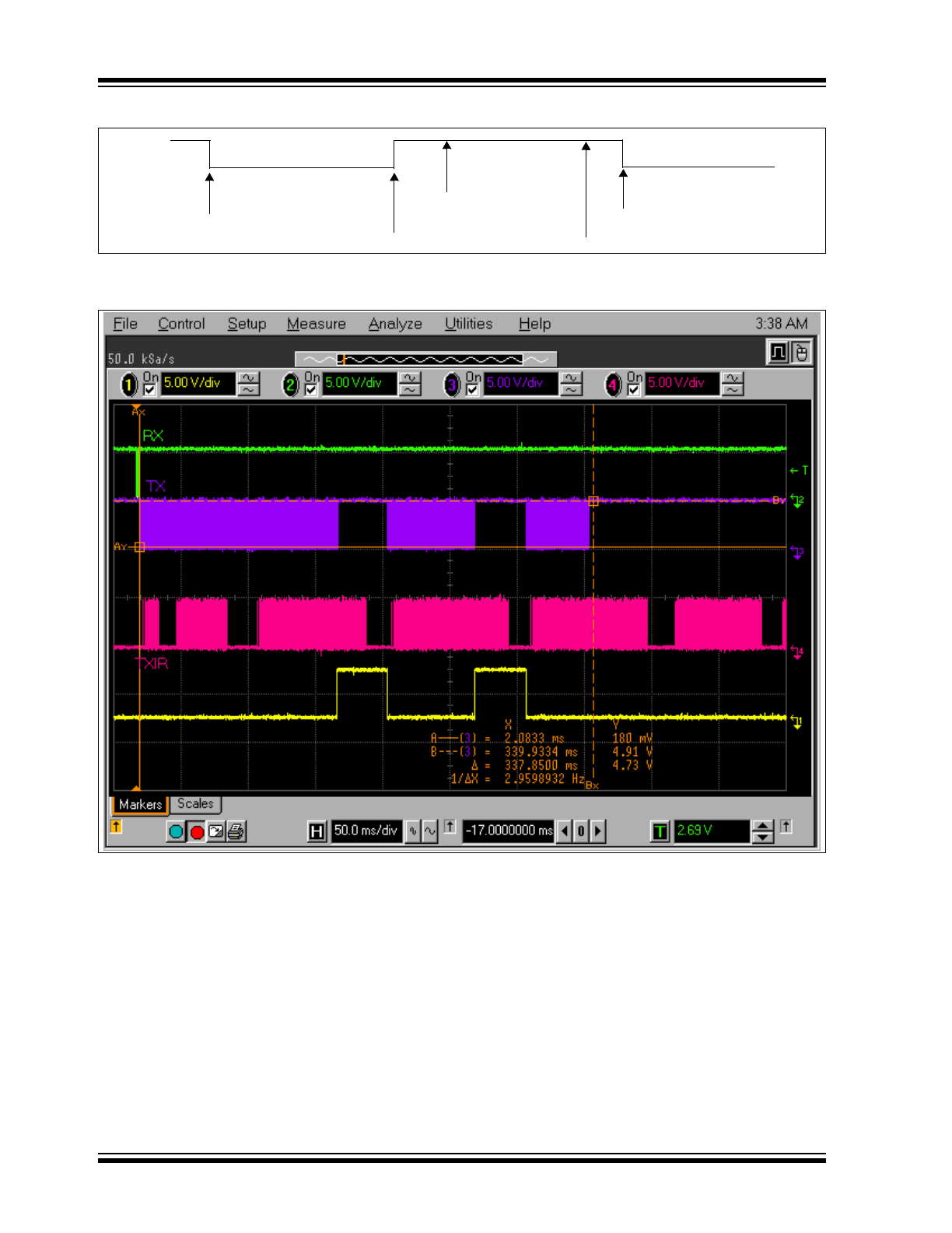
FIGURE 2-3:
HOST UART CTS SIGNAL AND THE RECEIVE BUFFER
FIGURE 2-4:
CTS WAVEFORM FROM HOST CONTROLLER STREAMING OF 250 BYTES TO
THE MCP2140A
CTS
Receive Buffer Empty
MCP2140A Can
Receive Buffer Has 59 Bytes,
Receive Buffer
Receive Buffer Empty
MCP2140A Can Receive Data
IR Data Packet Transmitted
Full (60 Bytes)
CTS Pin Driven High
IR Data Packet Starts Transmission
Receive Data
CTS