
2018 Microchip Technology Inc.
DS20005877A-page 1
HV57908
Features
• 5V CMOS Logic
• Up to 80V Output Voltage
• Low-power Level Shifting
• 8 MHz Data Rate
• Latched Data Outputs
• Forward and Reverse Shifting Options (DIR pin)
• Diode to V
PP
allows Efficient Power Recovery
• Outputs may be Hot Switched
Applications
• Display Driver
• Vacuum Fluorescent Display Driver
• Inkjet Driver
• 3D Printer Driver
• Microelectromechanical Systems Applications
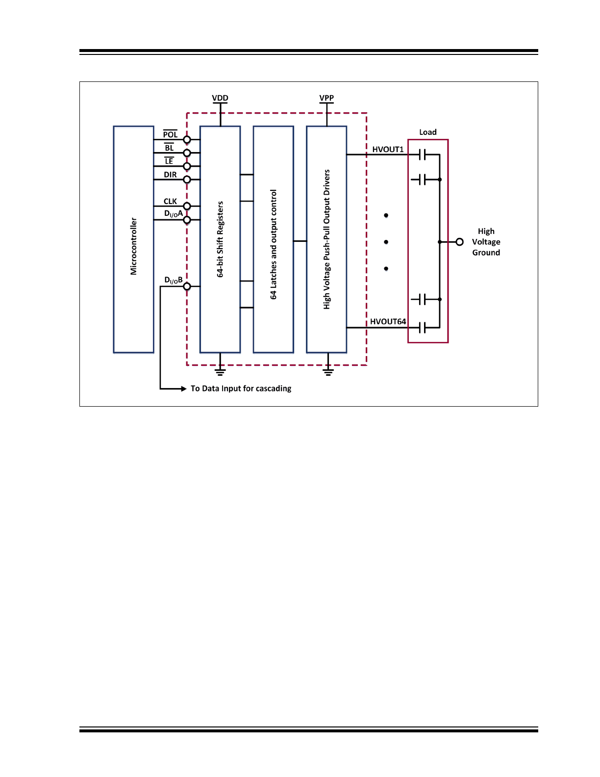
General Description
The HV57908 is a low-voltage to high-voltage
serial-to-parallel converter with 64 push-pull outputs.
This device is designed as a driver for EL displays. It
can also be used in any application requiring
multiple-output high-voltage low-current
sourcing-and-sinking capabilities, such as driving
plasma panels, vacuum fluorescent displays and large
matrix LCD displays.
The device consists of a 64-bit Shift register, 64 latches
and control logic to perform the polarity select and
blanking of the outputs. H
VOUT
1 is connected to the
first stage of the first Shift register through the polarity
and blanking logic. Data is shifted through the Shift
registers on the logic low-to-high transition of the clock.
The DIR pin causes counter-clockwise shifting when
connected to GND and clockwise shifting when
connected to VDD. A data output buffer is provided for
cascading devices. This output reflects the current
status of the last bit of the Shift register, HV
OUT
64. The
operation of the Shift register is not affected by the latch
enable (LE), blanking (BL) and polarity (POL) inputs.
Transfer of data from the Shift registers to the latches
occurs when the LE input is high. The data in the
latches is stored when LE is low.
Package Type
See
Table 2-1
for pin information.
80-lead PQFP
(Top view)
1
80
64-Channel 8 MHz Serial-to-Parallel Converter with Push-Pull Outputs
HV
OUT
2
•
•
•
60 Additional
Outputs
•
•
•
POL
BL
LE
CLK
64 Latches
HV
OUT
63
V
PP
HV
OUT
1
DIR
HV
OUT
64
D
I/O
B
D
I/O
A
64-bit
Static Shift
Register
HV57908
DS20005877A-page 2
2018 Microchip Technology Inc.
Functional Block Diagram
2018 Microchip Technology Inc.
DS20005877A-page 3
HV57908
Typical Application Circuit
HV57908
DS20005877A-page 4
2018 Microchip Technology Inc.
1.0
ELECTRICAL CHARACTERISTICS
Absolute Maximum Ratings†
Supply Voltage, V
DD
............................................................................................................................... –0.5V to +7.5V
Output Voltage, V
PP
................................................................................................................................. –0.5V to +90V
Logic Input Levels ............................................................................................................................ –0.3V to V
DD
+0.3V
Ground Current (
Note 1
) ......................................................................................................................................... 1.5A
Maximum Junction Temperature, T
J(MAX)
........................................................................................................... +125°C
Storage Temperature, T
S
.................................................................................................................... –65°C to +150°C
Continuous Total Power Dissipation:
80-lead PQFP (
Note 2
) ......................................................................................................................... 1200 mW
† Notice: Stresses above those listed under “Absolute Maximum Ratings” may cause permanent damage to the
device. This is a stress rating only, and functional operation of the device at those or any other conditions above those
indicated in the operational sections of this specification is not intended. Exposure to maximum rating conditions for
extended periods may affect device reliability.
Note 1: Limited by the total power dissipated in the package
2: For operations above 25°C ambient, derate linearly to the maximum operating temperature of 70°C
at 20 mW/°C.
RECOMMENDED OPERATING CONDITIONS
Parameter
Sym.
Min.
Typ.
Max.
Unit
Conditions
Logic Supply Voltage
V
DD
4.5
—
5.5
V
Output Voltage
V
PP
8
—
80
V
High-level Input Voltage
V
IH
V
DD
–0.5
—
—
V
Low-level Input Voltage
V
IL
0
—
0.5
V
Clock Frequency per Register
f
CLK
—
—
8
MHz
Operating Ambient Temperature
T
A
–40
—
+85
°C
DC ELECTRICAL CHARACTERISTICS
Electrical Specifications: Over recommended operating conditions unless otherwise noted, T
A
= –40°C to +85°C.
Parameter
Sym.
Min.
Typ.
Max.
Unit
Conditions
V
DD
Supply Current
I
DD
—
—
15
mA
V
DD
= V
DD
maximum,
f
CLK
= 8 MHz
Quiescent V
DD
Supply Current
I
DDQ
—
—
100
µA
All V
IN
= V
DD
High-voltage Supply Current
I
PP
—
—
100
µA
Outputs high
—
—
100
µA
Outputs low
High-level Logic Input Current
I
IH
—
—
1
µA
V
IH
= V
DD
Low-level Logic Input Current
I
IL
—
—
–1
µA
V
IL
= 0V
High-level Output
HV
OUT
V
OH
65
—
—
V
V
PP
= 80V, I
O
= –15 mA
Data Out
V
DD
–0.5
—
—
V
I
O
= –100 µA
Low-level Output
HV
OUT
V
OL
—
—
7
V
V
PP
= 80V, I
O
= 12 mA
Data Out
—
—
0.5
V
I
O
= 100 µA
High-voltage Clamp Diode Voltage
V
OC
—
—
1
V
I
OC
= 1 mA
AC ELECTRICAL CHARACTERISTICS
Electrical Specifications: T
A
= +85°C maximum. Logic signal inputs and data inputs have t
r
, t
f
≤ 5 ns (10% and 90%
points).
Parameter
Sym.
Min.
Typ.
Max.
Unit
Conditions
Clock Frequency
f
CLK
—
—
8
MHz Per register
Clock Width High or Low
t
WL
, t
WH
62
—
—
ns
Data Set-up Time before Clock Rises
t
SU
10
—
—
ns
Data Hold Time after Clock Rises
t
H
15
—
—
ns
Time from Latch Enable to HV
OUT
t
ON
, t
OFF
—
—
500
ns
C
L
= 15 pF
Latch Enable Pulse Width
t
WLE
25
—
—
ns
Delay Time Clock to Latch Enable Low to
High
t
DLE
25
—
—
ns
Note 1
Latch Enable Set-up Time before Clock
Rises
t
SLE
0
—
—
ns
Delay Time Clock to Data Low to High
t
DLH
—
—
70
ns
C
L
= 15 pF
Delay Time Clock to Data High to Low
t
DHL
—
—
70
ns
C
L
= 15 pF
Note 1: t
DLE
is not required but is recommended to produce stable high-voltage outputs and minimize power
dissipation and current spikes. t
DLE
allows the internal SR output to stabilize.
TEMPERATURE SPECIFICATIONS
Parameter
Sym.
Min.
Typ.
Max.
Unit
Conditions
TEMPERATURE RANGE
Operating Ambient Temperature
T
A
–40
—
+85
°C
Maximum Junction Temperature
T
J(MAX)
—
—
+125
°C
Storage Temperature
T
S
–65
—
+150
°C
PACKAGE THERMAL RESISTANCE
80-lead PQFP
JA
—
37
—
°C/W
2018 Microchip Technology Inc.
DS20005877A-page 5
HV57908
HV57908
DS20005877A-page 6
2018 Microchip Technology Inc.
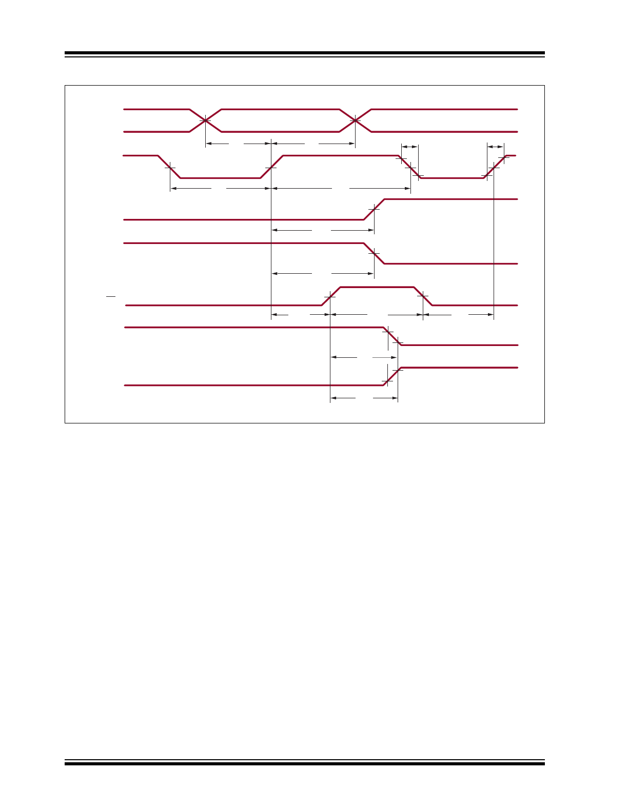
Timing Waveforms
LE
Data Valid
50% 50%
DATA
INPUT
CLK
DATA
OUT
50% 50%
50%
t
SU
t
H
t
WL
t
WH
50%
t
DLH
t
DHL
50%
t
WLE
t
DLE
t
SLE
50%
50%
t
ON
10%
HV
OUT
w/ S/R HIGH
90%
90%
10%
t
OFF
V
IH
V
IL
V
IH
V
IL
V
OH
V
OL
V
OH
V
OL
V
IH
V
IL
V
OH
V
OL
V
OH
V
OL
10%
90%
90%
10% 50%
t
f
t
r
HV
OUT
w/ S/R LOW
2018 Microchip Technology Inc.
DS20005877A-page 7
HV57908
2.0
PIN DESCRIPTION
The details on the pins of HV57908 are listed on
Table 2-1
. Refer to
Package Type
for the location of
pins.
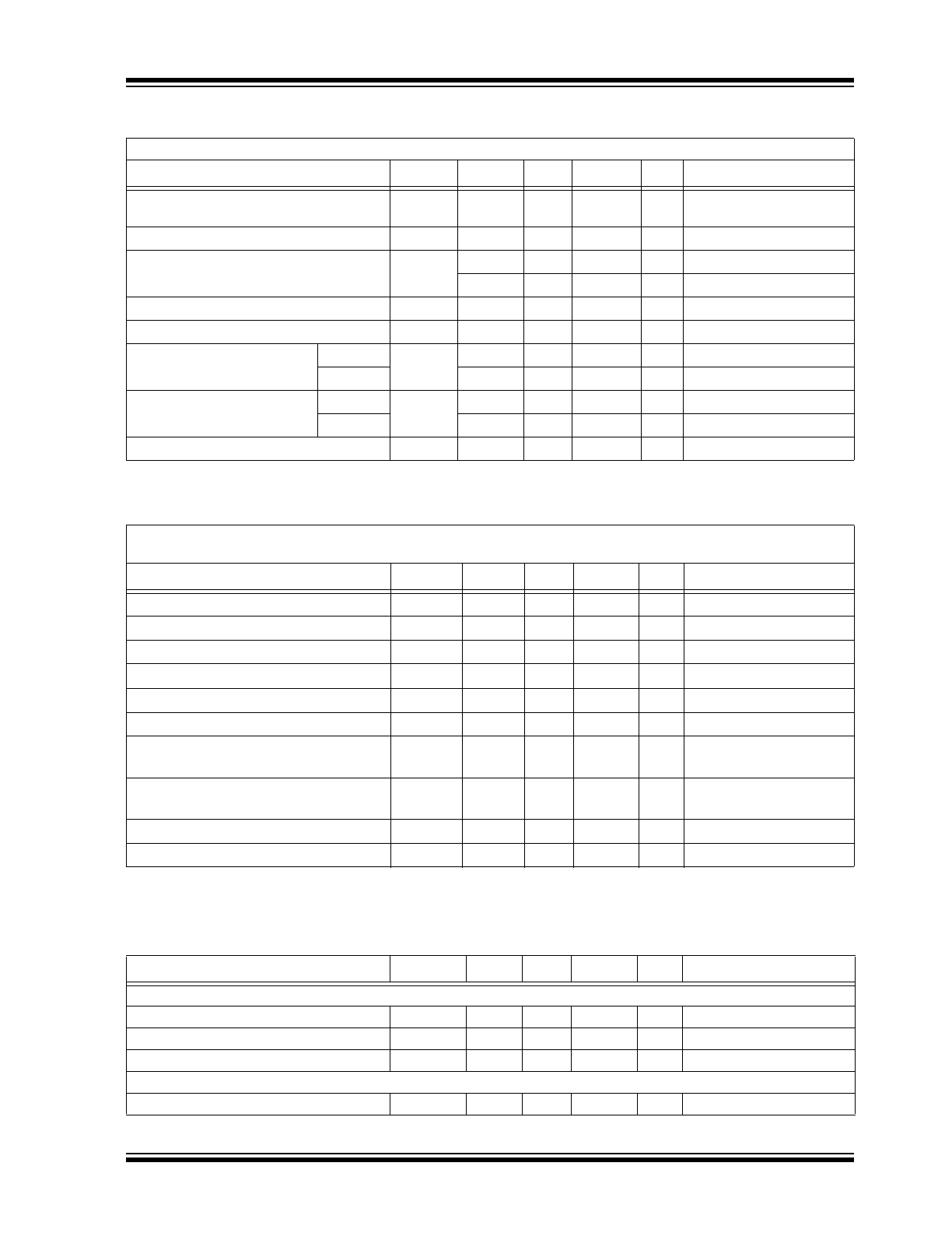
TABLE 2-1:
PIN FUNCTION TABLE
Pin Number
Pin Name
Description
1
HVOUT24/41 High-voltage output
2
HVOUT23/42 High-voltage output
3
HVOUT22/43 High-voltage output
4
HVOUT21/44 High-voltage output
5
HVOUT20/45 High-voltage output
6
HVOUT19/46 High-voltage output
7
HVOUT18/47 High-voltage output
8
HVOUT17/48 High-voltage output
9
HVOUT16/49 High-voltage output
10
HVOUT15/50 High-voltage output
11
HVOUT14/51 High-voltage output
12
HVOUT13/52 High-voltage output
13
HVOUT12/53 High-voltage output
14
HVOUT11/54 High-voltage output
15
HVOUT10/55 High-voltage output
16
HVOUT9/56
High-voltage output
17
HVOUT8/57
High-voltage output
18
HVOUT7/58
High-voltage output
19
HVOUT6/59
High-voltage output
20
HVOUT5/60
High-voltage output
21
HVOUT4/61
High-voltage output
22
HVOUT3/62
High-voltage output
23
HVOUT2/63
High-voltage output
24
HVOUT1/64
High-voltage output
25
DI/OA
Data Input/Output A pin
26
NC
No connection
27
NC
No connection
28
NC
No connection
29
LE
Latch enable pin
30
CLK
Clock pin
31
BL
Blanking pin
32
VDD
Low-voltage supply voltage
33
DIR
Direction pin
34
GND
Ground
Note:
Pin designation for DIR = H/L
Examples: For DIR = H, pin 41 is HVOUT64.
For DIR = L, pin 41 is HVOUT1.
HV57908
DS20005877A-page 8
2018 Microchip Technology Inc.
35
POL
Polarity pin
36
NC
No connection
37
NC
No connection
38
NC
No connection
39
DI/OB
Data Input/Output B pin
40
VPP
High-voltage supply voltage
41
HVOUT64/1
High-voltage output
42
HVOUT63/2
High-voltage output
43
HVOUT62/3
High-voltage output
44
HVOUT61/4
High-voltage output
45
HVOUT60/5
High-voltage output
46
HVOUT59/6
High-voltage output
47
HVOUT58/7
High-voltage output
48
HVOUT57/8
High-voltage output
49
HVOUT56/9
High-voltage output
50
HVOUT55/10 High-voltage output
51
HVOUT54/11 High-voltage output
52
HVOUT53/12 High-voltage output
53
HVOUT52/13 High-voltage output
54
HVOUT51/14 High-voltage output
55
HVOUT50/15 High-voltage output
56
HVOUT49/16 High-voltage output
57
HVOUT48/17 High-voltage output
58
HVOUT47/18 High-voltage output
59
HVOUT46/19 High-voltage output
60
HVOUT45/20 High-voltage output
61
HVOUT44/21 High-voltage output
62
HVOUT43/22 High-voltage output
63
HVOUT42/23 High-voltage output
64
HVOUT41/24 High-voltage output
65
HVOUT40/25 High-voltage output
66
HVOUT39/26 High-voltage output
67
HVOUT38/27 High-voltage output
68
HVOUT37/28 High-voltage output
69
HVOUT36/29 High-voltage output
70
HVOUT35/30 High-voltage output
71
HVOUT34/31 High-voltage output
72
HVOUT33/32 High-voltage output
73
HVOUT32/33 High-voltage output
TABLE 2-1:
PIN FUNCTION TABLE (CONTINUED)
Pin Number
Pin Name
Description
Note:
Pin designation for DIR = H/L
Examples: For DIR = H, pin 41 is HVOUT64.
For DIR = L, pin 41 is HVOUT1.
2018 Microchip Technology Inc.
DS20005877A-page 9
HV57908
74
HVOUT31/34 High-voltage output
75
HVOUT30/35 High-voltage output
76
HVOUT29/36 High-voltage output
77
HVOUT28/37 High-voltage output
78
HVOUT27/38 High-voltage output
79
HVOUT26/39 High-voltage output
80
HVOUT25/40 High-voltage output
TABLE 2-1:
PIN FUNCTION TABLE (CONTINUED)
Pin Number
Pin Name
Description
Note:
Pin designation for DIR = H/L
Examples: For DIR = H, pin 41 is HVOUT64.
For DIR = L, pin 41 is HVOUT1.
HV57908
DS20005877A-page 10
2018 Microchip Technology Inc.
3.0
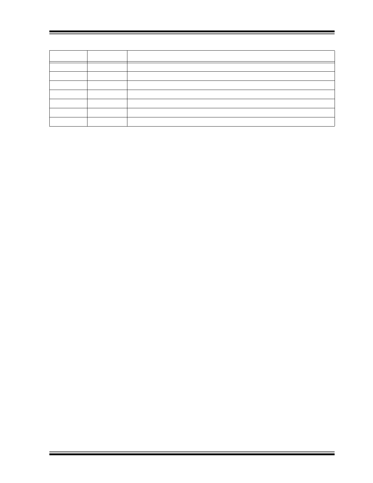
FUNCTIONAL DESCRIPTION
Follow the steps in
Table 3-1
to power up and power
down the HV57908.
TABLE 3-1:
POWER-UP AND POWER-DOWN SEQUENCE
Power-up
Power-down
Step
Description
Step
Description
1
Connect ground.
1
Remove V
PP.
(
Note 1
)
2
Apply V
DD.
2
Remove all inputs.
3
Set all inputs (Data, CLK, Enable, etc.) to a known state.
3
Remove V
DD.
4
Apply V
PP.
(
Note 1
)
4
Disconnect ground.
Note 1: The V
PP
should not drop below V
DD
or float during operation.
TABLE 3-2:
Function
Inputs
Outputs
Data
CLK
LE
BL
POL DIR Shift Register
High-voltage Output
Data Out
All O/P High
X
X
X
L
L
X
—
H
—
All O/P Low
X
X
X
L
H
X
—
L
—
O/P Normal
X
X
X
H
H
X
—
No inversion
—
O/P Inverted
X
X
X
H
L
X
—
Inversion
—
Data Falls through
Latches (Latches
Transparent)
L
↑
H
H
H
X
L
L
—
H
↑
H
H
H
X
H
H
—
L
↑
H
H
L
X
L
H
—
H
↑
H
H
L
X
H
L
—
Data
Stored/Latches
Loaded
X
X
L
H
H
X
*
Stored data
—
X
X
L
H
L
X
*
Inversion of stored data
—
I/O Relation
D
I/OA
↑
X
X
X
H
Q
N
→Q
N+1
—
D
I/OB
D
I/OB
↑
X
X
X
L
Q
N
→Q
N–1
—
D
I/OA
Note:
H = High-logic level
L = Low-logic level
X = Irrelevant
↑ = Low-to-high transition
* = Dependent on the previous stage’s state
TRUTH FUNCTION TABLE
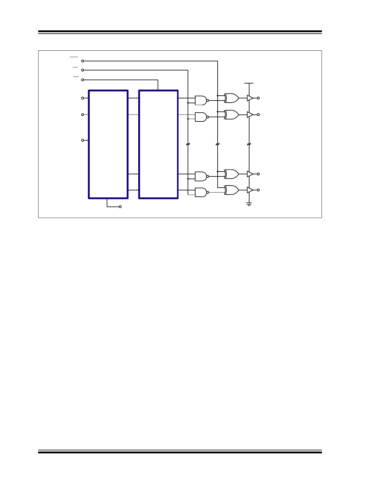
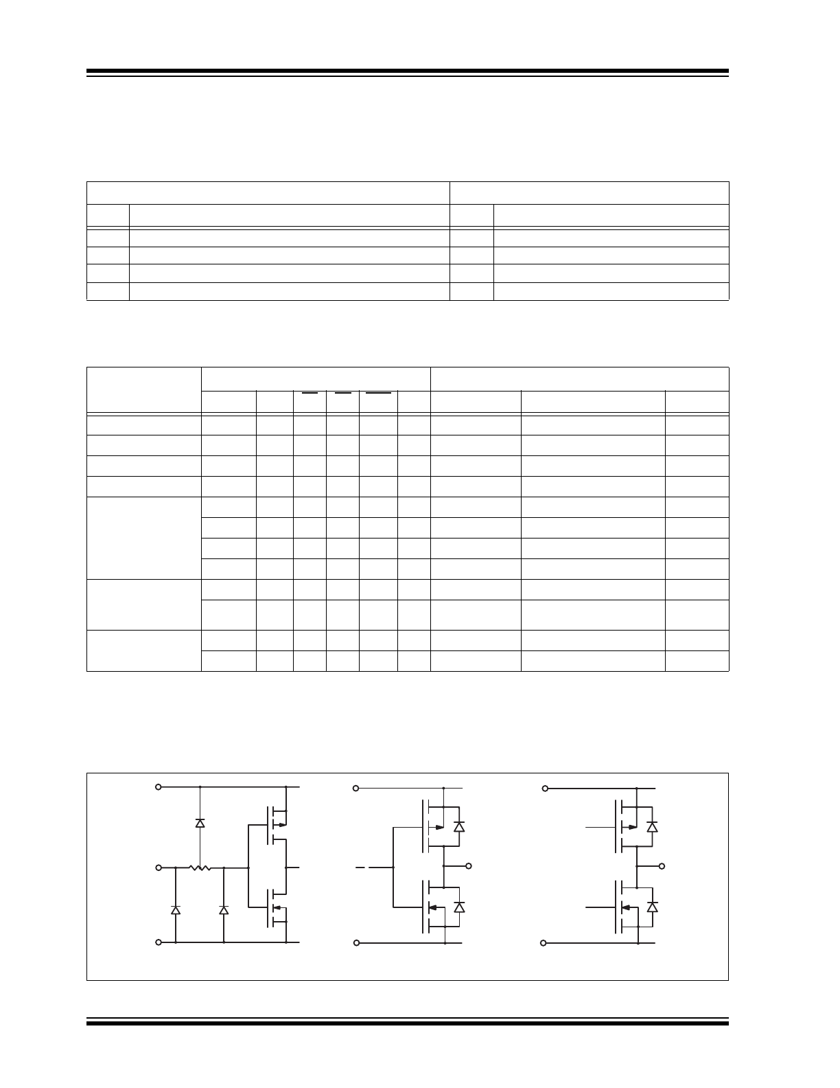
VDD
INPUT
DATA
GND
VPP
GND
HV
OUT
Logic Inputs
GND
DATA
OUTPUT
Logic Data Output
High Voltage Outputs
VDD
FIGURE 3-1:
Input and Output Equivalent Circuits.