
2017 Microchip Technology Inc.
DS20005832A-page 1
HV264
Features
• Four Independent High-voltage Amplifiers
• 190V Output Swing
• 9V/µs Typical Output Slew Rate
• 66.7V/V Fixed Gain
• High-value Internal Feedback Resistors
• Very Low Operating Current
Applications
• Tunable Laser
• Microelectromechanical Systems (MEMS) Driver
• Test Equipment
• Piezoelectric Transducer Driver
• Braille Driver
General Description
The HV264 is a quad high-voltage amplifier array
integrated circuit. It operates on a 200V high-voltage
supply and a 5V low-voltage supply. Each channel has
its own input and output.
When both V
OUT
and FB pins are connected together
and RGND is set at 0V, a non-inverting amplifier is
formed with a closed-loop gain of 66.7V/V. High-value
internal feedback resistors are used to minimize power
dissipation. The input voltage V
IN
is designed for a
range of 0.05V to 2.85V. The output can swing from 1V
to V
PP
–10V. A 2.85V input will cause the output to
swing to 190V.
The HV264 is designed for maximum performance with
minimal high-voltage current. The high-voltage current
for each channel is less than 75 µA. The typical output
slew rate performance is 9V/µs.
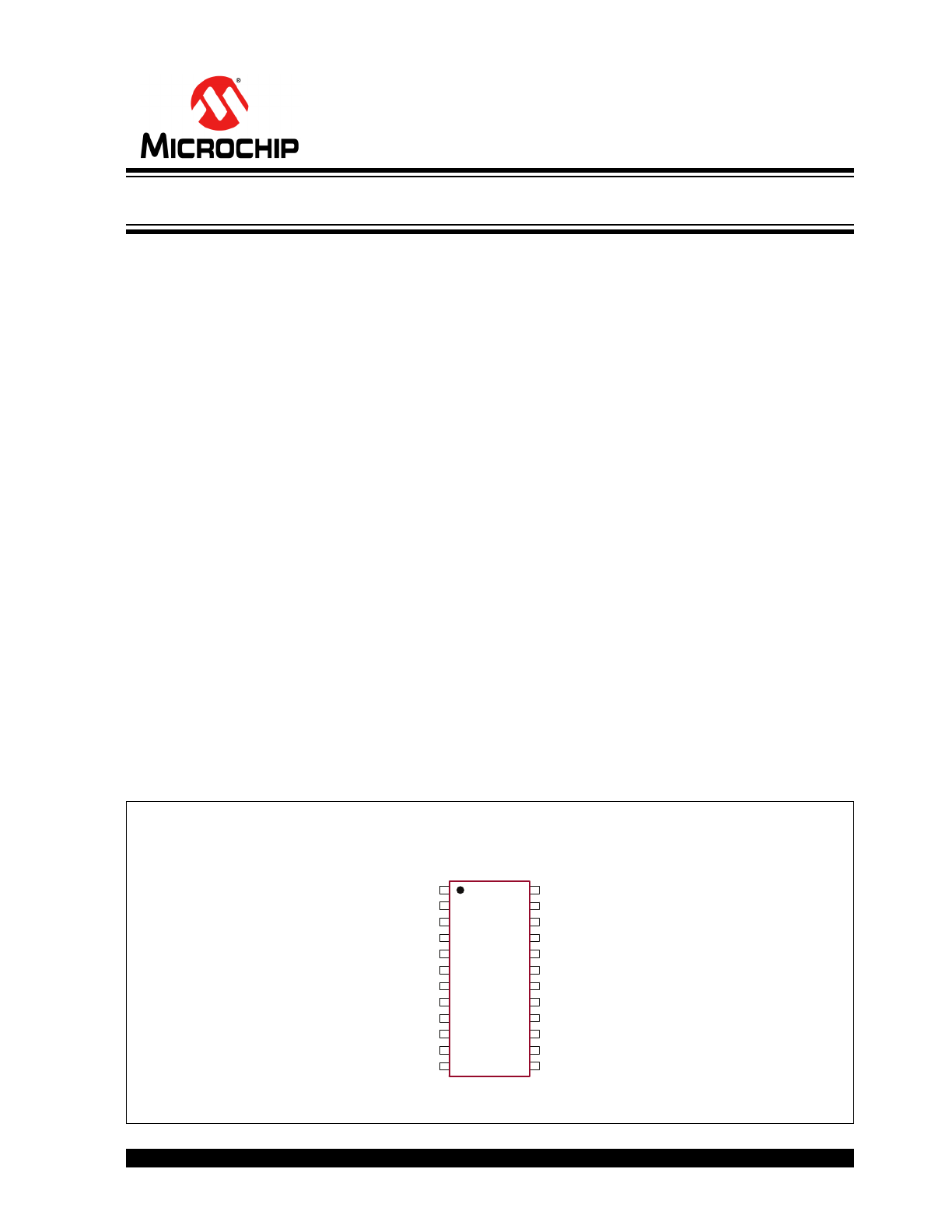
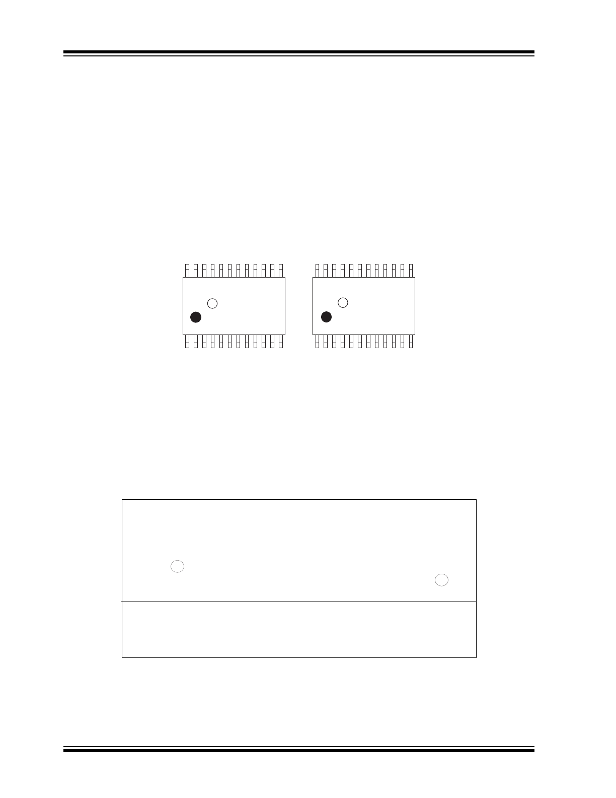
Package Type
24-lead TSSOP
(Top view)
See
Table 3-1
for pin information.
1
NC
HV
OUT
1
FB1
HV
OUT
2
FB2
VPP
HVGND
HV
OUT
3
FB3
HV
OUT
4
FB4
NC
NC
VIN1
RGND1
VIN2
RGND2
VDD
GND
VIN3
RGND3
VIN4
RGND4
NC
24
Quad High-Voltage Amplifier Array
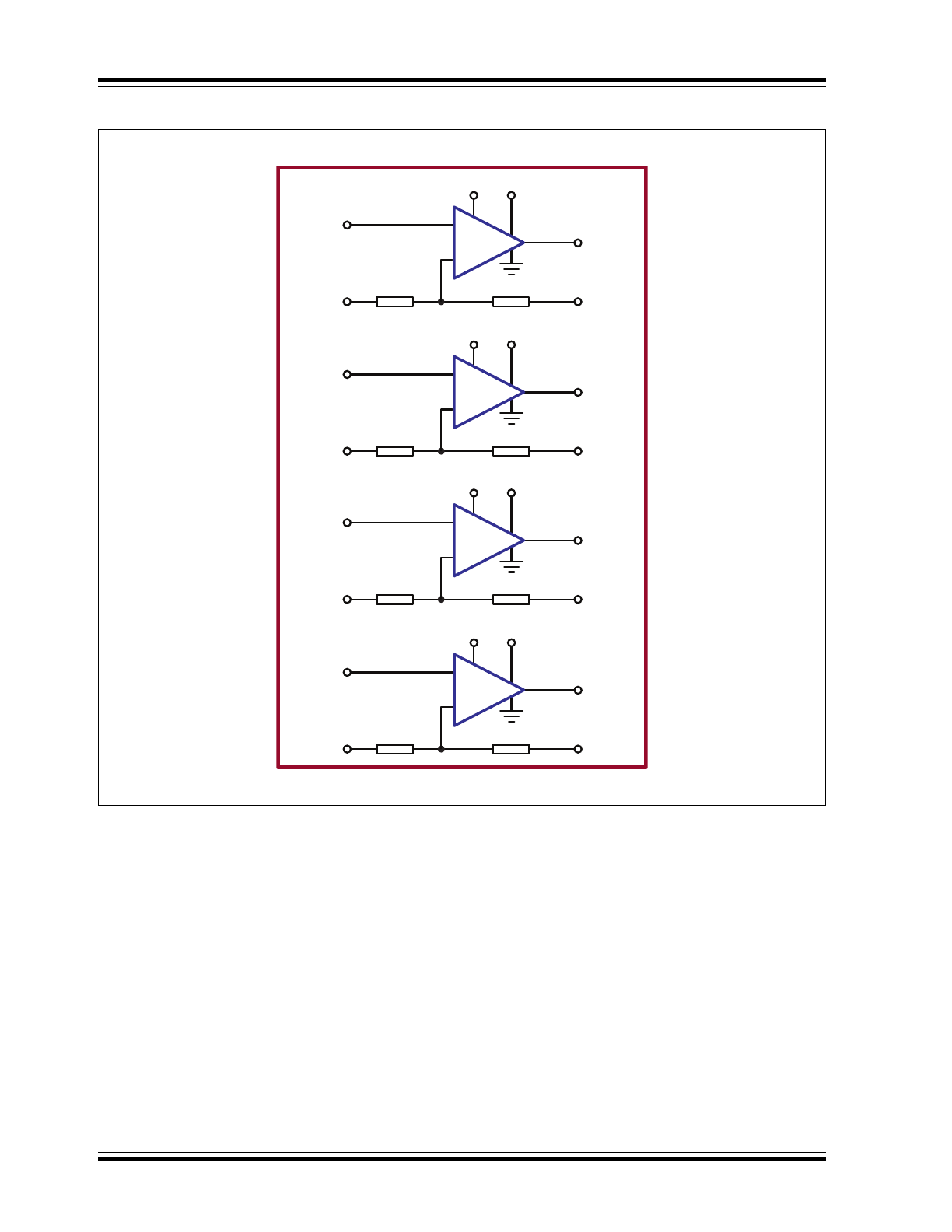
VDD VPP
VDD VPP
VDD VPP
VDD VPP
VIN1
RGND1
VIN2
RGND2
VIN3
RGND3
VIN4
RGND4
R 65.7R
R 65.7R
R 65.7R
R 65.7R
VOUT1
FB1
VOUT2
FB2
VOUT3
FB3
VOUT4
FB4
+
-
+
-
+
-
+
-
HV264
DS20005832A-page 2
2017 Microchip Technology Inc.
Functional Block Diagram
2017 Microchip Technology Inc.
DS20005832A-page 3
HV264
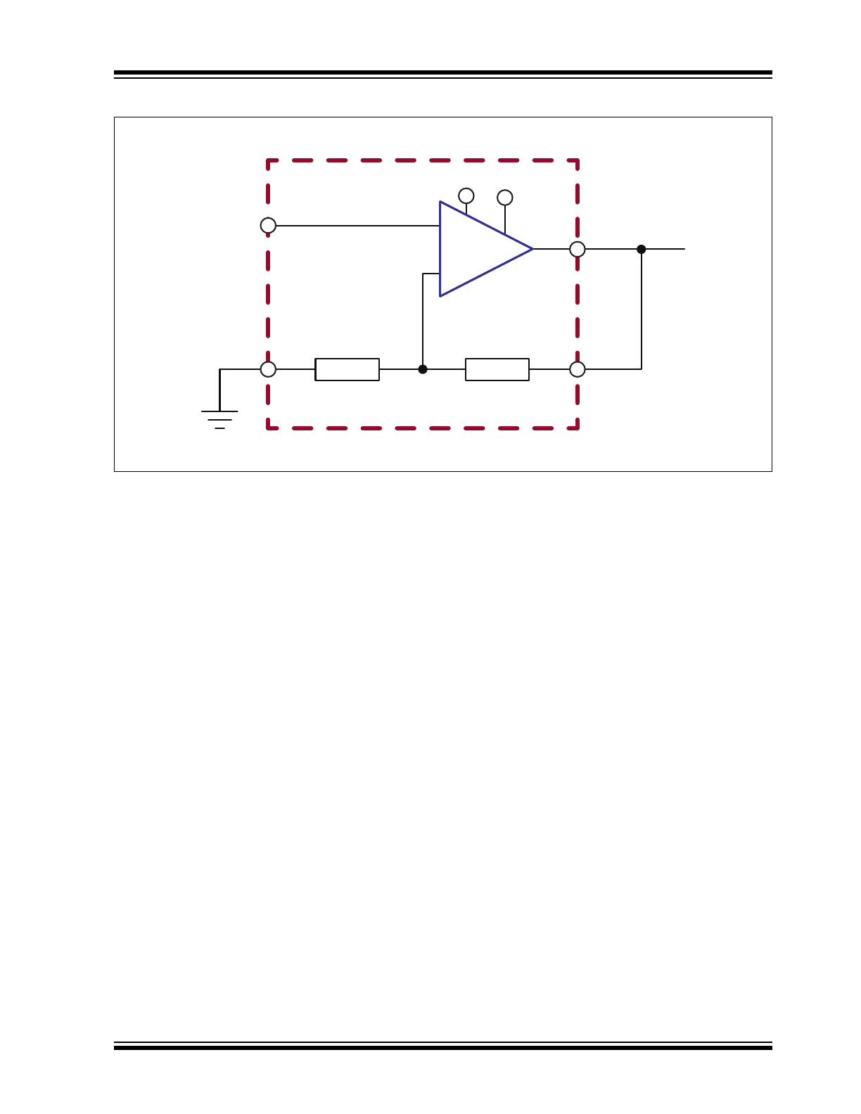
Typical Application Circuit
+
-
HV264
HVOUT
FB
VDD VPP
VIN
RGND
R
kR
HV264
DS20005832A-page 4
2017 Microchip Technology Inc.
1.0
ELECTRICAL CHARACTERISTICS
Absolute Maximum Ratings†
High-voltage Supply, V
PP
....................................................................................................................................... 225V
Low-voltage Supply, V
DD
......................................................................................................................................... 6.5V
Output Voltage, HV
OUT
................................................................................................................................... 0V to V
PP
Analog Input Signal, V
IN
................................................................................................................................. 0V to V
DD
Maximum Junction Temperature, T
J
.................................................................................................................... 150°C
Storage Temperature, T
S
.................................................................................................................... –65°C to +150°C
ESD Rating (
Note 1
) ............................................................................................................................... ESD Sensitive
† Notice: Stresses above those listed under “Absolute Maximum Ratings” may cause permanent damage to the
device. This is a stress rating only, and functional operation of the device at those or any other conditions above those
indicated in the operational sections of this specification is not intended. Exposure to maximum rating conditions for
extended periods may affect device reliability.
Note 1: Device is ESD sensitive. Handling precautions are recommended.
RECOMMENDED OPERATING CONDITIONS
Parameter
Sym.
Min.
Typ.
Max.
Unit
Conditions
High-voltage Positive Supply
V
PP
50
—
200
V
Low-voltage Positive Supply
V
DD
4.5
5
5.5
V
Input Ground Range
R
GND
0
0
V
DD
V
V
PP
Supply Current
I
PP
—
—
300
µA
V
PP
= 200V, all inputs at 0V
V
DD
Supply Current
I
DD
—
—
5
mA
V
DD
= 5.5V
Operating Ambient Temperature
T
A
–40
—
85
°C
Operating Junction Temperature
T
J
–40
—
100
°C

DC ELECTRICAL CHARACTERISTICS
Electrical Specifications: Over operating conditions unless otherwise noted, T
J
= 25°C.
Parameter
Sym.
Min.
Typ.
Max.
Unit
Conditions
HV
OUT
Voltage Swing
HV
OUT
1
—
V
PP
–10
V
No load
HV
OUT
Sink Current
I
SINK
3
—
—
mA
HV
OUT
Source Current
I
SOURCE
3
—
—
mA
Input Voltage Range
V
IN
0
—
V
DD
–1.5
V
V
IN
Input Current
I
IN
—
—
50
nA
H
VOUT
DC Offset
HV
OS
—
—
±1
V
V
IN
= 0.2V
AC ELECTRICAL CHARACTERISTICS
Electrical Specifications: Over operating conditions unless otherwise noted, T
J
= 25°C.
Parameter
Sym.
Min.
Typ.
Max.
Unit
Conditions
HV
OUT
Slew Rate–Rising Edge
SR
5
9
30
V/µs
V
PP
= 200V,
Load = 15 pF,
measured between
10% to 90% of HV
OUT
HV
OUT
Slew Rate–Falling Edge
—
9
—
V/µs
Feedback Impedance, R
f
+ R
i
R
FB
3.5
5.3
—
MΩ
Closed-loop Gain
A
V
63.4
66.7
70
V/V
HV
OUT
–3 dB Channel Bandwidth
BW
25
—
—
kHz
V
PP
= 200V,
Load = 15 pF
HV
OUT
Capacitive Load
C
LOAD
0
—
15
pF
Output Referred Noise
V
N
—
—
10
mV
RMS
Measured at HV
OUT
,
0 kHz to 1 kHz single
pole, V
IN
= 0.2V
V
DD
Power Supply Rejection Ratio
PSRR1
55
—
—
dB
V
DD
= 4.5V to 5.5V
V
PP
= 200V,
V
IN
= 0.1V
V
PP
Power Supply Rejection Ratio
PSRR2
60
—
—
dB
V
DD
= 5V,
V
PP
= 50V to 200V,
V
IN
= 0.1V
Crosstalk
Xtalk
—
—
–80
dB
Output referred
TEMPERATURE SPECIFICATIONS
Parameter
Sym.
Min.
Typ.
Max.
Unit
Conditions
TEMPERATURE RANGE
Operating Ambient Temperature
T
A
–40
—
85
°C
Operating Junction Temperature
T
J
–40
—
100
°C
Storage Temperature
T
S
–65
—
150
°C
PACKAGE THERMAL RESISTANCE
24-lead TSSOP
JA
—
72
—
°C/W
2017 Microchip Technology Inc.
DS20005832A-page 5
HV264
HV264
DS20005832A-page 6
2017 Microchip Technology Inc.
2.0
TYPICAL PERFORMANCE CURVES
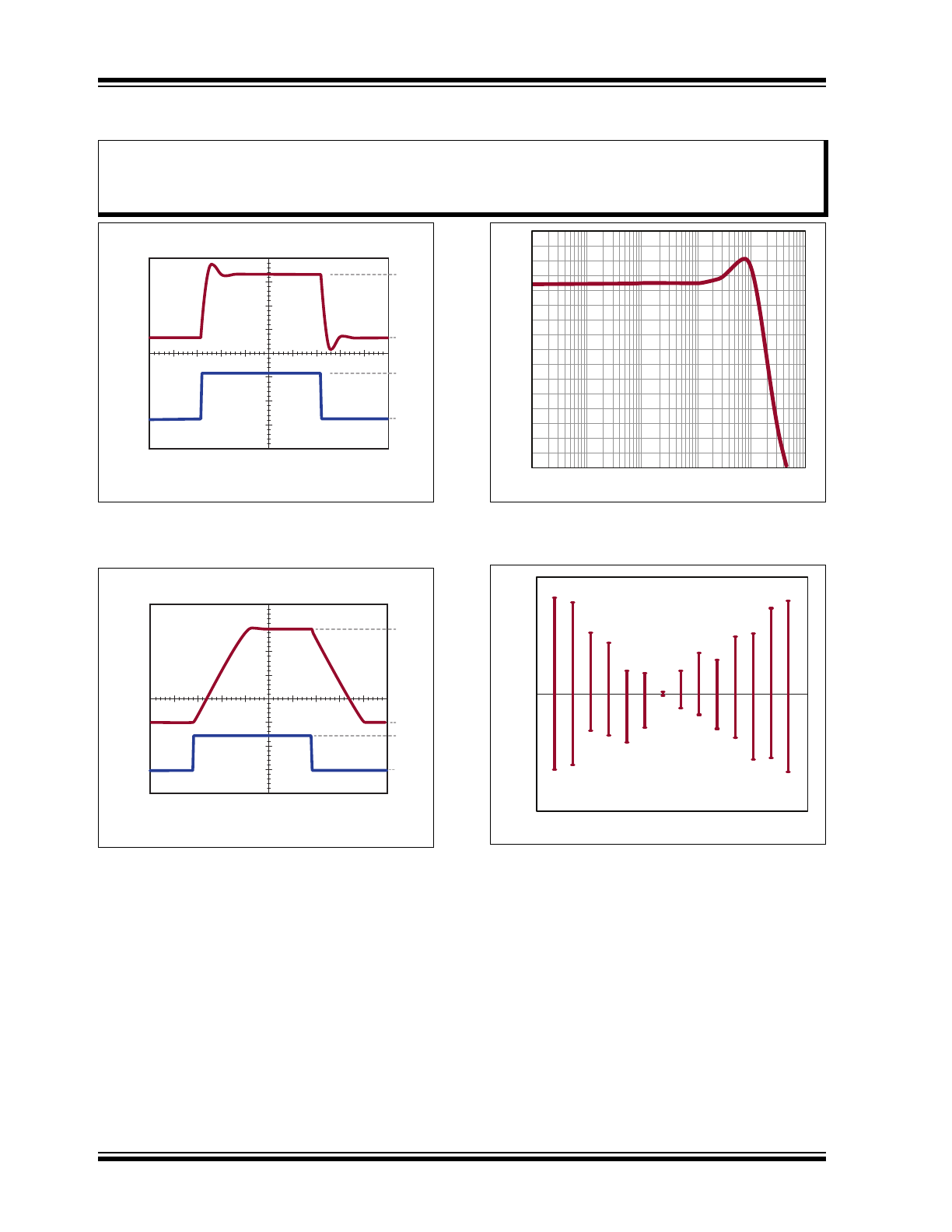
133V
100V
1.70V
1.5V
HV
OUT
Output
V
IN
Input
10µ/div
Note:
The graphs and tables provided following this note are a statistical summary based on a limited number of
samples and are provided for informational purposes only. The performance characteristics listed herein
are not tested or guaranteed. In some graphs or tables, the data presented may be outside the specified
operating range (e.g. outside specified power supply range) and therefore outside the warranted range.
FIGURE 2-1:
Typical Small-signal Pulse
Response.
190V
0V
2.85V
0V
HV
OUT
Output
V
IN
Input
10µ/div
FIGURE 2-2:
Typical Large-signal Pulse
Response.
FIGURE 2-3:
Typical Bode Plot of Small-
signal Gain
40
35
30
25
Signal (dB)
Frequency (Hz)
10 100 1000 10000 100000 1000000
(V
IN
= 0.2 V
P–P
, V
DC
= 1.5V,
V
DD
= 5V and V
PP
= 200V).
50
40
30
20
10
0
-10
-20
-30
-40
-50
Voltage (mV)
-50 -40 -30 -20 -10 0 10 20 30 40 50 60 70 80 90 100
Temperature (°C)
FIGURE 2-4:
Distribution of Typical
HV
OUT
Deviation over Temperature
(V
IN
= 0.1 V
DC
, 1.6 V
DC
, 3.3 V
DC
, in reference
to 20°C).
2017 Microchip Technology Inc.
DS20005832A-page 7
HV264
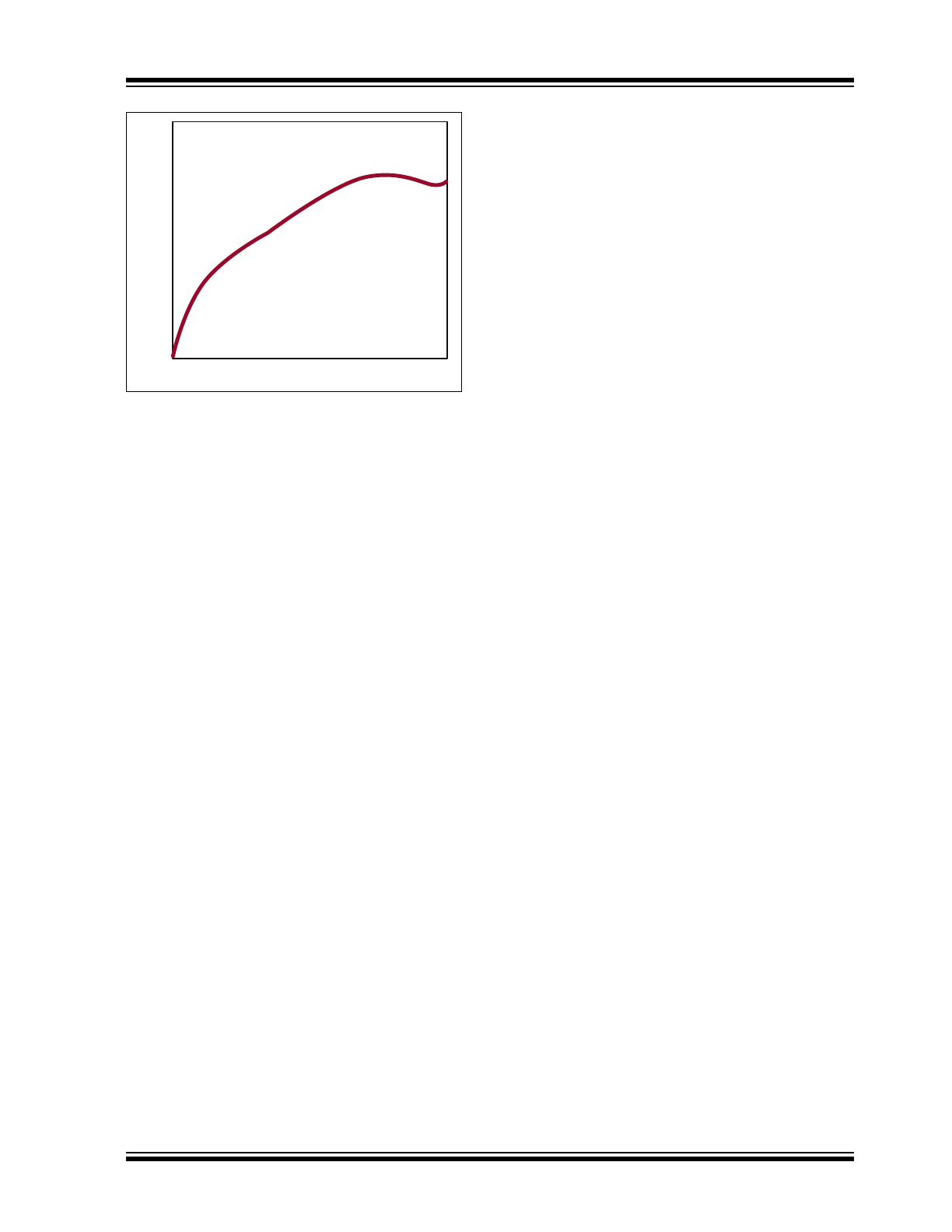
FIGURE 2-5:
70
60
50
40
30
20
10
0
Voltage (mV)
Time (hour)
0 1 2 3 4 5
Typical HV
OUT
Drift Over
Time (V
PP
= 200V, V
DD
= 5.5V, V
IN
= 0.2V, Room
Temperature and 50 pF Output Loading).
HV264
DS20005832A-page 8
2017 Microchip Technology Inc.
3.0
PIN DESCRIPTION
The details on the pins of HV264 are listed on
Table 3-1
. Refer to
Package Type
for the location of
pins.
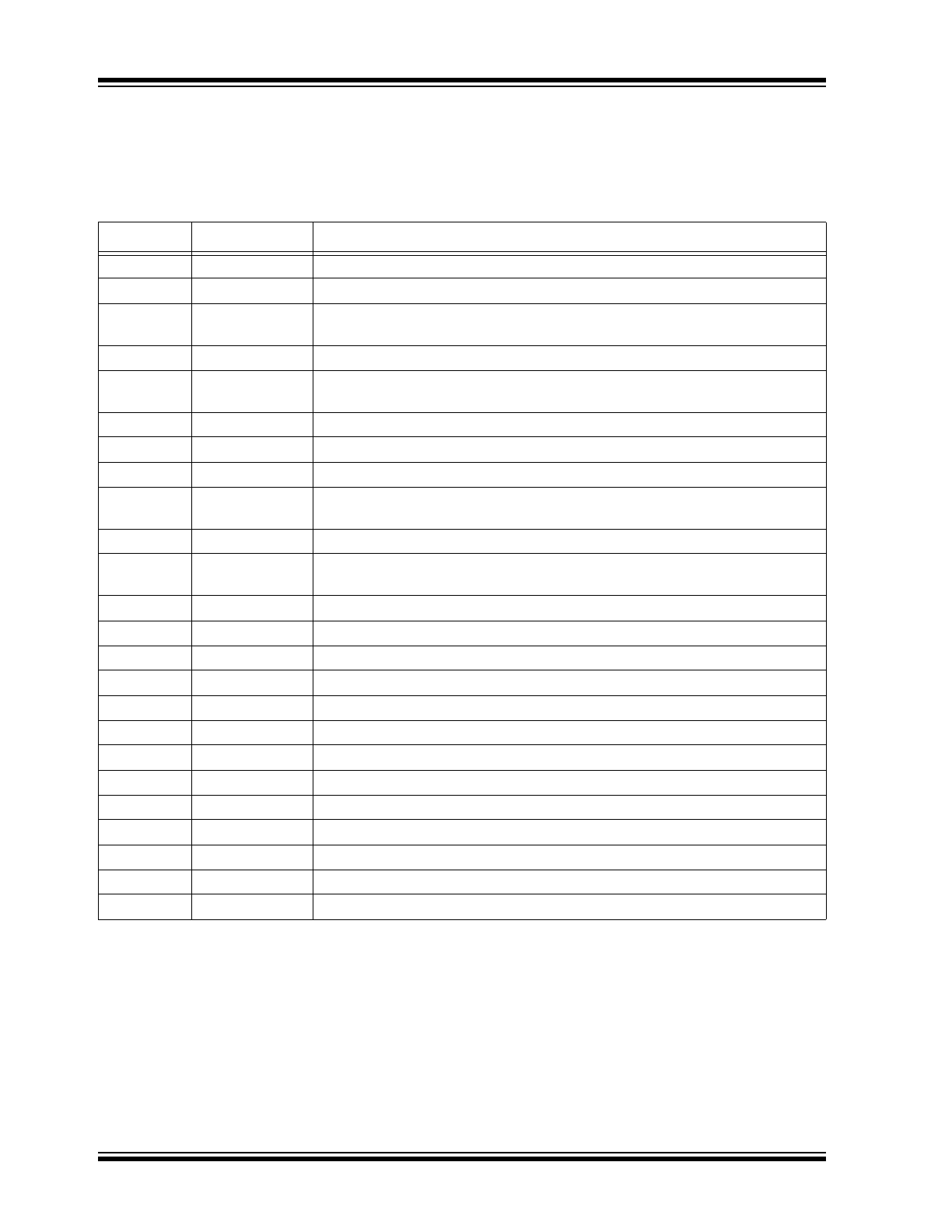
TABLE 3-1:
PIN FUNCTION TABLE
Pin Number
Pin Name
Description
1
NC
No connection
2
VIN1
Amplifier Input 1
3
RGND1
Resistor ground for Channel 1. Typically grounded. Can be connected to a
voltage source to create a DC offset.
4
VIN2
Amplifier Input 2
5
RGND2
Resistor ground for Channel 2. Typically grounded. Can be connected to a
voltage source to create a DC offset.
6
VDD
Low-voltage positive supply
7
GND
Device ground
8
VIN3
Amplifier Input 3
9
RGND3
Resistor ground for Channel 3. Typically grounded. Can be connected to a
voltage source to create a DC offset.
10
VIN4
Amplifier Input 4
11
RGND4
Resistor ground for Channel 4. Typically grounded. Can be connected to a
voltage source to create a DC offset.
12
NC
No connection
13
NC
No connection
14
FB4
Feedback Input 4
15
HVOUT4
Amplifier Output 4
16
FB3
Feedback Input 3
17
HVOUT3
Amplifier Output 3
18
HVGND
Device high-voltage supply ground
19
VPP
High-voltage positive supply
20
FB2
Feedback Input 2
21
HVOUT2
Amplifier Output 2
22
FB1
Feedback Input 1
23
HVOUT1
Amplifier Output 1
24
NC
No connection
2017 Microchip Technology Inc.
DS20005832A-page 9
HV264
4.0
FUNCTIONAL DESCRIPTION
4.1
Power-up/Power-down Sequence
The device can be damaged due to improper power-
up/power-down sequence. To avoid this, please follow
the acceptable power-up and power-down sequences
in
Table 4-1
and
Table 4-2
and add an external diode
across V
PP
and V
DD
where the anode of the diode is
connected to V
DD
and the cathode of the diode is
connected to V
PP
. Any low-current high-voltage diode
such as a 1N4004 will be adequate.
TABLE 4-1:
ACCEPTABLE POWER-UP SEQUENCES
Option 1
Option 2
Step
Description
Step
Description
1
V
DD
1
V
DD
2
V
PP
2
Inputs
3
Inputs
3
V
PP
TABLE 4-2:
ACCEPTABLE POWER-DOWN SEQUENCES
Option 1
Option 2
Step
Description
Step
Description
1
Inputs
1
V
PP
2
V
PP
2
Inputs
3
V
DD
3
V
DD
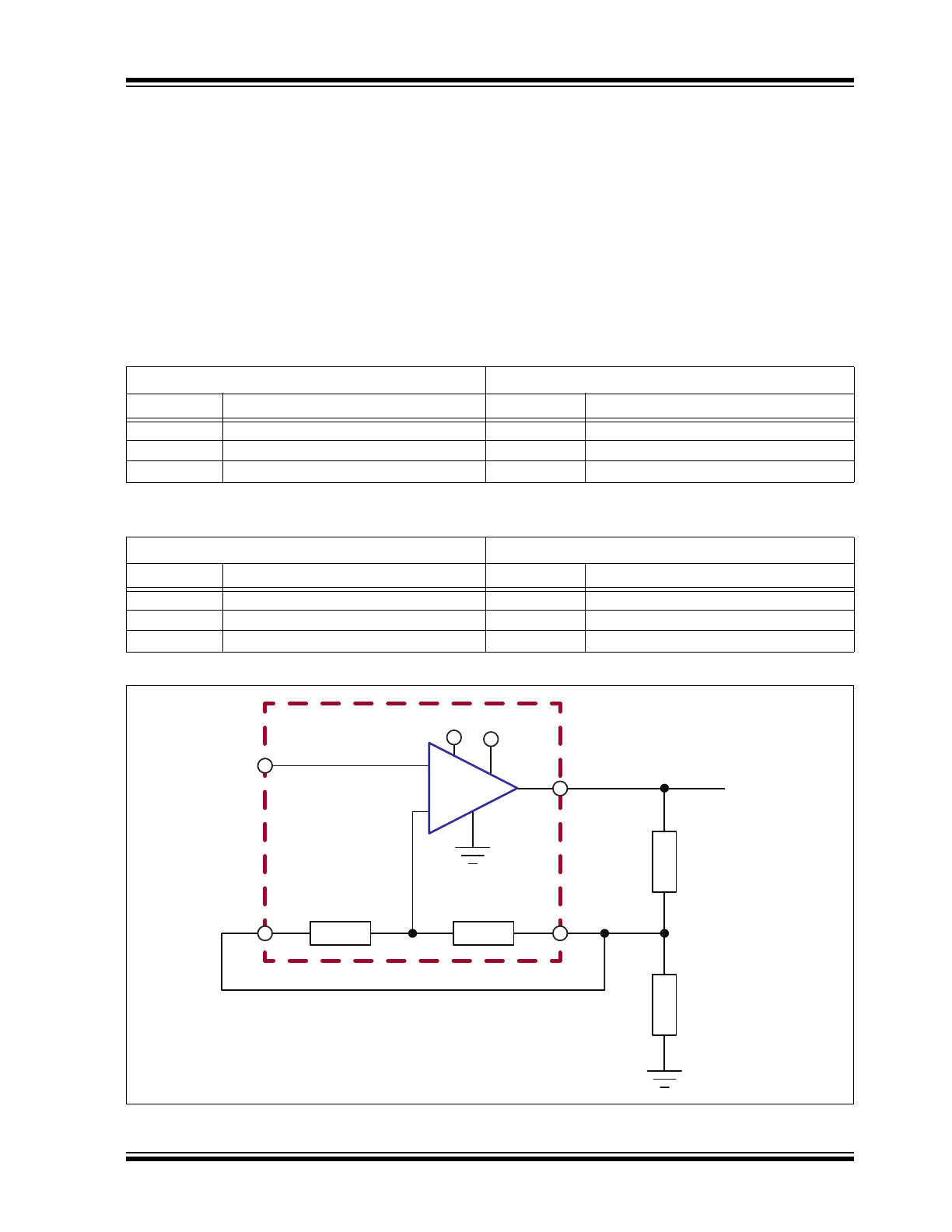
+
-
HV264
HVOUT
FB
VDD VPP
VIN
RGND
R
kR
Rf
Rg
Rf and Rg
are external
resistors
Closed loop gain
must be greater
than 66.7V/V
FIGURE 4-1:
Application Circuit with External Gain Setting Resistors.
HV264
DS20005832A-page 10
2017 Microchip Technology Inc.
5.0
PACKAGE MARKING INFORMATION
5.1
Packaging Information
Legend: XX...X
Product Code or Customer-specific information
Y
Year code (last digit of calendar year)
YY
Year code (last 2 digits of calendar year)
WW
Week code (week of January 1 is week ‘01’)
NNN
Alphanumeric traceability code
Pb-free JEDEC
®
designator for Matte Tin (Sn)
*
This package is Pb-free. The Pb-free JEDEC designator ( )
can be found on the outer packaging for this package.
Note:
In the event the full Microchip part number cannot be marked on one line, it will
be carried over to the next line, thus limiting the number of available
characters for product code or customer-specific information. Package may or
not include the corporate logo.
3
e
3
e
434
HV264
1725
e3
NNN
XXXXXXX
YYWW
e3
24-lead TSSOP
Example
TS
XX