
2009-2017 Microchip Technology Inc.
DS00002444A-page 1
General Description
The CAP1114, which incorporates Microchip’s Right-
Touch
TM
technology, is a multiple channel Capacitive
Touch sensor and LED Driver.
The CAP1114 contains up to fourteen (14) individual
Capacitive Touch sensor inputs with programmable
sensitivity for use in touch button and slider switch
applications. Each sensor also contains automatic
recalibration with programmable time delays.
The CAP1114 also includes internal circuitry to com-
pensate for design and parasitic variance in un-
touched capacitance on sensors.
The CAP1114 also contains eleven (11) low side LED
drivers that offer full-on / off, variable rate blinking, dim-
ness controls, and breathing. Capacitive buttons can
be linked to LED outputs.
Applications
• Consumer Electronics
• Desktop and Notebook PCs
• LCD Monitors
Features
• Fourteen (14) capacitive touch sensor inputs
- Compensates for variable sensor capaci-
tance
- Programmable sensitivity
- High SNR allows for easy tuning
- Automatic recalibration
- Slider acceleration detection
- Slider positional detection
- Proximity detection
• Lid closure detection
• Low power operation
- 4.5uA quiescent current in Deep Sleep
- 200uA quiescent current in Sleep while moni-
toring 1 button
• Alert to signal touch to host processor
• User controlled reset
• Low external component count
• SMBus 2.0 compliant interface to change operat-
ing parameters to work in a wide variety of sys-
tems
- Block Read and Write function for quick task-
ing
• Eleven (11) LED driver outputs
- Programmable blink, breathe, and dimness
controls
- 8 configurable as GPIOs
- Buttons can be linked to LED responses
• Development boards and software available
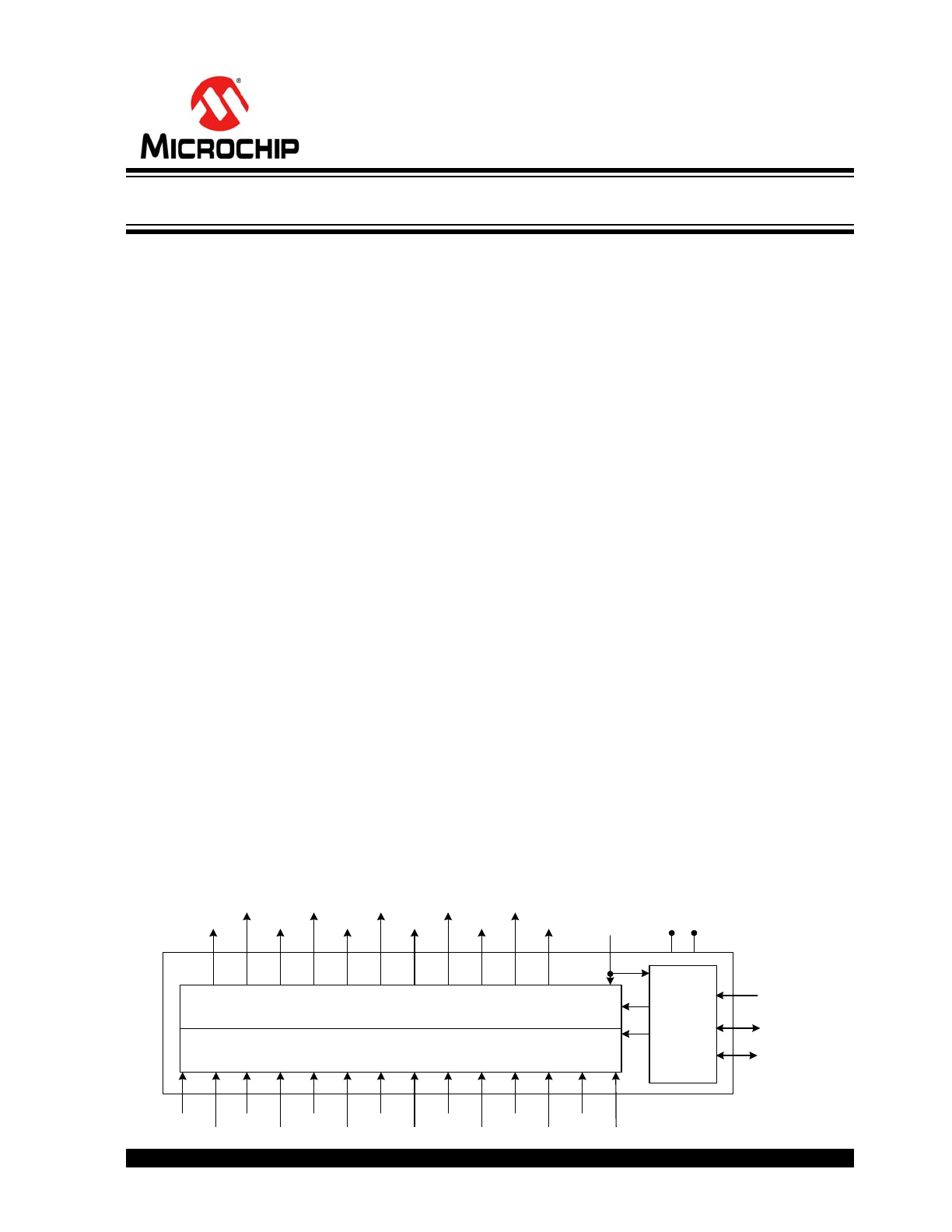
Block Diagram
SMBus
Slave
Protocol
SMCLK
SMDATA
VDD
GND
ALERT
Capacitive Sensing Algorithm
LED Blink, Breathe, and Dimness control
LED1
LED2
LED3
LED4
LED5
LED6
LED7
LED8
LED9
LED10
LED11
CS1
CS2
CS3
CS4
CS5
CS6
CS7
CS8
CS9
CS10
CS11
CS12
CS13
CS14
RESET
CAP1114
Multiple Channel Capacitive Touch Sensor and LED Driver

CAP1114
DS00002444A-page 2
2009-2017 Microchip Technology Inc.
TO OUR VALUED CUSTOMERS
It is our intention to provide our valued customers with the best documentation possible to ensure successful use of your Microchip
products. To this end, we will continue to improve our publications to better suit your needs. Our publications will be refined and
enhanced as new volumes and updates are introduced.
If you have any questions or comments regarding this publication, please contact the Marketing Communications Department via
E-mail at
docerrors@microchip.com
. We welcome your feedback.
Most Current Data Sheet
To obtain the most up-to-date version of this data sheet, please register at our Worldwide Web site at:
http://www.microchip.com
You can determine the version of a data sheet by examining its literature number found on the bottom outside corner of any page.
The last character of the literature number is the version number, (e.g., DS30000000A is version A of document DS30000000).
Errata
An errata sheet, describing minor operational differences from the data sheet and recommended workarounds, may exist for cur-
rent devices. As device/documentation issues become known to us, we will publish an errata sheet. The errata will specify the
revision of silicon and revision of document to which it applies.
To determine if an errata sheet exists for a particular device, please check with one of the following:
• Microchip’s Worldwide Web site;
http://www.microchip.com
• Your local Microchip sales office (see last page)
When contacting a sales office, please specify which device, revision of silicon and data sheet (include -literature number) you are
using.
Customer Notification System
Register on our web site at
www.microchip.com
to receive the most current information on all of our products.

2009-2017 Microchip Technology Inc.
DS00002444A-page 3
CAP1114
Table of Contents
1.0 Delta from CAP1014 to CAP1114 ................................................................................................................................................... 4
2.0 Pin Description ................................................................................................................................................................................ 6
3.0 Electrical Specifications .................................................................................................................................................................. 9
4.0 Communications ........................................................................................................................................................................... 12
5.0 Product Description ....................................................................................................................................................................... 15
6.0 Register Description ...................................................................................................................................................................... 26
7.0 Package Information ..................................................................................................................................................................... 74
Appendix A: Data Sheet Revision History ........................................................................................................................................... 77
The Microchip Web Site ...................................................................................................................................................................... 79
Customer Change Notification Service ............................................................................................................................................... 79
Customer Support ............................................................................................................................................................................... 79
Product Identification System ............................................................................................................................................................. 80

CAP1114
DS00002444A-page 4
2009-2017 Microchip Technology Inc.
1.0
DELTA FROM CAP1014 TO CAP1114
1.1
Summary
1.
Updated circuitry to reduce sensitivity to power supply stepping.
2.
Updated LED Pulse 1 behavior. This function may be triggered on button press or on release. See
Section 6.50
.
3.
Updated Product ID to 3Ah.
4.
Updated LED behavior for host control during direct mode when not linked. The LED Output register will now be
able to be written to emulate a touch or release. Enables all behaviors while in host mode. See
Section 6.44
and
Section 6.48
.
5.
Updated recalibration controls to add negative delta count. See
Section 6.28
.
6.
Removed ACAL_RT bits.
7.
Added digital controls to disable the slider functionality but still detect basic touches essentially bypassing the
slider algorithms entirely. See
Section 6.34
.
8.
Added controls to enable individual buttons in the slider. See
Section 6.35
.
9.
Updated button interrupt schemes to allow interrupt on press only, not on release. Retained previous behavior
as default. See
Figure 5-2
,
Figure 5-3
, and
Section 5.7.1
. Retained previous behavior as default. See
Section 6.28
.
10. Updated Noise Threshold default settings to ~25%. See
Section 6.30
.
11. Added control bit and status registers to enable interrupt when LEDs finish their directed behavior in the same
fashion. See
Section 6.53
and
Section 6.40
.
12. Updated LED driver duty cycle decode values to have more distribution at lower values - closer to a logarithmic
curve. See
Section 6.54
.
13. Renamed D_DSP[3:0] and C_DSP[3:0] to DELTA_SENSE[2:0] and BASE_SHIFT[3:0]. D_DSP[3] did nothing so
removed references. See
Section 6.13
.
14. Added filtering on RESET pin to prevent errant resets. The RESET pin must be high or low for longer than 10ms
before it will be detected by the device. See
Section 8.6
.
15. Added proximity to CS1 channel.
16. Updated Deep Sleep to wake on communications. See
Section 5-1
.
17. Updated controls so that the RESET pin assertion places the device into the lowest power state available. See
Section 5.2
and
Section 5.1
.
18. Added LED transition controls that affect the LED behavior when a Capacitive Touch Sensor is linked to an LED
channel to remove bouncing. See
Section 6.46
.
19. Added controls to “mirror” the LED duty cycle outputs so that when polarity changed, the LED brightness levels
look right. See
Section 6.47
.
20. Added register to force digital recalibration of all sensors. See
Section 6.33
.
21. Added register to enable oversampling on specific sensors. See
Section 6.36
and
Section 6.38
.
22. Changed PWM frequency for LED drivers. The PWM frequency was derived from the programmed breathe
period and duty cycle settings and it ranged from ~4Hz to ~8000 Hz. The PWM frequency has been updated to
be a fixed value of ~2000Hz.
1.2
Register Delta
TABLE 1-1:
REGISTER DELTA
Address
Register Delta
Delta
Default
05h
Changed - Build
Revision
Reset build revision to 10h
10h
20h
Changed - Configuration
Changed functionality of RPT_EN_B bit.
Changed default
29h
2Fh
Changed - Recalibration
Configuration
Removed ACAL_RT[1:0] bits and replaced
with NEG_CNT[1:0] bits. These bits control
recalibration when negative counts are
received.
93h

2009-2017 Microchip Technology Inc.
DS00002444A-page 5
CAP1114
38h
Changed - Button Noise
Threshold 1
Changed default
AAh
39h
Changed - Button Noise
Threshold 2
Changed default
AAh
3Fh
New - Digital
Recalibration
New register to force digital recalibration
on all sensors
00h
40h
New - Configuration 2
New register to control LED touch linking
behavior, LED output behavior, and noise
detection, and interrupt on release
00h
41h
New - Grouped Channel
Sensor Enable
New register to enable individual sensors
within the grouped sensors
7Fh
42h
New - Proximity Control
New register to enable / configure
proximity settings on CS1
02h
46h
New - Group Button
Calibration Activate
New register to force calibration on
individual grouped sensors
00h
4Eh
New - Sampling Channel
Select
New register to select which channels can
be controlled via the Sampling
Configuration register
00h
60h
New - LED Status 1
New register to store status for LEDs that
have finished their programmed behavior
00h
61h
New - LED Status 2
New register to store status for LEDs that
have finished their programmed behavior
00h
77h
New - Linked LED
Transition Control 1
New register to control transition effect
when LED linked to CS sensor
00h
78h
New - Linked LED
Transition Control 2
New register to control transition effect
when LED linked to CS sensor
00h
79h
New - LED Mirror
Control 1
New register to control LED output
mirroring for brightness control when
polarity changed
00h
7Ah
New - LED Mirror
Control 2
New register to control LED output
mirroring for brightness control when
polarity changed
00h
90h
Changed - LED Pulse 1
Duty Cycle
Changed bit decode to be more
logarithmic
F0h
91h
Changed - LED Pulse 2
Duty Cycle
Changed bit decode to be more
logarithmic
F0h
92h
Changed - LED Breathe
Duty Cycle
Changed bit decode to be more
logarithmic
F0h
93h
Changed - LED Direct
Duty Cycle
Changed bit decode to be more
logarithmic
F0h
FDh
Changed - Product ID
Changed bit decode for CAP1114
3Ah
FEh
Added - Manufacturer ID Added - this register mirrors the Vendor ID
5Dh
TABLE 1-1:
REGISTER DELTA (CONTINUED)
Address
Register Delta
Delta
Default
CAP1114
DS00002444A-page 6
2009-2017 Microchip Technology Inc.
2.0
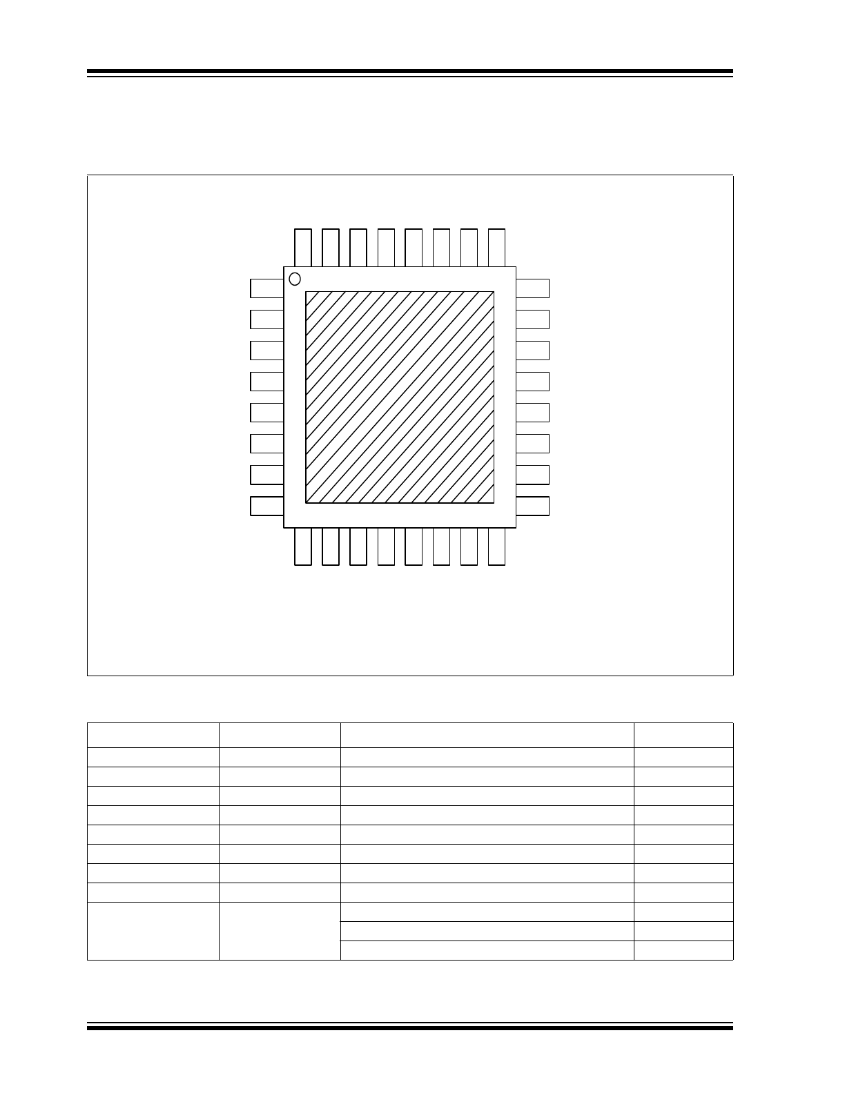
PIN DESCRIPTION
FIGURE 2-1:
CAP1114 PIN DIAGRAM (32-PIN QFN)
TABLE 2-1:
PIN DESCRIPTION FOR CAP1114
Pin Number
Pin Name
Pin Function
Pin Type
1
CS8
Capacitive Touch Sensor 8
AIO
2
CS9
Capacitive Touch Sensor 9
AIO
3
CS10
Capacitive Touch Sensor 10
AIO
4
CS11
Capacitive Touch Sensor 11
AIO
5
CS12
Capacitive Touch Sensor 12
AIO
6
CS13
Capacitive Touch Sensor 13
AIO
7
CS14
Capacitive Touch Sensor 14
AIO
8
VDD
Positive Power supply
Power
9
LED1 / GPIO1
LED1 - Open drain LED driver (default)
OD (5V)
GPI1 - GPIO 1 Input
DI (5V)
GPO1 - GPIO 1 push-pull output
DO
1
2
3
4
5
6
7
24
23
22
21
20
19
18
32
31
30
29
28
27
26
9
10
11
12
13
14
15
CS8
LE
D1 /
GPI
O
1
CS9
CS10
CS11
L
E
D
2
/ G
P
IO2
L
E
D
3
/ G
P
IO3
CS12
CS13
CS14
L
E
D
4
/ G
P
IO4
L
E
D
5
/
GP
IO5
L
E
D
6
/
GP
IO6
CS
6
CS
5
CS
4
CS
3
CS
2
L
E
D
7
/ G
P
IO7
LED10
LED9
L
E
D
8
/ G
P
IO8
SMCLK
ALERT
SMDATA
CS
7
VDD
LED11
8
16
17
25
GND
RESET
N/C
N/C
CS
1

2009-2017 Microchip Technology Inc.
DS00002444A-page 7
CAP1114
The pin types are described in
Table 2-2, "Pin Types"
. All pins labeled with (5V) are 5V tolerant.
10
LED2 / GPIO 2
LED2 - Open drain LED driver (default)
OD (5V)
GPI2 - GPIO 2 Input
DI (5V)
GPO2 - GPIO 2 push-pull output
DO
11
LED3 / GPIO3
LED3 - Open drain LED driver (default)
OD (5V)
GPI3 - GPIO 3 Input
DI (5V)
GPO3 - GPIO 3 push-pull output
DO
12
LED4 / GPIO4
LED4 - Open drain LED driver (default)
OD (5V)
GPI4 - GPIO 4 Input
DI (5V)
GPO4 - GPIO 4 push-pull output
DO
13
LED5 / GPIO5
LED5 - Open drain LED driver (default)
OD (5V)
GPI5 - GPIO 5 Input
DI (5V)
GPO5 - GPIO 5 push-pull output
DO
14
LED6 / GPIO6
LED6 - Open drain LED driver (default)
OD (5V)
GPI6 - GPIO 6 Input
DI (5V)
GPO6 - GPIO 6 push-pull output
DO
15
LED7 / GPIO7
LED7 - Open drain LED driver (default)
OD (5V)
GPI7 - GPIO 7 Input
DI (5V)
GPO7 - GPIO 7 push-pull output
DO
16
LED8 / GPIO8
LED8 - Open drain LED driver (default)
OD (5V)
GPI8 - GPIO 8 Input
DI (5V)
GPO8 - GPIO 8 push-pull output
DO
17
LED9
LED9 - Open drain LED driver
OD (5V)
18
LED10
LED10 - Open drain LED driver
OD (5V)
19
LED11
LED11 - Open drain LED driver
OD (5V)
20
ALERT
Active High Interrupt / Wake Up Input
DIO
21
SMDATA
Bi-directional SMBus data - requires a pull-up
resistor
DIOD (5V)
22
SMCLK
SMBus clock input - requires a pull-up resistor
DI (5V)
23
RESET
Soft reset for system - resets all registers to default
values
DI (5V)
24
N/C
Not Connected - connect to gnd
N/A
25
N/C
Not Connected - connect to gnd
N/A
26
CS1
Capacitive Touch Sensor 1
AIO
27
CS2
Capacitive Touch Sensor 2
AIO
28
CS3
Capacitive Touch Sensor 3
AIO
29
CS4
Capacitive Touch Sensor 4
AIO
30
CS5
Capacitive Touch Sensor 5
AIO
31
CS6
Capacitive Touch Sensor 6
AIO
32
CS7
Capacitive Touch Sensor 7
AIO
Bottom Plate
GND
Power Ground
Power
Note:
For all 5V tolerant pins that require a pull-up resistor, the voltage difference between VDD and the pull-up
voltage must never exceed 3.6V.
TABLE 2-1:
PIN DESCRIPTION FOR CAP1114 (CONTINUED)
Pin Number
Pin Name
Pin Function
Pin Type

CAP1114
DS00002444A-page 8
2009-2017 Microchip Technology Inc.
TABLE 2-2:
PIN TYPES
Pin Type
Description
Power
This pin is used to supply power or ground to the device.
DI
Digital Input - this pin is used as a digital input. This pin is 5V tolerant.
DIO
Digital Input Output - this pin is used as a digital input / output.
AIO
Analog Input / Output - this pin is used as an I/O for analog signals.
DIOD
Digital Input / Open Drain Output - this pin is used as an digital I/O. When it is used as an
output, It is open drain and requires a pull-up resistor. This pin is 5V tolerant.
OD
Open Drain Digital Output - this pin is used as a digital output. It is open drain and requires
a pull-up resistor. This pin is 5V tolerant.
DO
Push-pull Digital Output - this pin is used as a digital output and can sink and source current.
2009-2017 Microchip Technology Inc.
DS00002444A-page 9
CAP1114
3.0
ELECTRICAL SPECIFICATIONS
Note 3-1
For the 5V tolerant pins that have a pull-up resistor, the pull-up voltage must not exceed 3.6V when
the device is unpowered.
Note 3-2
The Package Power Dissipation specification assumes a thermal via design with the thermal landing
be soldered to the PCB ground plane with 0.3mm (12mil) diameter vias in a 4x4 matrix at 0.9mm
(35.4mil) pitch.
Note 3-3
Junction to Ambient (
JA
) is dependent on the design of the thermal vias. Without thermal vias and
a thermal landing, the
JA
is approximately 60°C/W including localized PCB temperature increase.
TABLE 3-1:
ABSOLUTE MAXIMUM RATINGS
Voltage on VDD pin
-0.3 to 4
V
Voltage on 5V tolerant pins (V
5VT_PIN
)
-0.3 to 5.5
V
Voltage on 5V tolerant pins (|V
5VT_PIN
- V
DD
|) (see
Note 3-1
)
0 to 3.6
V
Voltage on any other pin to GND
-0.3 to VDD + 0.3
V
Package Power Dissipation up to T
A
= 85°C (see
Note 3-2
)
1
W
Junction to Ambient (
JA
) (see
Note 3-3
)
48
°C/W
Operating Ambient Temperature Range
-40 to 125
°C
Storage Temperature Range
-55 to 150
°C
ESD Rating, All Pins, HBM
8000
V
Note:
Stresses above those listed could cause permanent damage to the device. This is a stress rating only and
functional operation of the device at any other condition above those indicated in the operation sections of
this specification is not implied.
TABLE 3-2:
ELECTRICAL SPECIFICATIONS
V
DD
= 3V to 3.6V, T
A
= -40°C to 125°C, all Typical values at T
A
= 27°C unless otherwise noted.
Characteristic
Symbol
MIN
TYP
MAX
Unit
Conditions
DC Power
Supply Voltage
V
DD
3.0
3.3
3.6
V
Supply Current
I
DD
0.55
1
mA
Average current
Capacitive Sensing Active,
LEDs enabled
I
SLEEP
200
250
uA
Sleep state active, 1 sensor
monitored; LED11 inactive
T
A
< 85°C
I
DSLEEP
4.5
10
uA
Deep Sleep, LED 11 inactive
T
A
< 40°C
Time to
Communications
t
COMM
15
20
ms
Time from power applied to
communications active
Time to First
Conversion
t
CONV
400
500
ms
Time from power applied to first
sensor sampled
Capacitive Touch Sensor
Base Capacitance
C
BASE
5
15
50
pF
Pad untouched
Detectable Capacitive
Shift
C
TOUCH
0.1
0.4
2
pF
Pad touched
Sample Time
t
TOUCH
2.5
ms
Update Time
t
TOUCH
35
ms
Recalibration Interval
t
CAL
8
s
Automatic Recalibration active, no
touch active, default settings

CAP1114
DS00002444A-page 10
2009-2017 Microchip Technology Inc.
LED / GPIO Drivers (LED / GPIO 1 - 8)
Duty Cycle
DUTY
LED
0
100
%
Programmable
Drive Frequency
f
LED
2
kHz
Sinking Current
I
SINK
24
mA
V
OL
= 0.4
Sourcing Current
I
SOURCE
24
mA
V
OH
= V
DD
- 0.4
Input High Voltage
V
IH
2.0
V
LED / GPIO configured as input
Input Low Voltage
V
IL
0.8
V
LED / GPIO configured as input
LED Drivers (LED 9 - LED 10)
Duty Cycle
DUTY
LED
0
100
%
Programmable
Drive Frequency
f
LED
2
kHz
Sinking Current
I
SINK
24
mA
Output Low Voltage
V
OL
0.4
V
I
SINK
= 24mA
LED11 Driver
Duty Cycle
DUTY
LED
0
100
%
Programmable
Drive Frequency
f
LED
2
kHz
Sinking Current
I
SINK
48
mA
Output Low Voltage
V
OL
0.4
V
I
SINK
= 48mA
I/O Pins - SMDATA, SMCLK, and ALERT Pins
Output Low Voltage
V
OL
0.4
V
I
SINK_IO
= 8mA
Output High Voltage
V
OH
V
DD
- 0.4
V
ALERT pin active high and
asserted
I
SOURCE_IO
= 8mA
Input High Voltage
V
IH
2.0
V
Input Low Voltage
V
IL
0.8
V
Leakage Current
I
LEAK
±5
uA
powered or unpowered
TA < 85°C
pull-up voltage < 3.6V
RESET Pin
Input High Voltage
V
IH
2.0
V
Input Low Voltage
V
IL
0.8
V
RESET Filter Time
t
RST_FILT
10
ms
RESET Pin release to
fully active operation
t
RST_ON
400
500
ms
SMBus Timing
Input Capacitance
C
IN
5
pF
Clock Frequency
f
SMB
10
400
kHz
Spike Suppression
t
SP
50
ns
Bus free time Start to
Stop
t
BUF
1.3
us
Setup Time: Start
t
SU:STA
0.6
us
Setup Time: Stop
t
SU:STP
0.6
us
Data Hold Time
t
HD:DAT
0.6
6
us
Data Setup Time
t
SU:DAT
0.6
72
us
Clock Low Period
t
LOW
1.3
us
Clock High Period
t
HIGH
0.6
us
TABLE 3-2:
ELECTRICAL SPECIFICATIONS (CONTINUED)
V
DD
= 3V to 3.6V, T
A
= -40°C to 125°C, all Typical values at T
A
= 27°C unless otherwise noted.
Characteristic
Symbol
MIN
TYP
MAX
Unit
Conditions