
Features
•
High Performance, Low Power AVR
®
8-bit Microcontroller
•
Advanced RISC Architecture
– 123 Powerful Instructions – Most Single Clock Cycle Execution
– 32 x 8 General Purpose Working Registers
– Fully Static Operation
•
Non-volatile Program and Data Memories
– 4K Bytes of In-System Programmable Program Memory Flash
– 64 Bytes of In-System Programmable EEPROM
– 256 Bytes of Internal SRAM
– Write/Erase Cycles: 10,000 Flash/ 100,000 EEPROM
– Data Retention: 20 years at 85
°C/ 100 years at 25°C
– Programming Lock for Software Security
•
Peripheral Features
– QTouch
®
Library Support for Capacitive Touch Sensing (8 Channels)
– Two 8-bit Timer/Counters with two PWM Channels, Each
– Programmable Watchdog Timer with Separate On-chip Oscillator
– On-chip Analog Comparator
– 10-bit ADC
• 4 Single-ended Channels
– Universal Serial Interface
– Boost Converter
•
Special Microcontroller Features
– debugWIRE On-chip Debug System
– In-System Programmable via SPI Port
– External and Internal Interrupt Sources
– Pin Change Interrupt on 16 Pins
– Low Power Idle, ADC Noise Reduction and Power-down Modes
– Enhanced Power-on Reset Circuit
– Programmable Brown-out Detection Circuit
– Internal Calibrated Oscillator
– Temperature Sensor On-chip
•
I/O and Packages
– Available in 20-pin SOIC and 20-pin QFN/MLF
– 16 Programmable I/O Lines
•
Operating Voltage:
– 0.7 – 1.8V (via On-chip Boost Converter)
– 1.8 – 5.5V (Boost Converter Bypassed)
•
Speed Grade
– Using On-chip Boost Converter
• 0 – 4 MHz
– External Power Supply
• 0 – 4 MHz @ 1.8 – 5.5V
• 0 – 8 MHz @ 2.7 – 5.5V
•
Low Power Consumption
– Active Mode, 1 MHz System Clock
• 400 µA @ 3V (Without Boost Converter)
– Power-down Mode
• 150 nA @ 3V (Without Boost Converter)
8-bit
Microcontroller
with 4K Bytes
In-System
Programmable
Flash and Boost
Converter
ATtiny43U
Summary
Rev. 8048CS–AVR–02/12
2
8048CS–AVR–02/12
ATtiny43U
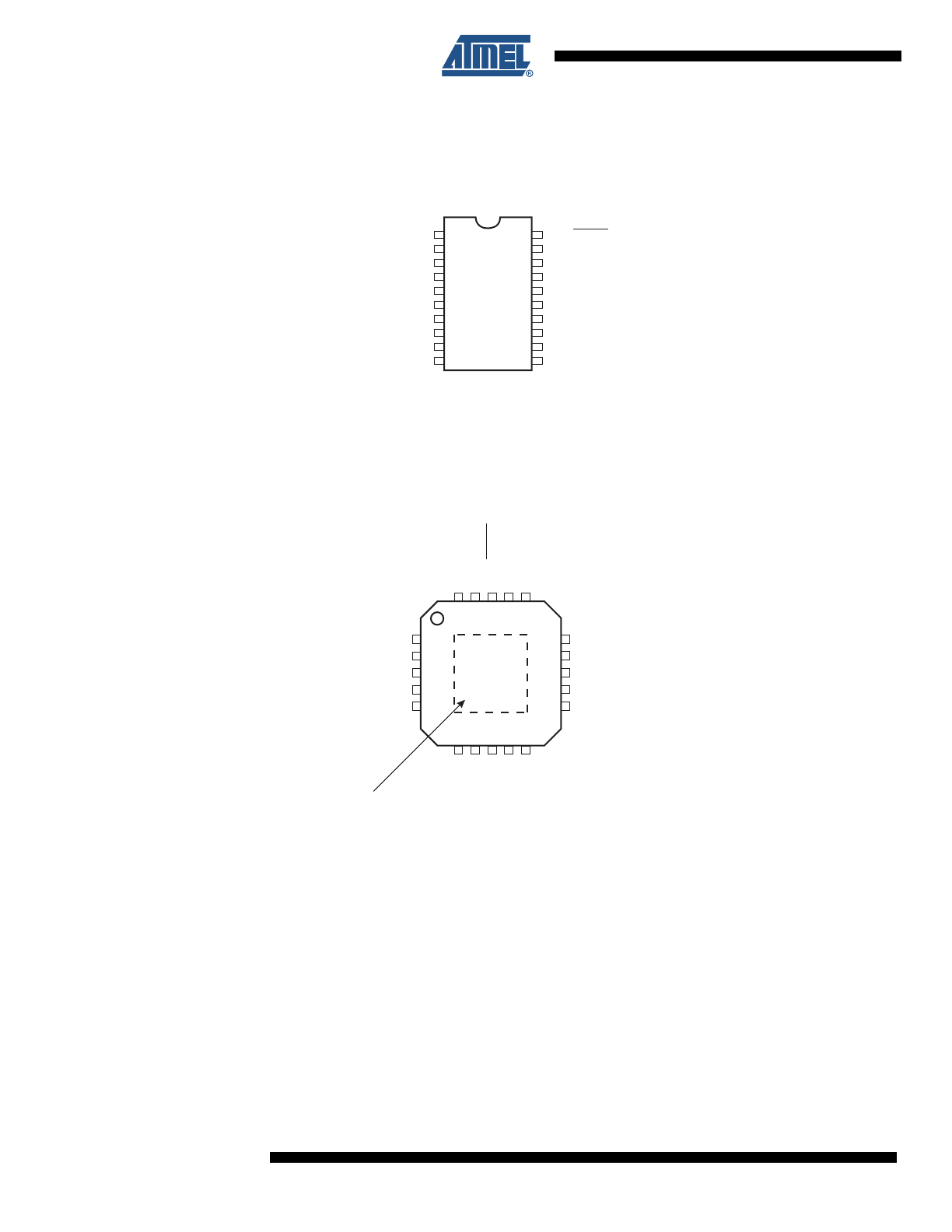
1.
Pin Configurations
Figure 1-1.
Pinout of ATtiny43U
1.1
Pin Descriptions
1.1.1
V
CC
Supply voltage.
1.1.2
GND
Ground.
1.1.3
Port A (PA7:PA0)
Port A is a 8-bit bi-directional I/O port with internal pull-up resistors (selected for each bit). The
Port A output buffers have symmetrical drive characteristics with both high sink and source
(T0/PCINT8) PB0
(OC0A/PCINT9) PB1
(OC0B/PCINT10) PB2
(T1/CLKO/PCINT11) PB3
(DI/OC1A/PCINT12) PB4
(DO/OC1B/PCINT13) PB5
(USCK/SCL/PCINT14) PB6
(INT0/PCINT15) PB7
VCC
GND
20
19
18
17
16
15
14
13
12
11
1
2
3
4
5
6
7
8
9
10
PA7 (RESET/dW/PCINT7)
PA6 (CLKI/PCINT6)
PA5 (AIN1/PCINT5)
PA4 (AIN0/PCINT4)
PA3 (ADC3/PCINT3)
PA2 (ADC2/PCINT2)
PA1 (ADC1/PCINT1)
PA0 (ADC0/PCINT0)
VBAT
LSW
QFN/MLF Top View
SOIC
NOTE: Bottom pad should
be Soldered to ground.
1
2
3
4
5
15
14
13
12
11
20
19
18
17
16
6
7
8
9
10
(OC0B/PCINT9) PB2
(T1/CLKO/PCINT11) PB
3
(DI/OC1A/PCINT12)
PB4
(DO/OC1B/PCINT13)
PB5
(USCK/SCL/PCINT14)
PB6
PA4 (AIN0/
PCINT4
)
PA3 (ADC3/
PCINT3
)
PA2 (ADC2/
PCINT2
)
PA1 (ADC1/
PCINT1
)
PA0 (ADC0/
PCINT0
)
(INT0/PCINT15)
PB7
VCC
GND
LSW
VBA
T
PB1
(OC0A/PCINT9)
PB0
(T0/PCINT8)
P
A7
(RESET/dW/PCINT7)
P
A6 (CLKI)
P
A5 (AIN1/PCINT5)

3
8048CS–AVR–02/12
ATtiny43U
capability except PA7 which has the RESET capability. To use pin PA7 as an I/O pin, instead of
RESET pin, program (‘0’) RSTDISBL fuse. As inputs, Port A pins that are externally pulled low
will source current if the pull-up resistors are activated. The Port A pins are tri-stated when a
reset condition becomes active, even if the clock is not running.
Port A has an alternate functions as analog inputs for the ADC, analog comparator, timer/coun-
ter, SPI and pin change interrupt as described in
“Alternate Port Functions” on page 69
.
1.1.4
RESET
Reset input. A low level on this pin for longer than the minimum pulse length will generate a
reset, even if the clock is not running. The minimum pulse length is given in
Table 20-4 on page
161
. Shorter pulses are not guaranteed to generate a reset.
1.1.5
Port B (PB7:PB0)
Port B is a 8-bit bi-directional I/O port with internal pull-up resistors (selected for each bit). The
Port B output buffers have symmetrical drive characteristics with both high sink and source
capability. As inputs, Port B pins that are externally pulled low will source current if the pull-up
resistors are activated. The Port B pins are tri-stated when a reset condition becomes active,
even if the clock is not running.
Port B also serves the functions of various special features as listed in
Section 11.3 “Alternate
Port Functions” on page 69
.
1.1.6
LSW
Boost converter external inductor connection. Connect to ground when boost converter is dis-
abled permanently.
1.1.7
V
BAT
Battery supply voltage. Connect to ground when boost converter is disabled permanently.
4
8048CS–AVR–02/12
ATtiny43U
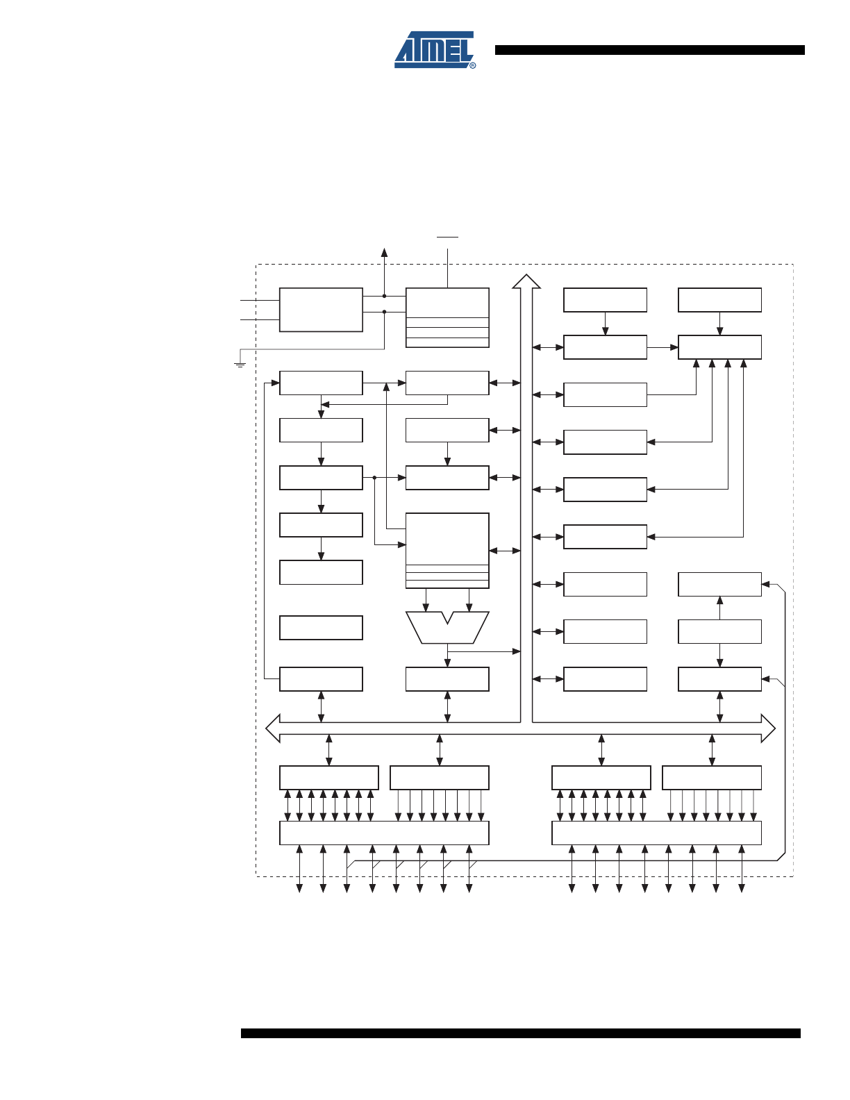
2.
Overview
The ATtiny43U is a low-power CMOS 8-bit microcontroller based on the AVR enhanced RISC
architecture. By executing powerful instructions in a single clock cycle, the ATtiny43U achieves
throughputs approaching 1 MIPS per MHz allowing the system designer to optimize power con-
sumption versus processing speed.
Figure 2-1.
Block Diagram
The AVR core combines a rich instruction set with 32 general purpose working registers. All the
32 registers are directly connected to the Arithmetic Logic Unit (ALU), allowing two independent
registers to be accessed in one single instruction executed in one clock cycle. The resulting
STACK
POINTER
SRAM
PROGRAM
COUNTER
BOOST
CONVERTER
PROGRAMMING
LOGIC
ISP
INTERFACE
INTERNAL
OSCILLATOR
WATCHDOG
TIMER
MCU CONTROL
REGISTER
MCU STATUS
REGISTER
TIMER/
COUNTER0
TIMER/
COUNTER1
CALIBRATED
OSCILLATOR
TIMING AND
CONTROL
INTERRUPT
UNIT
EEPROM
ANALOG
COMPARATOR
ADC
POWER
SUPERVISION
POR
BOD
RESET
ON-CHIP
DEBUG
VOLTAGE
REFERENCE
GENERAL
PURPOSE
REGISTERS
X
Y
Z
ALU
STATUS
REGISTER
PROGRAM
FLASH
INSTRUCTION
REGISTER
INSTRUCTION
DECODER
CONTROL
LINES
DATA REGISTER
PORT A
DIRECTION REG.
PORT A
DRIVERS
PORT A
V
CC
VBAT
LSW
RESET
DATA REGISTER
PORT B
DIRECTION REG.
PORT B
DRIVERS
PORT B
GND
USI
PA[7:0]
PB[7:0]

5
8048CS–AVR–02/12
ATtiny43U
architecture is more code efficient while achieving throughputs up to ten times faster than con-
ventional CISC microcontrollers.
The ATtiny43U provides the following features: 4K byte of In-System Programmable Flash, 64
bytes EEPROM, 256 bytes SRAM, 16 general purpose I/O lines, 32 general purpose working
registers, two 8-bit Timer/Counters with two PWM channels, Internal and External Interrupts, a
4-channel 10-bit ADC, Universal Serial Interface, a programmable Watchdog Timer with internal
Oscillator, internal calibrated oscillator, and three software selectable power saving modes. The
Idle mode stops the CPU while allowing the SRAM, Timer/Counter, ADC, Analog Comparator,
and Interrupt system to continue functioning. The Power-down mode saves the register con-
tents, disabling all chip functions until the next Interrupt or Hardware Reset. The ADC Noise
Reduction mode stops the CPU and all I/O modules except ADC, to minimize switching noise
during ADC conversions.
A special feature of ATtiny43U is the built-in boost voltage converter, which provides 3V supply
voltage from an external, low voltage.
The device is manufactured using Atmel’s high density non-volatile memory technology. The
On-chip ISP Flash allows the Program memory to be re-programmed In-System through an SPI
serial interface, by a conventional non-volatile memory programmer or by an On-chip boot code
running on the AVR core.
The ATtiny43U AVR is supported by a full suite of program and system development tools
including: C Compilers, Macro Assemblers, Program Debugger/Simulators, In-Circuit Emulators,
and Evaluation kits.

6
8048CS–AVR–02/12
ATtiny43U
3.
General Information
3.1
Resources
A comprehensive set of development tools, drivers and application notes, and datasheets are
available for download on http://www.atmel.com/avr.
3.2
Code Examples
This documentation contains simple code examples that briefly show how to use various parts of
the device. These code examples assume that the part specific header file is included before
compilation. Be aware that not all C compiler vendors include bit definitions in the header files
and interrupt handling in C is compiler dependent. Please confirm with the C compiler documen-
tation for more details.
For I/O Registers located in extended I/O map, “IN”, “OUT”, “SBIS”, “SBIC”, “CBI”, and “SBI”
instructions must be replaced with instructions that allow access to extended I/O. Typically
“LDS” and “STS” combined with “SBRS”, “SBRC”, “SBR”, and “CBR”.
3.3
Capacitive Touch Sensing
Atmel QTouch Library provides a simple to use solution for touch sensitive interfaces on Atmel
AVR microcontrollers. The QTouch Library includes support for QTouch
®
and QMatrix
®
acquisi-
tion methods.
Touch sensing is easily added to any application by linking the QTouch Library and using the
Application Programming Interface (API) of the library to define the touch channels and sensors.
The application then calls the API to retrieve channel information and determine the state of the
touch sensor.
The QTouch Library is free and can be downloaded from the Atmel website. For more informa-
tion and details of implementation, refer to the QTouch Library User Guide – also available from
the Atmel website.
3.4
Data Retention
Reliability Qualification results show that the projected data retention failure rate is much less
than 1 PPM over 20 years at 85°C or 100 years at 25°C.
7
8048CS–AVR–02/12
ATtiny43U
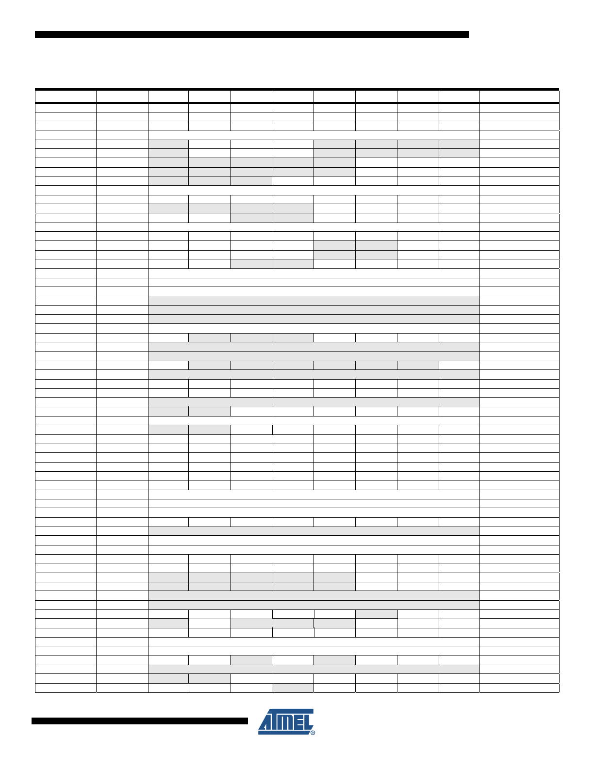
4.
Register Summary
Address
Name
Bit 7
Bit 6
Bit 5
Bit 4
Bit 3
Bit 2
Bit 1
Bit 0
Page
0x3F (0x5F)
SREG
I
T
H
S
V
N
Z
C
Page 9
0x3E (0x5E)
SPH
–
–
–
–
–
–
–
SP8
Page 12
0x3D (0x5D)
SPL
SP7
SP6
SP5
SP4
SP3
SP2
SP1
SP0
Page 12
0x3C (0x5C)
OCR0B
Timer/Counter0 – Output Compare Register B
Page 97
0x3B (0x5B)
GIMSK
–
INT0
PCIE1
PCIE0
–
–
–
–
Page 61
0x3A (0x5A)
GIFR
–
INTF0
PCIF1
PCIF0
–
–
–
–
Page 61
0x39 (0x59)
TIMSK0
–
–
–
–
–
OCIE0B
OCIE0A
TOIE0
Page 97
0x38 (0x58)
TIFR0
–
–
–
–
–
OCF0B
OCF0A
TOV0
Page 98
0x37 (0x57)
SPMCSR
–
–
–
CTPB
RFLB
PGWRT
PGERS
SPMEN
Page 139
0x36 (0x56)
OCR0A
Timer/Counter0 – Output Compare Register A
Page 97
0x35 (0x55)
MCUCR
BODS
PUD
SE
SM1
SM0
BODSE
ISC01
ISC00
Pages
33
,
60
,
79
0x34 (0x54)
MCUSR
–
–
–
–
WDRF
BORF
EXTRF
PORF
Page 55
0x33 (0x53)
TCCR0B
FOC0A
FOC0B
–
–
WGM02
CS02
CS01
CS00
Page 95
0x32 (0x52)
TCNT0
Timer/Counter0
Page 96
0x31 (0x51)
OSCCAL
CAL7
CAL6
CAL5
CAL4
CAL3
CAL2
CAL1
CAL0
Page 28
0x30 (0x50)
TCCR0A
COM0A1
COM0A0
COM0B1
COM0B0
–
WGM01
WGM00
Page 92
0x2F (0x4F)
TCCR1A
COM1A1
COM1A0
COM1B1
COM1B0
–
WGM11
WGM10
Page 92
0x2E (0x4E)
TCCR1B
FOC1A
FOC1B
–
–
WGM12
CS12
CS11
CS10
Page 95
0x2D (0x4D)
TCNT1
Timer/Counter1
Page 97
0x2C (0x4C)
OCR1A
Timer/Counter1 – Output Compare Register A
Page 97
0x2B (0x4B)
OCR1B
Timer/Counter1 – Output Compare Register B
Page 97
0x2A (0x4A)
Reserved
–
0x29 (0x49)
Reserved
–
0x28 (0x48)
Reserved
–
0x27 (0x47)
DWDR
DWDR[7:0]
Page 134
0x26 (0x46)
CLKPR
CLKPCE
–
–
–
CLKPS3
CLKPS2
CLKPS1
CLKPS0
Page 28
0x25 (0x45)
Reserved
–
0x24 (0x44)
Reserved
–
0x23 (0x43)
GTCCR
TSM
–
–
–
–
–
–
PSR10
Page 101
0x22 (0x42)
Reserved
–
0x21 (0x41)
WDTCSR
WDIF
WDIE
WDP3
WDCE
WDE
WDP2
WDP1
WDP0
Page 55
0x20 (0x40)
PCMSK1
PCINT15
PCINT14
PCINT13
PCINT12
PCINT11
PCINT10
PCINT9
PCINT8
Page 62
0x1F (0x3F)
Reserved
–
0x1E (0x3E)
EEAR
–
–
EEAR5
EEAR4
EEAR3
EEAR2
EEAR1
EEAR0
Page 20
0x1D (0x3D)
EEDR
EEPROM Data Register
Page 21
0x1C (0x3C)
EECR
–
–
EEPM1
EEPM0
EERIE
EEMPE
EEPE
EERE
Page 21
0x1B (0x3B)
PORTA
PORTA7
PORTA6
PORTA5
PORTA4
PORTA3
PORTA2
PORTA1
PORTA0
Page 79
0x1A (0x3A)
DDRA
DDA7
DDA6
DDA5
DDA4
DDA3
DDA2
DDA1
DDA0
Page 79
0x19 (0x39)
PINA
PINA7
PINA6
PINA5
PINA4
PINA3
PINA2
PINA1
PINA0
Page 79
0x18 (0x38)
PORTB
PORTB7
PORTB6
PORTB5
PORTB4
PORTB3
PORTB2
PORTB1
PORTB0
Page 79
0x17 (0x37)
DDRB
DDB7
DDB6
DDB5
DDB4
DDB3
DDB2
DDB1
DDB0
Page 79
0x16 (0x36)
PINB
PINB7
PINB6
PINB5
PINB4
PINB3
PINB2
PINB1
PINB0
Page 79
0x15 (0x35)
GPIOR2
General Purpose I/O Register 2
Page 22
0x14 (0x34)
GPIOR1
General Purpose I/O Register 1
Page 22
0x13 (0x33)
GPIOR0
General Purpose I/O Register 0
Page 22
0x12 (0x32)
PCMSK0
PCINT7
PCINT6
PCINT5
PCINT4
PCINT3
PCINT2
PCINT1
PCINT0
Page 62
0x11 (0x31)
Reserved
–
0x10 (0x30)
USIBR
USI Buffer Register
Page 113
0x0F (0x2F)
USIDR
USI Data Register
Page 112
0x0E (0x2E)
USISR
USISIF
USIOIF
USIPF
USIDC
USICNT3
USICNT2
USICNT1
USICNT0
Page 111
0x0D (0x2D)
USICR
USISIE
USIOIE
USIWM1
USIWM0
USICS1
USICS0
USICLK
USITC
Page 109
0x0C (0x2C)
TIMSK1
–
–
–
–
–
OCIE1B
OCIE1A
TOIE1
Page 98
0x0B (0x2B)
TIFR1
–
–
–
–
–
OCF1B
OCF1A
TOV1
Page 98
0x0A (0x2A)
Reserved
–
0x09 (0x29)
Reserved
–
0x08 (0x28)
ACSR
ACD
ACBG
ACO
ACI
ACIE
–
ACIS1
ACIS0
Page 115
0x07 (0x27)
ADMUX
–
REFS
–
–
–
MUX2
MUX1
MUX0
Page 128
0x06 (0x26)
ADCSRA
ADEN
ADSC
ADATE
ADIF
ADIE
ADPS2
ADPS1
ADPS0
Page 129
0x05 (0x25)
ADCH
ADC Data Register High Byte
Page 130
0x04 (0x24)
ADCL
ADC Data Register Low Byte
Page 130
0x03 (0x23)
ADCSRB
BS
ACME
–
ADLAR
–
ADTS2
ADTS1
ADTS0
Pages
48
, 115, 131
0x02 (0x22)
Reserved
–
0x01 (0x21)
DIDR0
AIN1D
AIN0D
ADC3D
ADC2D
ADC1D
ADC0D
Pages 116, 132
0x00 (0x20)
PRR
PRE2
PRE1
PRE0
–
PRTIM1
PRTIM0
PRUSI
PRADC
Page 34

8
8048CS–AVR–02/12
ATtiny43U
Note:
1. For compatibility with future devices, reserved bits should be written to zero if accessed. Reserved I/O memory addresses
should never be written.
2. I/O Registers within the address range 0x00 - 0x1F are directly bit-accessible using the SBI and CBI instructions. In these
registers, the value of single bits can be checked by using the SBIS and SBIC instructions.
3. Some of the Status Flags are cleared by writing a logical one to them. Note that, unlike most other AVRs, the CBI and SBI
instructions will only operation the specified bit, and can therefore be used on registers containing such Status Flags. The
CBI and SBI instructions work with registers 0x00 to 0x1F only.
9
8048CS–AVR–02/12
ATtiny43U
5.
Instruction Set Summary
Mnemonics
Operands
Description
Operation
Flags
#Clocks
ARITHMETIC AND LOGIC INSTRUCTIONS
ADD
Rd, Rr
Add two Registers
Rd
← Rd + Rr
Z,C,N,V,H
1
ADC
Rd, Rr
Add with Carry two Registers
Rd
← Rd + Rr + C
Z,C,N,V,H
1
ADIW
Rdl,K
Add Immediate to Word
Rdh:Rdl
← Rdh:Rdl + K
Z,C,N,V,S
2
SUB
Rd, Rr
Subtract two Registers
Rd
← Rd - Rr
Z,C,N,V,H
1
SUBI
Rd, K
Subtract Constant from Register
Rd
← Rd - K
Z,C,N,V,H
1
SBC
Rd, Rr
Subtract with Carry two Registers
Rd
← Rd - Rr - C
Z,C,N,V,H
1
SBCI
Rd, K
Subtract with Carry Constant from Reg.
Rd
← Rd - K - C
Z,C,N,V,H
1
SBIW
Rdl,K
Subtract Immediate from Word
Rdh:Rdl
← Rdh:Rdl - K
Z,C,N,V,S
2
AND
Rd, Rr
Logical AND Registers
Rd
← Rd • Rr
Z,N,V
1
ANDI
Rd, K
Logical AND Register and Constant
Rd
← Rd • K
Z,N,V
1
OR
Rd, Rr
Logical OR Registers
Rd
← Rd v Rr
Z,N,V
1
ORI
Rd, K
Logical OR Register and Constant
Rd
← Rd v K
Z,N,V
1
EOR
Rd, Rr
Exclusive OR Registers
Rd
← Rd ⊕ Rr
Z,N,V
1
COM
Rd
One’s Complement
Rd
← 0xFF − Rd
Z,C,N,V
1
NEG
Rd
Two’s Complement
Rd
← 0x00 − Rd
Z,C,N,V,H
1
SBR
Rd,K
Set Bit(s) in Register
Rd
← Rd v K
Z,N,V
1
CBR
Rd,K
Clear Bit(s) in Register
Rd
← Rd • (0xFF - K)
Z,N,V
1
INC
Rd
Increment
Rd
← Rd + 1
Z,N,V
1
DEC
Rd
Decrement
Rd
← Rd − 1
Z,N,V
1
TST
Rd
Test for Zero or Minus
Rd
← Rd • Rd
Z,N,V
1
CLR
Rd
Clear Register
Rd
← Rd ⊕ Rd
Z,N,V
1
SER
Rd
Set Register
Rd
← 0xFF
None
1
BRANCH INSTRUCTIONS
RJMP
k
Relative Jump
PC
← PC + k + 1
None
2
IJMP
Indirect Jump to (Z)
PC
← Z
None
2
RCALL
k
Relative Subroutine Call
PC
← PC + k + 1
None
3
ICALL
Indirect Call to (Z)
PC
← Z
None
3
RET
Subroutine Return
PC
← STACK
None
4
RETI
Interrupt Return
PC
← STACK
I
4
CPSE
Rd,Rr
Compare, Skip if Equal
if (Rd = Rr) PC
← PC + 2 or 3
None
1/2/3
CP
Rd,Rr
Compare
Rd
− Rr
Z, N,V,C,H
1
CPC
Rd,Rr
Compare with Carry
Rd
− Rr − C
Z, N,V,C,H
1
CPI
Rd,K
Compare Register with Immediate
Rd
− K
Z, N,V,C,H
1
SBRC
Rr, b
Skip if Bit in Register Cleared
if (Rr(b)=0) PC
← PC + 2 or 3
None
1/2/3
SBRS
Rr, b
Skip if Bit in Register is Set
if (Rr(b)=1) PC
← PC + 2 or 3
None
1/2/3
SBIC
P, b
Skip if Bit in I/O Register Cleared
if (P(b)=0) PC
← PC + 2 or 3
None
1/2/3
SBIS
P, b
Skip if Bit in I/O Register is Set
if (P(b)=1) PC
← PC + 2 or 3
None
1/2/3
BRBS
s, k
Branch if Status Flag Set
if (SREG(s) = 1) then PC
←PC+k + 1
None
1/2
BRBC
s, k
Branch if Status Flag Cleared
if (SREG(s) = 0) then PC
←PC+k + 1
None
1/2
BREQ
k
Branch if Equal
if (Z = 1) then PC
← PC + k + 1
None
1/2
BRNE
k
Branch if Not Equal
if (Z = 0) then PC
← PC + k + 1
None
1/2
BRCS
k
Branch if Carry Set
if (C = 1) then PC
← PC + k + 1
None
1/2
BRCC
k
Branch if Carry Cleared
if (C = 0) then PC
← PC + k + 1
None
1/2
BRSH
k
Branch if Same or Higher
if (C = 0) then PC
← PC + k + 1
None
1/2
BRLO
k
Branch if Lower
if (C = 1) then PC
← PC + k + 1
None
1/2
BRMI
k
Branch if Minus
if (N = 1) then PC
← PC + k + 1
None
1/2
BRPL
k
Branch if Plus
if (N = 0) then PC
← PC + k + 1
None
1/2
BRGE
k
Branch if Greater or Equal, Signed
if (N
⊕ V= 0) then PC ← PC + k + 1
None
1/2
BRLT
k
Branch if Less Than Zero, Signed
if (N
⊕ V= 1) then PC ← PC + k + 1
None
1/2
BRHS
k
Branch if Half Carry Flag Set
if (H = 1) then PC
← PC + k + 1
None
1/2
BRHC
k
Branch if Half Carry Flag Cleared
if (H = 0) then PC
← PC + k + 1
None
1/2
BRTS
k
Branch if T Flag Set
if (T = 1) then PC
← PC + k + 1
None
1/2
BRTC
k
Branch if T Flag Cleared
if (T = 0) then PC
← PC + k + 1
None
1/2
BRVS
k
Branch if Overflow Flag is Set
if (V = 1) then PC
← PC + k + 1
None
1/2
BRVC
k
Branch if Overflow Flag is Cleared
if (V = 0) then PC
← PC + k + 1
None
1/2
BRIE
k
Branch if Interrupt Enabled
if ( I = 1) then PC
← PC + k + 1
None
1/2
BRID
k
Branch if Interrupt Disabled
if ( I = 0) then PC
← PC + k + 1
None
1/2
BIT AND BIT-TEST INSTRUCTIONS
SBI
P,b
Set Bit in I/O Register
I/O(P,b)
← 1
None
2
CBI
P,b
Clear Bit in I/O Register
I/O(P,b)
← 0
None
2
LSL
Rd
Logical Shift Left
Rd(n+1)
← Rd(n), Rd(0) ← 0
Z,C,N,V
1
LSR
Rd
Logical Shift Right
Rd(n)
← Rd(n+1), Rd(7) ← 0
Z,C,N,V
1
ROL
Rd
Rotate Left Through Carry
Rd(0)
←C,Rd(n+1)← Rd(n),C←Rd(7)
Z,C,N,V
1
10
8048CS–AVR–02/12
ATtiny43U
ROR
Rd
Rotate Right Through Carry
Rd(7)
←C,Rd(n)← Rd(n+1),C←Rd(0)
Z,C,N,V
1
ASR
Rd
Arithmetic Shift Right
Rd(n)
← Rd(n+1), n=0..6
Z,C,N,V
1
SWAP
Rd
Swap Nibbles
Rd(3..0)
←Rd(7..4),Rd(7..4)←Rd(3..0)
None
1
BSET
s
Flag Set
SREG(s)
← 1
SREG(s)
1
BCLR
s
Flag Clear
SREG(s)
← 0
SREG(s)
1
BST
Rr, b
Bit Store from Register to T
T
← Rr(b)
T
1
BLD
Rd, b
Bit load from T to Register
Rd(b)
← T
None
1
SEC
Set Carry
C
← 1
C
1
CLC
Clear Carry
C
← 0
C
1
SEN
Set Negative Flag
N
← 1
N
1
CLN
Clear Negative Flag
N
← 0
N
1
SEZ
Set Zero Flag
Z
← 1
Z
1
CLZ
Clear Zero Flag
Z
← 0
Z
1
SEI
Global Interrupt Enable
I
← 1
I
1
CLI
Global Interrupt Disable
I
← 0
I
1
SES
Set Signed Test Flag
S
← 1
S
1
CLS
Clear Signed Test Flag
S
← 0
S
1
SEV
Set Twos Complement Overflow.
V
← 1
V
1
CLV
Clear Twos Complement Overflow
V
← 0
V
1
SET
Set T in SREG
T
← 1
T
1
CLT
Clear T in SREG
T
← 0
T
1
SEH
Set Half Carry Flag in SREG
H
← 1
H
1
CLH
Clear Half Carry Flag in SREG
H
← 0
H
1
DATA TRANSFER INSTRUCTIONS
MOV
Rd, Rr
Move Between Registers
Rd
← Rr
None
1
MOVW
Rd, Rr
Copy Register Word
Rd+1:Rd
← Rr+1:Rr
None
1
LDI
Rd, K
Load Immediate
Rd
← K
None
1
LD
Rd, X
Load Indirect
Rd
← (X)
None
2
LD
Rd, X+
Load Indirect and Post-Inc.
Rd
← (X), X ← X + 1
None
2
LD
Rd, - X
Load Indirect and Pre-Dec.
X
← X - 1, Rd ← (X)
None
2
LD
Rd, Y
Load Indirect
Rd
← (Y)
None
2
LD
Rd, Y+
Load Indirect and Post-Inc.
Rd
← (Y), Y ← Y + 1
None
2
LD
Rd, - Y
Load Indirect and Pre-Dec.
Y
← Y - 1, Rd ← (Y)
None
2
LDD
Rd,Y+q
Load Indirect with Displacement
Rd
← (Y + q)
None
2
LD
Rd, Z
Load Indirect
Rd
← (Z)
None
2
LD
Rd, Z+
Load Indirect and Post-Inc.
Rd
← (Z), Z ← Z+1
None
2
LD
Rd, -Z
Load Indirect and Pre-Dec.
Z
← Z - 1, Rd ← (Z)
None
2
LDD
Rd, Z+q
Load Indirect with Displacement
Rd
← (Z + q)
None
2
LDS
Rd, k
Load Direct from SRAM
Rd
← (k)
None
2
ST
X, Rr
Store Indirect
(X)
← Rr
None
2
ST
X+, Rr
Store Indirect and Post-Inc.
(X)
← Rr, X ← X + 1
None
2
ST
- X, Rr
Store Indirect and Pre-Dec.
X
← X - 1, (X) ← Rr
None
2
ST
Y, Rr
Store Indirect
(Y)
← Rr
None
2
ST
Y+, Rr
Store Indirect and Post-Inc.
(Y)
← Rr, Y ← Y + 1
None
2
ST
- Y, Rr
Store Indirect and Pre-Dec.
Y
← Y - 1, (Y) ← Rr
None
2
STD
Y+q,Rr
Store Indirect with Displacement
(Y + q)
← Rr
None
2
ST
Z, Rr
Store Indirect
(Z)
← Rr
None
2
ST
Z+, Rr
Store Indirect and Post-Inc.
(Z)
← Rr, Z ← Z + 1
None
2
ST
-Z, Rr
Store Indirect and Pre-Dec.
Z
← Z - 1, (Z) ← Rr
None
2
STD
Z+q,Rr
Store Indirect with Displacement
(Z + q)
← Rr
None
2
STS
k, Rr
Store Direct to SRAM
(k)
← Rr
None
2
LPM
Load Program Memory
R0
← (Z)
None
3
LPM
Rd, Z
Load Program Memory
Rd
← (Z)
None
3
LPM
Rd, Z+
Load Program Memory and Post-Inc
Rd
← (Z), Z ← Z+1
None
3
SPM
Store Program Memory
(z)
← R1:R0
None
IN
Rd, P
In Port
Rd
← P
None
1
OUT
P, Rr
Out Port
P
← Rr
None
1
PUSH
Rr
Push Register on Stack
STACK
← Rr
None
2
POP
Rd
Pop Register from Stack
Rd
← STACK
None
2
MCU CONTROL INSTRUCTIONS
NOP
No Operation
None
1
SLEEP
Sleep
(see specific descr. for Sleep function)
None
1
WDR
Watchdog Reset
(see specific descr. for WDR/Timer)
None
1
BREAK
Break
For On-chip Debug Only
None
N/A
Mnemonics
Operands
Description
Operation
Flags
#Clocks