
2016 Microchip Technology Inc.
DS20005661A-page 1
MIC5255
Features
• Input Voltage Range: 2.7V to 6.0V
• Thin SOT Package: 1 mm Height SOT-23-5
• Ultra-Low Output Noise: 30 µV
RMS
• Stability with Ceramic Output Capacitors
• Ultra-Low Dropout: 135 mV @ 150 mA
• High output accuracy:
- 1.0% Initial Accuracy
- 2.0% Over Temperature
• Low Quiescent Current: 90 µA
• Tight Load and Line Regulation
• TTL-Logic-Controlled Enable Input
• “Zero” Off-Mode Current
• Thermal Shutdown and Current-Limit Protection
Applications
• Cellular Telephones and Pagers
• Cellular Accessories
• Battery-Powered Equipment
• Laptop. Notebook, and Palmtop Computers
• Consumer/Personal Electronics
General Description
The MIC5255 is an efficient, precise CMOS voltage
regulator optimized for ultra-low-noise applications. It
offers 1% initial accuracy, extremely-low dropout
voltage (135 mV at 150 mA) and low ground current
(typically 117 µA at full load). The MIC5255 provides a
very low noise output, ideal for RF applications where
a clean voltage source is required. A noise bypass pin
is also available for further reduction of output noise.
Designed specifically for handheld and battery
powered devices, the MIC5255 provides a
TTL-logic-compatible enable pin. When disabled,
power consumption drops nearly to zero.
The MIC5255 also works with low-ESR ceramic
capacitors, reducing the amount of board space
necessary for power applications, critical in handheld
wireless devices.
Key features include current limit, thermal shutdown,
faster transient response, and an active clamp to speed
up device turn-off. Available in the 6-pin 2 mm × 2 mm
VDFN package, the SOT-23-5 package and the Thin
SOT-23-5, which offers the same footprint as the
standard SOT-23-5, but is only 1 mm tall. The MIC5255
offers a range of output voltages.
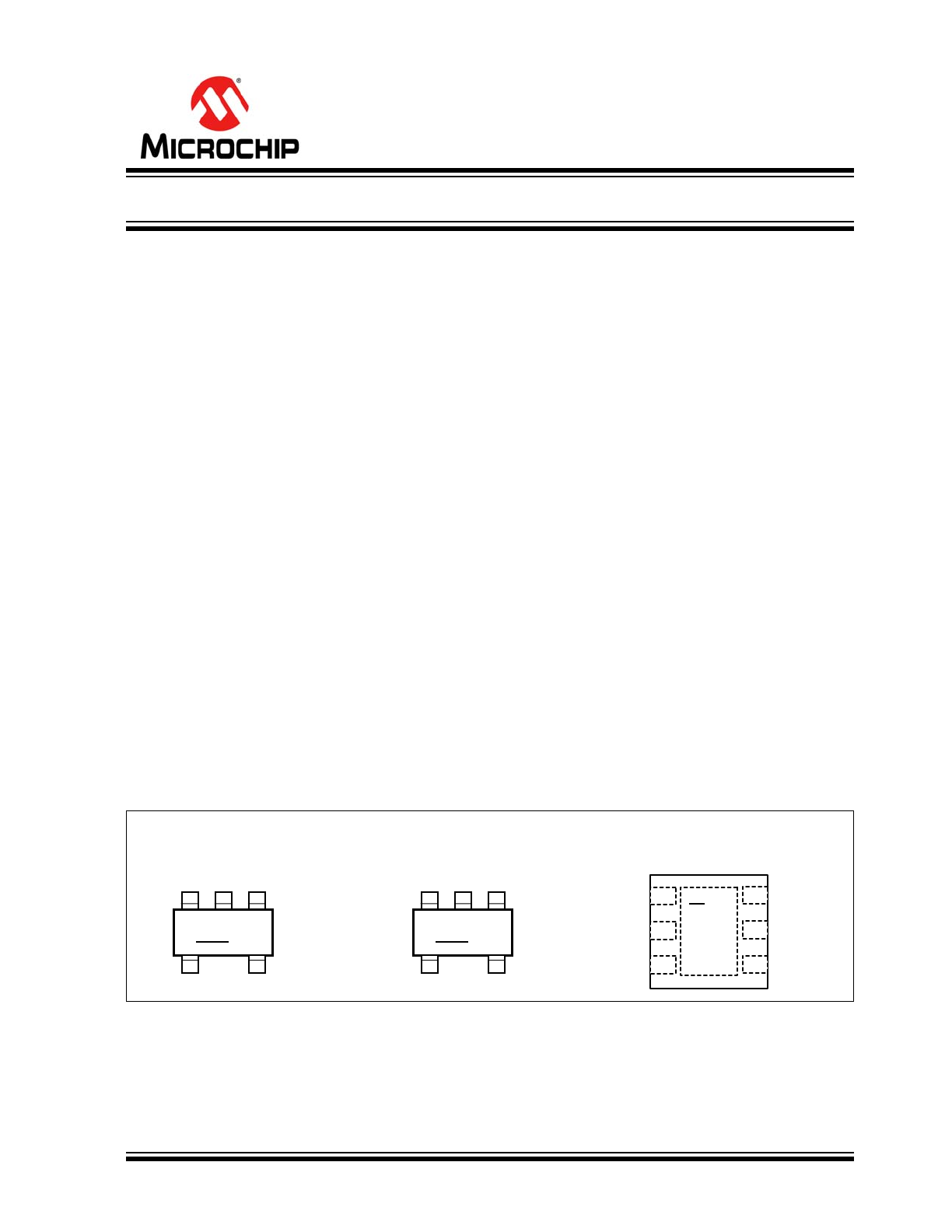
Package Types
MIC5255-x.xYM5
5-Pin SOT-23 (M5)
(Top View)
MIC5255-x.xYD5
5-Pin TSOT23 (D5)
(Top View)
IN
O U T
B Y P
E N
K W x x
1
3
2
GND
4
5
IN
O U T
B Y P
E N
N W x x
1
3
2
GND
4
5
MIC5255-x.xYML
6-Pin VDFN (ML)
(Top View)
1
EN
GND
IN
6
BYP
NC
OUT
5
4
2
3
W x x
150 mA Low Noise µCap CMOS LDO
MIC5255
DS20005661A-page 2
2016 Microchip Technology Inc.
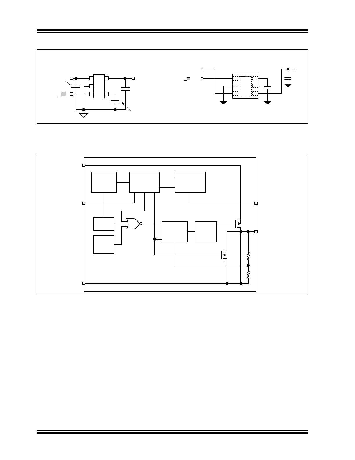
Typical Application Schematic
Block Diagram
MIC5255-
X
.
X
5-P
IN
SOT-23
MIC5255-
X
.
X
6-P
IN
2
X
2 VDFN
U
LTRA
-L
OW
-N
OISE
R
EGULATOR
A
PPLICATION
C
OUT
= 1.0μF
C
IN
= 1.0μF
Ceramic
Ceramic
1
5
2
3
4
C
BYP
= 0.01μF
Enable
Shutdown
EN
V
OUT
MIC5255-x.x_M5
EN (pin 3) may be
connected directly
to IN (pin 1).
V
IN
1
EN
ENABLE
SHUTDOWN
V
IN
6
C
BYP
(optional)
MIC5255-x.xYML
C
OUT
5
4
2
3
V
OUT
Reference
Voltage
Startup/
Shutdown
Control
E N
Q
uickstart/
Noise
Cancellation
Under-
voltage
Lockout
Thermal
Sensor
IN
F A U LT
Error
Amplifier
Current
Amplifier
GND
B Y P
OU T
A CTIV E S H U TDO W N

2016 Microchip Technology Inc.
DS20005661A-page 3
MIC5255
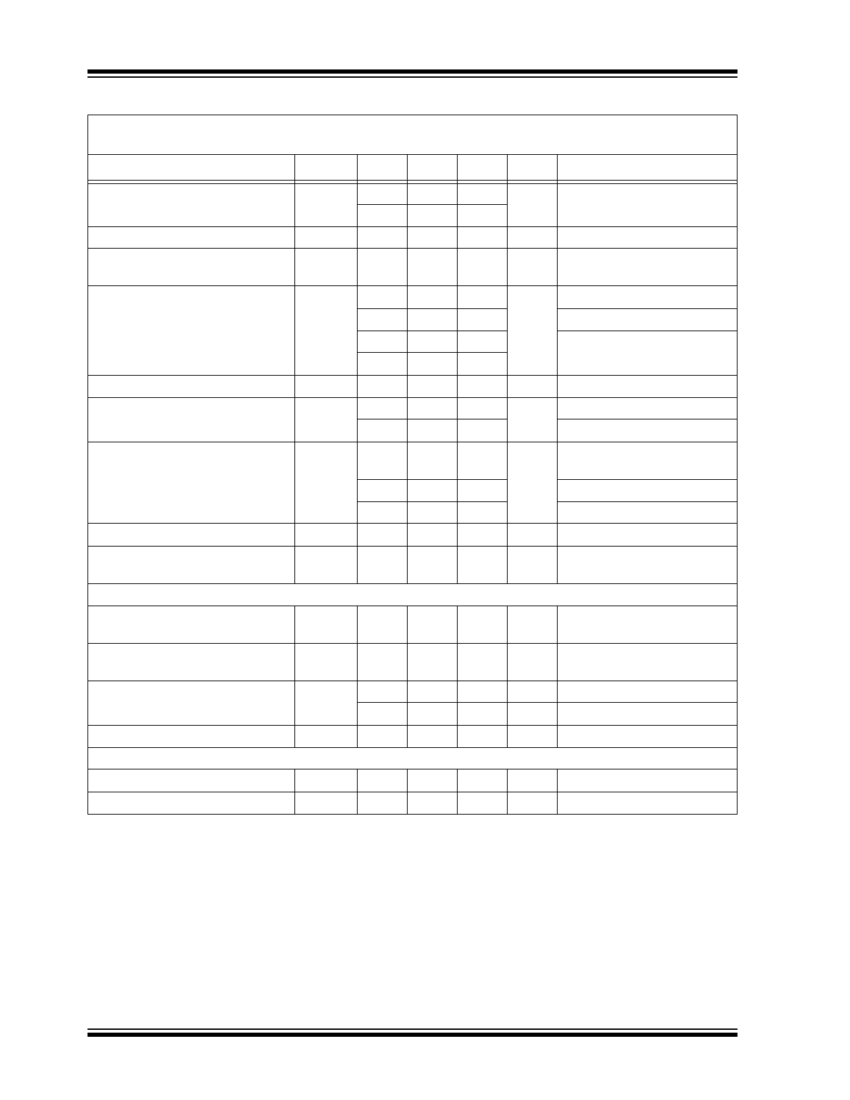
1.0
ELECTRICAL CHARACTERISTICS
Absolute Maximum Ratings †
Supply Voltage (V
IN
) ......................................................................................................................................... 0V to +7V
Enable Voltage (V
EN
) ........................................................................................................................................ 0V to +7V
Power Dissipation (P
D
,
Note 1
).............................................................................................................. Internally Limited
ESD Rating (
Note 2
) .................................................................................................................................................. 2 kV
Operating Ratings ‡
Supply Voltage (V
IN
) .................................................................................................................................... +2.7V to +6V
Enable Voltage (V
EN
) ..........................................................................................................................................0V to V
IN
† Notice: Stresses above those listed under “Absolute Maximum Ratings” may cause permanent damage to the device.
This is a stress rating only and functional operation of the device at those or any other conditions above those indicated
in the operational sections of this specification is not intended. Exposure to maximum rating conditions for extended
periods may affect device reliability.
‡ Notice: The device is not guaranteed to function outside its operating ratings.
Note 1: The maximum allowable power dissipation of any T
A
(ambient temperature) is P
D(max)
= (T
J(max)
– T
A
) / θ
JA
.
Exceeding the maximum allowable power dissipation will result in excessive die temperature, and the reg-
ulator will go into thermal shutdown. The θ
JA
of the MIC5255-x.xYM5 (all versions) is 235°C/W on a PC
board. See the
Thermal Considerations
section for further details.
2: Devices are ESD sensitive. Handling precautions recommended. Human body model, 1.5 kΩ in series with
100 pF.
MIC5255
DS20005661A-page 4
2016 Microchip Technology Inc.
TABLE 1-1:
ELECTRICAL CHARACTERISTICS
Electrical Characteristics: V
IN
= V
OUT
+ 1V, V
EN
= V
IN
; I
OUT
= 100 µA; T
J
= 25°C, bold values indicate –40°C ≤ T
J
≤ +125°C; unless noted. (
Note 1
).
Parameters
Sym.
Min.
Typ.
Max.
Units
Conditions
Output Voltage Accuracy
V
O
–1
—
1
%
I
OUT
= 100 µA
–2
—
2
Line Regulation
∆V
LNR
—
0.02
0.05
%/V
V
IN
= V
OUT
+ 1V to 6V
Load Regulation
∆V
LDR
—
1.5
2.5
%
I
OUT
= 0.1 mA to 150 mA;
Note 2
Dropout Voltage,
Note 3
V
IN
–
V
OUT
—
0.1
5
mV
I
OUT
= 100 µA
—
90
150
I
OUT
= 100 mA
—
135
200
I
OUT
= 150 mA
—
—
250
Quiescent Current
I
Q
—
0.2
5
µA
V
EN
≤ 0.4V (shutdown)
Ground Pin Current,
Note 4
I
GND
—
90
150
µA
I
OUT
= 0 mA
—
117
—
I
OUT
= 150 mA
Ripple Rejection
PSRR
—
60
—
dB
f = 10 Hz, C
OUT
= 1.0 µF,
C
BYP
= 0.01 µF
—
60
—
f = 100 Hz, V
IN
= V
OUT
+1V
—
50
—
f = 10 kHz, V
IN
= V
OUT
+1V
Current Limit
I
LIM
160
425
—
mA
V
OUT
= 0V
Output Voltage Noise
e
n
—
30
—
µV
RMS
C
OUT
= 1.0 µF, C
BYP
= 0.01 µF,
f = 10 Hz to 100 kHz
Enable Input
Enable Input Logic-Low Voltage
V
IL
—
—
0.4
V
V
IN
= 2.7V to 5.5V,
regulator shutdown
Enable Input Logic-High Voltage
V
IH
1.6
—
—
V
V
IN
= 2.7V to 5.5V,
regulator enabled
Enable Input Current
I
EN
—
0.01
—
µA
V
IL
≤ 0.4V, regulator shutdown
—
0.01
—
µA
V
IH
≥ 1.6V, regulator enabled
Shutdown Resistance Discharge
—
—
500
—
Ω
—
Thermal Protection
Thermal Shutdown Temperature
—
—
150
—
°C
—
Thermal Shutdown Hysteresis
—
—
10
—
°C
—
Note 1: Specification for packaged product only.
2: Regulation is measured at constant junction temperature using low duty cycle pulse testing. Parts are
tested for load regulation in the load range from 1.0 mA to 150 mA. Changes in output voltage due to
heating effects are covered by the thermal regulation specification.
3: Dropout voltage is defined as the input to output differential at which the output voltage drops 2% below its
nominal value measured at 1V differential. For outputs below 2.7V, dropout voltage is the input-to-output
voltage differential with the minimum input voltage 2.7V. Minimum input operating voltage is 2.7V.
4: Ground pin current is the regulator quiescent current. The total current drawn from the supply is the sum of
the load current plus the ground pin current.
2016 Microchip Technology Inc.
DS20005661A-page 5
MIC5255
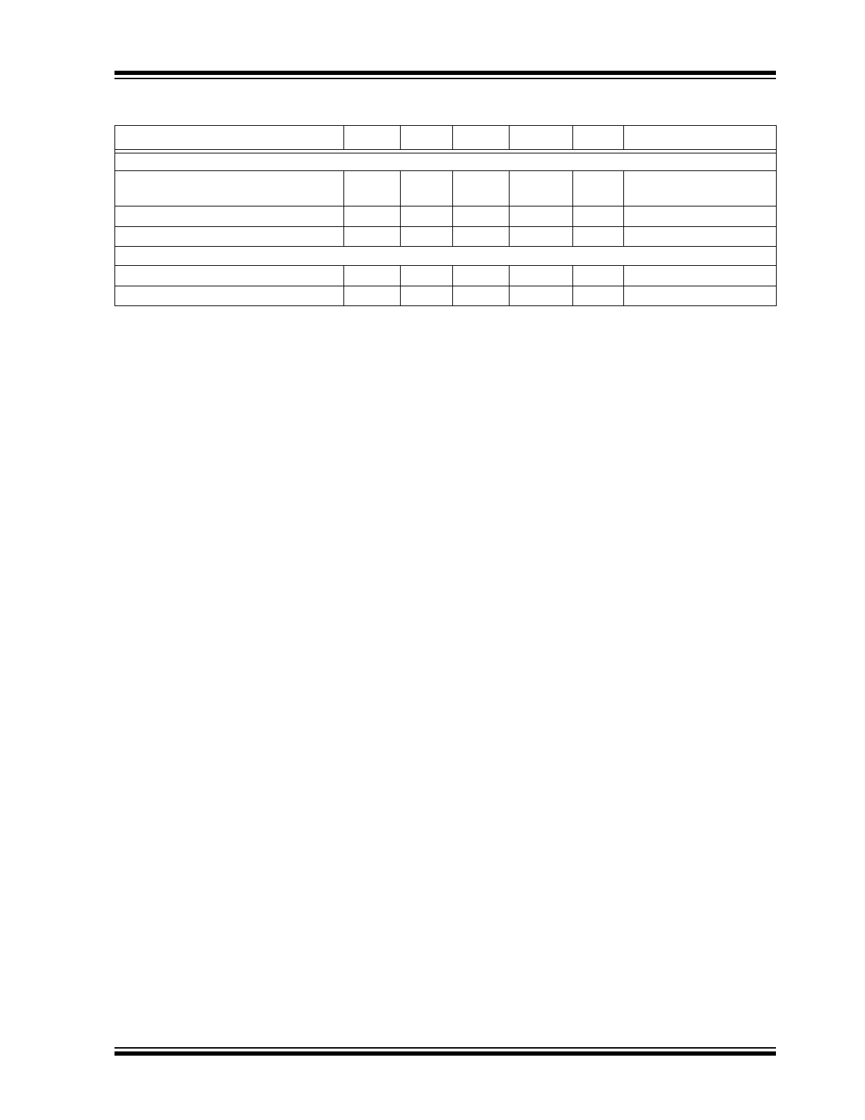
TEMPERATURE SPECIFICATIONS
Parameters
Sym.
Min.
Typ.
Max.
Units
Conditions
Temperature Ranges
Junction Operating Temperature
Range
T
J
–40
—
+125
°C
Note 1
Storage Temperature
T
S
–60
—
+150
°C
—
Lead Temperature
—
—
—
+260
°C
Soldering, 5s
Package Thermal Resistances
Thermal Resistance, SOT-23-5
JA
—
235
—
°C/W
—
Thermal Resistance, 2x2 VDFN-6
JA
—
90
—
°C/W
—
Note 1: The maximum allowable power dissipation is a function of ambient temperature, the maximum allowable
junction temperature and the thermal resistance from junction to air (i.e., T
A
, T
J
,
JA
). Exceeding the
maximum allowable power dissipation will cause the device operating junction temperature to exceed the
maximum +125°C rating. Sustained junction temperatures above +125°C can impact the device reliability.
MIC5255
DS20005661A-page 6
2016 Microchip Technology Inc.
2.0
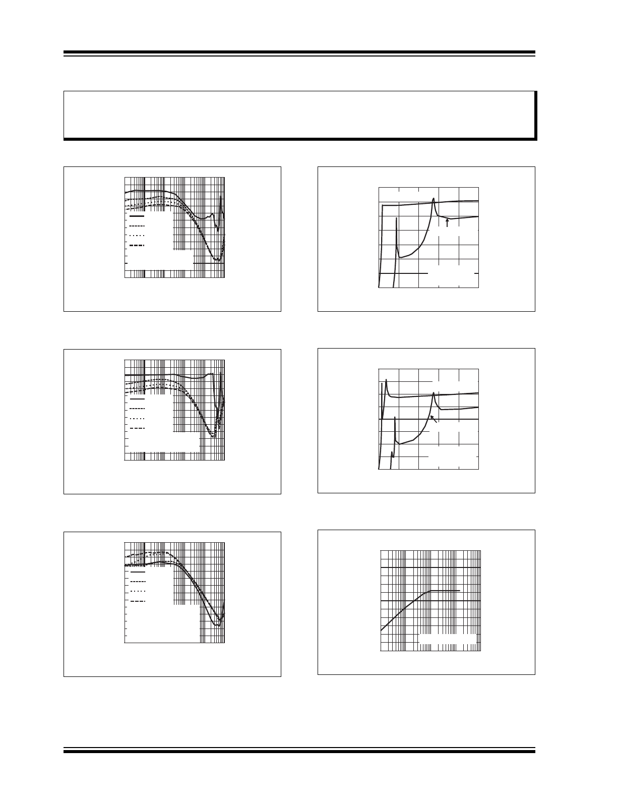
TYPICAL PERFORMANCE CURVES
FIGURE 2-1:
Power Supply Rejection
Ratio.
FIGURE 2-2:
Power Supply Rejection
Ratio.
FIGURE 2-3:
Power Supply Rejection
Ratio.
FIGURE 2-4:
PSRR vs. Voltage Drop.
FIGURE 2-5:
PSRR vs. Voltage Drop.
FIGURE 2-6:
Ground Pin Current.
Note:
The graphs and tables provided following this note are a statistical summary based on a limited number of
samples and are provided for informational purposes only. The performance characteristics listed herein
are not tested or guaranteed. In some graphs or tables, the data presented may be outside the specified
operating range (e.g., outside specified power supply range) and therefore outside the warranted range.
0
10
20
30
40
50
60
70
0
1
0
0
1
0
0
0
1
0
0
0
0
1
0
0
0
0
0
1
0
0
0
0
0
0
1
)
B
d(
R
R
S
P
FREQUENCY (Hz)
100μA*
50mA*
100mA*
150mA*
*I
LOAD
C
OUT
= 1μF Ceramic
0
10
20
30
40
50
60
70
0
1
0
0
1
0
0
0
1
0
0
0
0
1
0
0
0
0
0
1
0
0
0
0
0
0
1
)
B
d(
R
R
S
P
FREQUENCY (Hz)
100μA*
50mA*
100mA*
150mA*
* I
LOAD
C
OUT
= 4.7μF Ceramic
0
10
20
30
40
50
60
70
0
1
0
0
1
0
0
0
1
0
0
0
0
1
0
0
0
0
0
1
0
0
0
0
0
0
1
)
B
d(
R
R
S
P
FREQUENCY (Hz)
0μF*
0.01μF*
0.1μF*
1.0μF*
* C
BYP
I
LOAD
= 50mA
V
IN
= V
OUT
+ 0.5V
C
OUT
= 1μF Ceramic
0
10
20
30
40
50
60
70
0
200
400
600
800
1000
)
B
d(
R
R
S
P
VOLTAGE DROP (mV)
I
LOAD
= 100μA
I
LOAD
= 150mA
C
OUT
= 1μF
C
BYP
= 0
0
10
20
30
40
50
60
70
80
0
200
400
600
800
1000
)
B
d(
R
R
S
P
VOLTAGE DROP (mV)
I
LOAD
= 100μA
I
LOAD
= 150mA
C
OUT
= 1μF
C
BYP
= 0.01μF
100
105
110
115
120
125
130
0.1
1
10
100
1000
(
T
N
E
R
R
U
C
D
N
U
O
R
Gμ
)
A
OUTPUT CURRENT (mA)
V
IN
= V
OUT
+ 1V
2016 Microchip Technology Inc.
DS20005661A-page 7
MIC5255
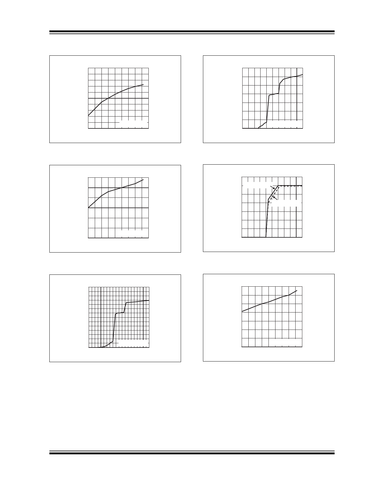
FIGURE 2-7:
Ground Pin Current.
FIGURE 2-8:
Ground Pin Current.
FIGURE 2-9:
Ground Pin Current.
FIGURE 2-10:
Ground Pin Current.
FIGURE 2-11:
Dropout Characteristics.
FIGURE 2-12:
Dropout Voltage.
95
97
99
101
103
105
107
109
111
113
115
-40 -20 0 20 40 60 80 100120140
(
T
N
E
R
R
U
C
D
N
U
O
R
Gμ
)
A
TEMPERATURE (°C)
I
LOAD
= 100μA
95
100
105
110
115
120
125
-40 -20 0 20 40 60 80 100120140
(
T
N
E
R
R
U
C
D
N
U
O
R
Gμ
)
A
TEMPERATURE (°C)
I
LOAD
= 150mA
0
20
40
60
80
100
120
140
0 0.5 1 1.5 2 2.5 3 3.5 4 4.5 5
(
T
N
E
R
R
U
C
D
N
U
O
R
Gμ
)
A
INPUT VOLTAGE (V)
I
LOAD
= 100μA
0
20
40
60
80
100
120
140
0 0.5 1 1.5 2 2.5 3 3.5 4 4.5 5
(
T
N
E
R
R
U
C
D
N
U
O
R
Gμ
)
A
INPUT VOLTAGE (V)
I
LOAD
= 150mA
0
0.5
1.0
1.5
2.0
2.5
3.0
3.5
0 0.5 1 1.5 2 2.5 3 3.5 4 4.5 5
)
V(
E
G
A
T
L
O
V
T
U
P
T
U
O
INPUT VOLTAGE (V)
I
LOAD
= 150mA
I
LOAD
= 100μA
0
0.02
0.04
0.06
0.08
0.10
0.12
0.14
-40 -20 0 20 40 60 80 100120140
)
V
m(
E
G
A
T
L
O
V
T
U
O
P
O
R
D
TEMPERATURE (°C)
I
LOAD
= 100μA
MIC5255
DS20005661A-page 8
2016 Microchip Technology Inc.
FIGURE 2-13:
Short Circuit Current
.
FIGURE 2-14:
Output Voltage vs.
Temperature
.
FIGURE 2-15:
Enable Threshold vs.
Temperature.
FIGURE 2-16:
Turn-On Time vs. Bypass
Capacitance
.
FIGURE 2-17:
Line Transient Response
.
FIGURE 2-18:
Load Transient Response
.
400
410
420
430
440
450
460
470
480
490
500
-40 -20 0 20 40 60 80 100120140
)
A
m(
T
N
E
R
R
U
C
TI
U
C
RI
C
T
R
O
H
S
TEMPERATURE (°C)
V
IN
= V
OUT
+ 1V
2.95
2.96
2.97
2.98
2.99
3.00
3.01
3.02
3.03
3.04
3.05
-40 -20 0 20 40 60 80 100120140
)
V(
E
G
A
T
L
O
V
T
U
P
T
U
O
TEMPERATURE (°C)
I
LOAD
= 100μA
0.8
0.85
0.9
0.95
1
1.05
1.1
1.15
1.2
1.25
1.3
-40 -20 0 20 40 60 80 100120140
)
V(
E
G
A
T
L
O
V
D
L
O
H
S
E
R
H
T
E
L
B
A
N
E
TEMPERATURE (°C)
I
LOAD
= 100μA
0
50
100
150
200
250
300
350
400
450
500
100
1000
10000 100000 1000000
(
E
MI
Tμ
)
s
BYPASS CAPACITANCE (pF)
Prop Delay
Rise Time
C
IN
= 1μF Ceramic
C
OUT
= 1μF Ceramic
I
LOAD
= 100μA
C
IN
= 1μF Ceramic
C
OUT
= 1μF Ceramic
C
BYP
= 0.01μF
I
OUT
= 100μA
TIME (400μs/div)
e
g
atl
o
V t
u
pt
u
O
)
vi
d/
V
m
0
5(
e
g
atl
o
V t
u
p
nI
)
vi
d/
V
1(
4V
5V
C
IN
= 1μF Ceramic
C
OUT
= 1μF Ceramic
C
BYP
= 0.01μF
V
IN
= 4V
100μA
150mA
TIME (4μs/div)
t
n
er
r
u
C t
u
pt
u
O
)
vi
d/
A
m
0
0
1(
e
g
atl
o
V t
u
pt
u
O
)
vi
d/
V
m
0
5(
2016 Microchip Technology Inc.
DS20005661A-page 9
MIC5255
FIGURE 2-19:
Enable Pin Delay.
FIGURE 2-20:
Shutdown Delay.
C
IN
= 1μF Ceramic
C
OUT
= 1μF Ceramic
C
BYP
= 0.01μF
I
OUT
= 100μA
TIME (10μs/div)
e
g
atl
o
V t
u
pt
u
O
)
vi
d/
V
1(
e
g
atl
o
V
el
b
a
n
E
)
vi
d/
V
1(
C
IN
= 1μF Ceramic
C
OUT
= 1μF Ceramic
C
BYP
= 0.01μF
V
IN
= 4V
TIME (400μs/div)
e
g
atl
o
V t
u
pt
u
O
)
vi
d/
V
1(
e
g
atl
o
V
el
b
a
n
E
)
vi
d/
V
1(
MIC5255
DS20005661A-page 10
2016 Microchip Technology Inc.
3.0
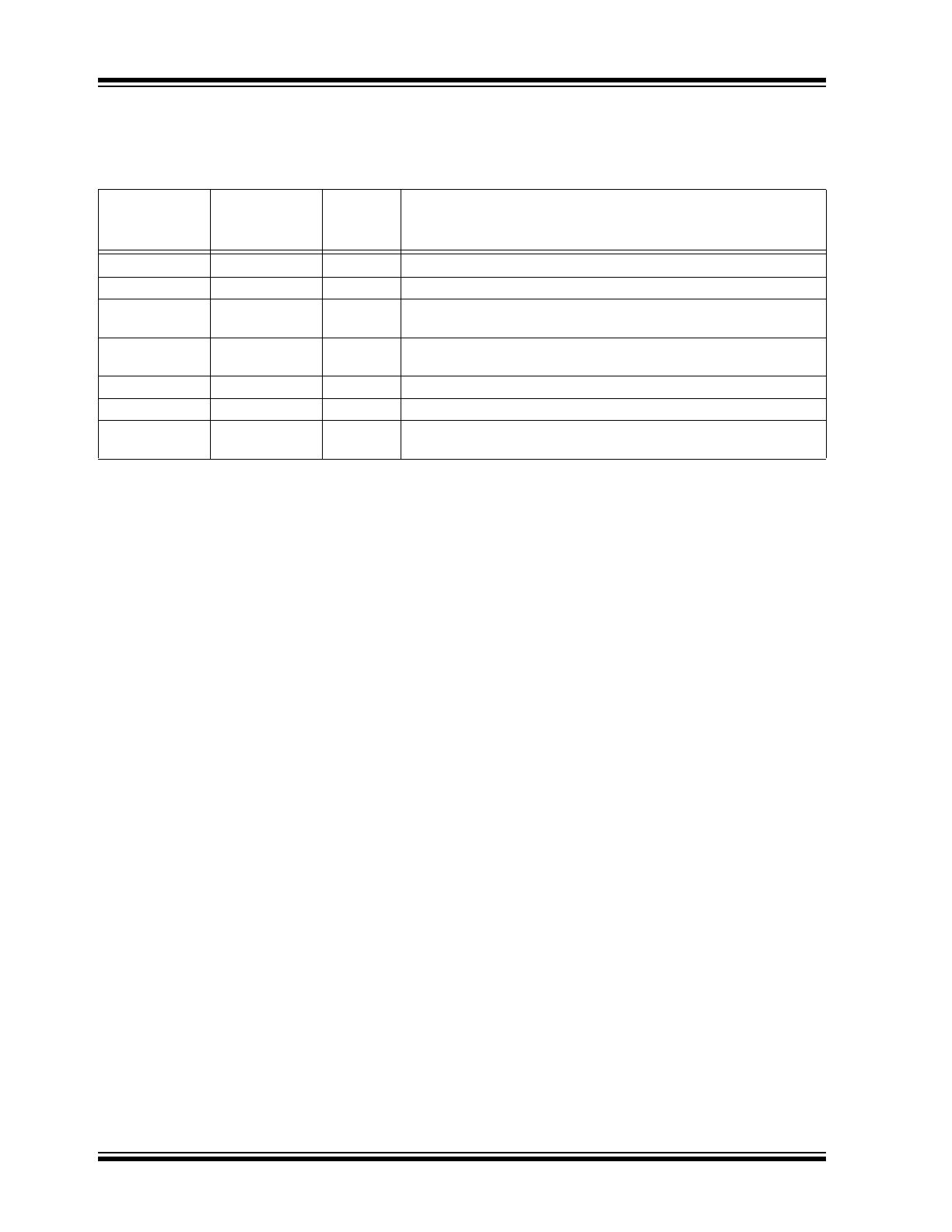
PIN DESCRIPTIONS
The descriptions of the pins are listed in
Table 3-1
.
TABLE 3-1:
PIN FUNCTION TABLE
Pin Number
SOT23-5
TSOT23-5
Pin Number
VDFN-6
Pin Name
Description
1
3
IN
Supply Input.
2
2
GND
Ground.
3
1
EN
Enable/Shutdown (Input): CMOS-compatible input. Logic-high =
enable; logic-low = shutdown. Do not leave open.
4
6
BYP
Reference Bypass: Connect external 0.01 µF ≤ C
BYP
≤ 1.0 µF
capacitor to GND to reduce output noise. May be left open.
5
4
OUT
Regulator Output.
—
5
NC
No internal connection.
—
EP
GND
Ground: Internally connected to the exposed pad. Connect
externally to GND pin.