
2017 Microchip Technology Inc.
DS20005919A-page 1
MIC23156
Features
• Input Voltage: 2.7V to 5.5V
• Up to 1.5A Output Current
• 1 MHz I
2
C Controlled Adjustable Output:
- V
OUT
= 0.7 to 2.4V in 10 mV Steps
• High Output Voltage Accuracy
(±1.5% over Temperature)
• Fast Pin-Selectable Output Voltage
• Programmable Soft-Start Using External Capaci-
tor
• Ultra-Low Quiescent Current of 30 µA when
Not Switching
• Thermal Shutdown and Current-Limit Protection
• Safe Start-Up into Pre-Biased Output
• Stable with 1 µH Output Inductor and
2.2 µF Ceramic Capacitor
• Up to 93% Peak Efficiency
• –40°C to +125°C Junction Temperature Range
• Available in 16-ball, 0.4 mm pitch, 1.81 mm x
1.71 mm Wafer Level Chip-Scale (WLCSP) and
17-pin, 2.8 mm x 2.5 mm QFN Packages
Applications
• Mobile Handsets
• Solid-State Drives (SSD)
• WiFi/WiMx/WiBro Modules
• Portable Applications
General Description
The MIC23156 is a high-efficiency, 1.5A synchronous
buck regulator with HyperLight Load
®
mode and
dynamic voltage scaling control through I
2
C. HyperLight
Load provides very high efficiency at light loads and
ultra-fast transient response. The ability to dynamically
change the output voltage and maintain high output volt-
age accuracy make the MIC23156 perfectly suited for
supplying processor core voltages. An additional benefit
of this proprietary architecture is very low output ripple
voltage, throughout the entire load range, with the use of
small output capacitors. Fast mode plus I
2
C provides
output voltage and chip enable/disable control from a
standard I
2
C bus with I
2
C clock rates of 100 kHz,
400 kHz, and 1 MHz.
The MIC23156 is designed for use with 1 µH, and an
output capacitor as small as 2.2 µF, that enables a total
solution size less than 1 mm in height.
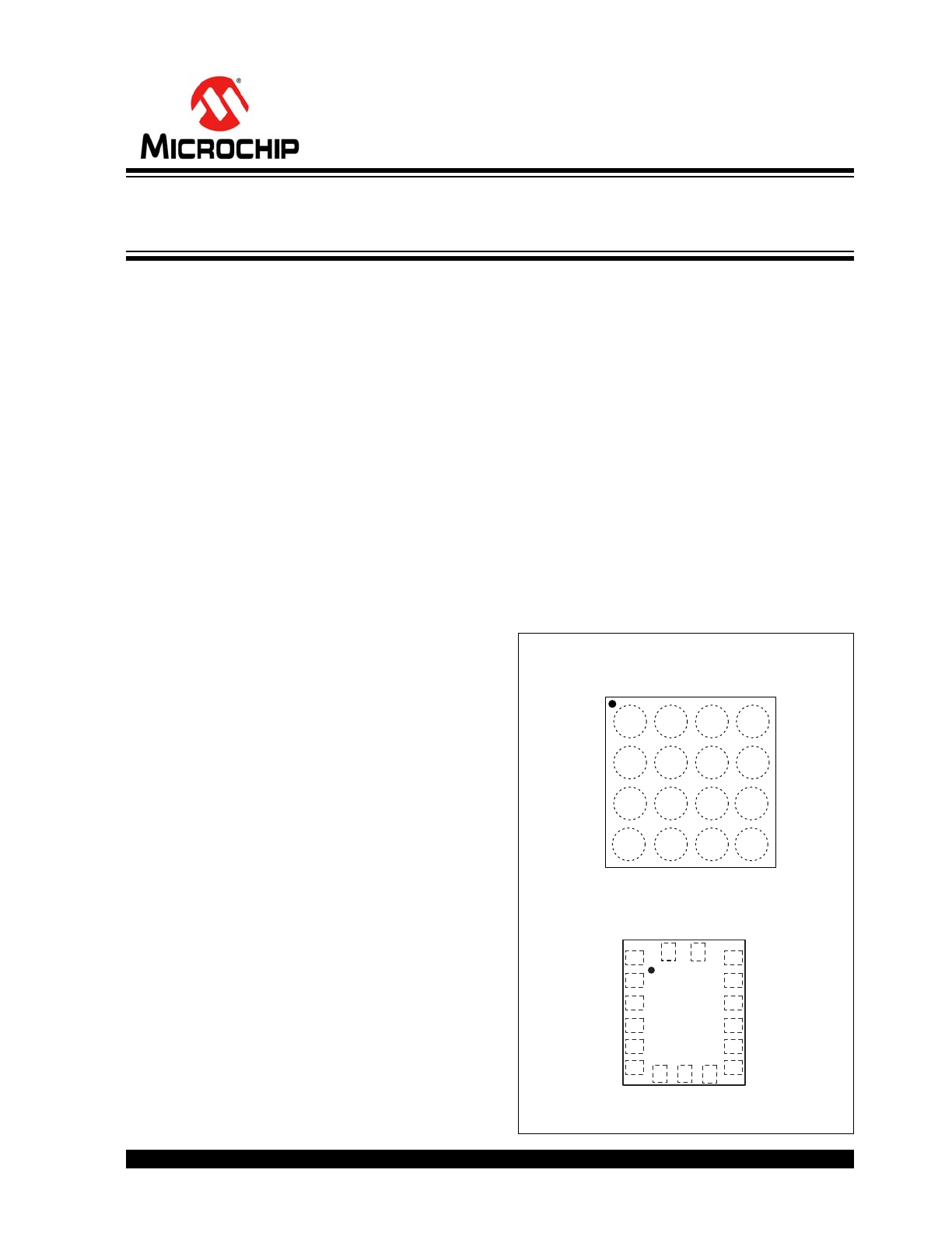
Package Types
A
D
C
B
1
2
SS
4
3
SNS
SDA
SCL
VI2C
VSEL
AGND
AVIN
PGOOD
PVIN
SW
SW
PGND
PGND
PVIN
EN
16-Ball 1.81 mm x 1.71 mm WLCSP (CS)
(Top View)
SS
V
SEL
8
V
I2C
SCL
SDA
SNS
1
PGND
PGND
PV
IN
PV
IN
2
3
4
9
5
NC
EN
7
6
SW
SW
PGOOD
AV
IN
AGND
10
12
11
13
14
15
16
17
17-Pin 2.5 mm x 2.8 mm QFN (ML)
(Top View)
1.5A, 3 MHz Synchronous Buck Regulator with HyperLight Load
®
and I
2
C Control for Dynamic Voltage Scaling
MIC23156
DS20005919A-page 2
2017 Microchip Technology Inc.
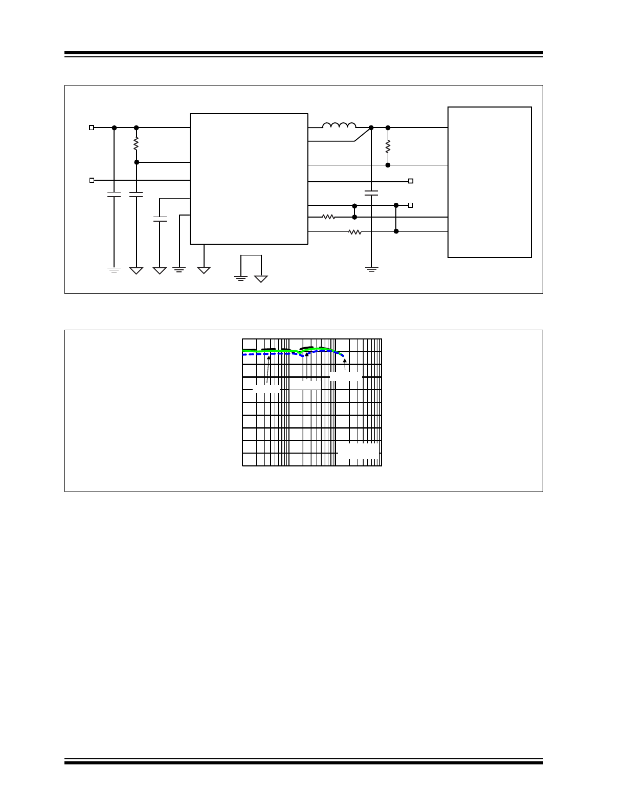
Typical Application Schematic
Efficiency (V
OUT
= 2.4V) vs. Output Current
V
IN
EN
PV
IN
AV
IN
EN
SS
PGND
AGND
SW
SNS
PGOOD
V
SEL
V
I2C
SCL
SDA
APPLICATIONS
V
SEL
V
I2C
U1
MIC23156
PROCESSOR
CORE
SUPPLY
POR
I
2
C HIGH-SPEED
MODE BUS
0
10
20
30
40
50
60
70
80
90
100
10
100
1000
10000
OUTPUT CURRENT (mA)
V
IN
= 3.6V
V
IN
= 5V
V
IN
= 4.2V
C
OUT
= 2.2 µF
L = 1 µH
EFFICIENCY
(%)
2017 Microchip Technology Inc.
DS20005919A-page 3
MIC23156
1.0
ELECTRICAL CHARACTERISTICS
Absolute Maximum Ratings
†
Input Supply Voltage (AV
IN
, PV
IN
, V
I2C
)....................................................................................................... –0.3V to +6V
Switch Voltage (SW) ....................................................................................................................................–0.3V to AV
IN
Logic Voltage (EN, PGOOD)........................................................................................................................–0.3V to AV
IN
Logic Voltage (V
SEL
, SCL, SDA).................................................................................................................. –0.3V to V
I2C
Analog Input Voltage (SNS, SS) ..................................................................................................................–0.3V to AV
IN
Power Dissipation (T
A
= +70°C)............................................................................................................. Internally Limited
ESD Rating
(
1
)
............................................................................................................................................................. 2 kV
Note 1:
Devices are ESD-sensitive. Handling precautions are recommended. Human body model, 1.5 k
in series
with 100 pF.
Operating Ratings
(
1
)
Input Supply Voltage (AV
IN
, PV
IN
, V
I2C
).................................................................................................... +2.7V to +5.5V
Switch Voltage (SW) .........................................................................................................................................0V to AV
IN
Logic Voltage (EN, PGOOD).............................................................................................................................0V to AV
IN
Logic Voltage (V
SEL
, SCL, SDA)....................................................................................................................... 0V to V
I2C
Analog Input Voltage (SNS, SS) .......................................................................................................................0V to AV
IN
Note 1:
The device is not ensured to function outside the operating range.
†
Notice:
Stresses above those listed under “Maximum Ratings” may cause permanent damage to the device. This
is a stress rating only and functional operation of the device at those or any other conditions above those indi-
cated in the operational sections of this specification is not intended. Exposure to maximum rating conditions for
extended periods may affect device reliability.
MIC23156
DS20005919A-page 4
2017 Microchip Technology Inc.
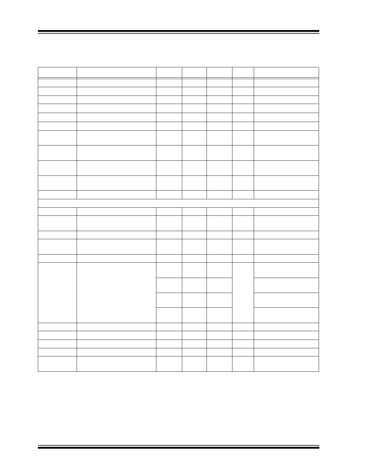
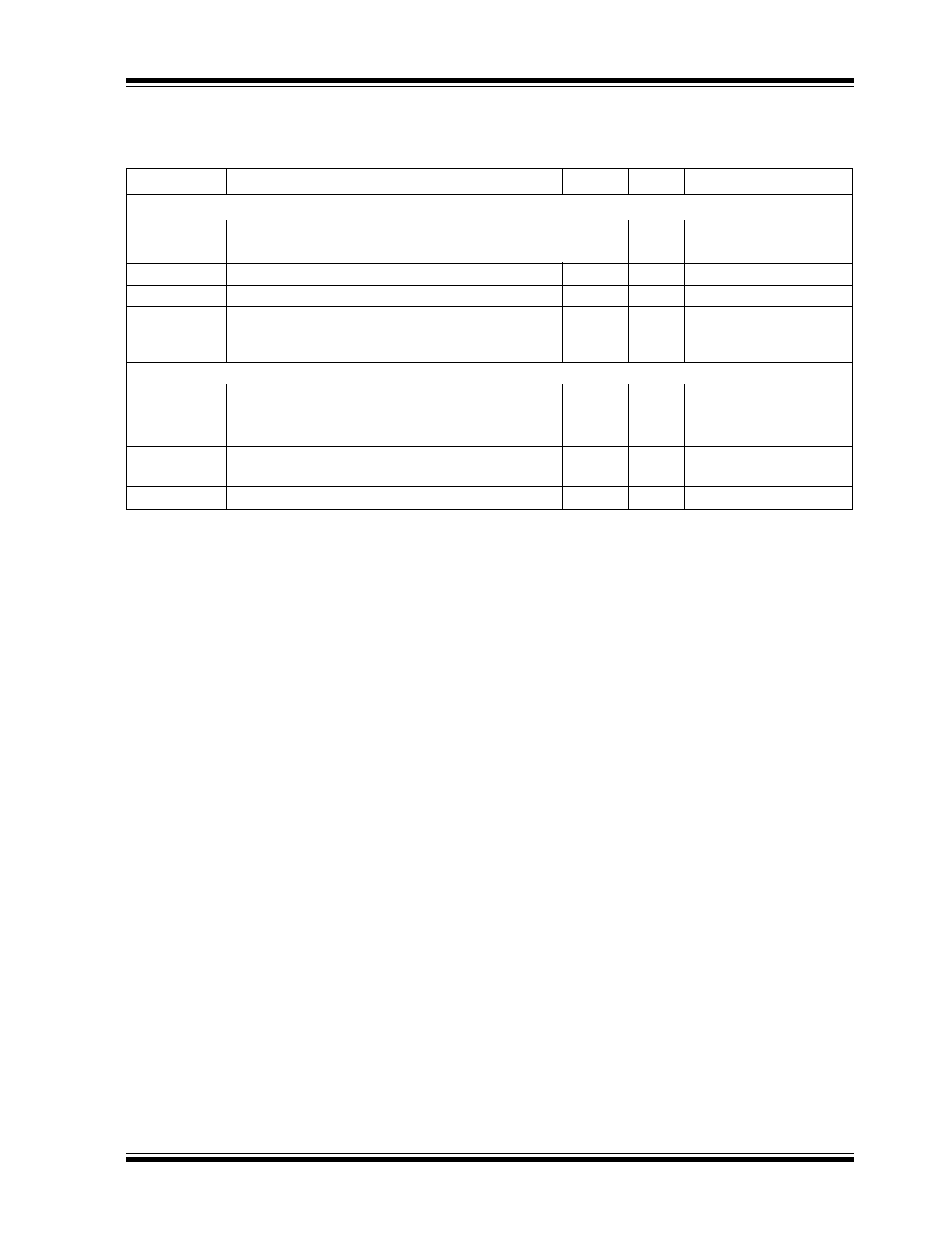
TABLE 1-1:
ELECTRICAL CHARACTERISTICS
(
1
)
Electrical Specifications:
unless otherwise specified, T
A
= +25°C; AV
IN
= PV
IN
= V
EN
= V
VI2C
= 3.6V; L = 1.0 µH; C
OUT
= 2.2
µF. Boldface values indicate –40°C
T
J
+125°C.
Symbol
Parameter
Min.
Typ.
Max.
Units
Test Conditions
V
IN
Supply Input Voltage Range
2.7
—
5.5
V
—
EN
LOW
Enable Logic Pin Low Threshold
—
—
0.5
V
Logic low
EN
HIGH
Enable Logic Pin High Threshold
1.2
—
—
V
Logic high
I
VSEL_LO
V
SEL
Logic Pin Low Threshold
—
—
0.3 x V
I2C
V
Logic low
I
VSEL_HI
V
SEL
Logic Pin High Threshold
0.7 x V
I2C
—
—
V
Logic high
I
EN
Logic Pin Input Current
—
0.1
2
µA
Pins: EN and V
SEL
UVLO
Undervoltage Lockout
Threshold
2.45
2.55
2.65
V
Rising
UVLO_HYS
Undervoltage Lockout
Hysteresis
—
75
—
mV
Falling
T
SHD
Shutdown Temperature
(Threshold)
—
160
—
°C
—
T
SHD_HYST
Shutdown Temperature
Hysteresis
—
20
—
°C
—
I
SHDN
Shutdown Supply Current
—
0.1
5
µA
V
EN
= 0V
DC-to-DC Converter
V
OUT
Output Voltage Accuracy
–1.5
—
+1.5
%
V
OUT
= 1V, I
OUT
= 10 mA
I
Q
Quiescent Supply Current
—
30
50
µA
I
OUT
= 0 mA,
V
FB
> 1.2 * V
OUT
V
OUT
Output Voltage Range
0.7
—
2.4
V
V
OUT
/V
OUT
Output Voltage Line Regulation
—
0.02
—
%/V
3.0V < V
AVIN
< 4.5V,
I
LOAD
= 10 mA
V
OUT
/V
OUT
Output Voltage Load Regulation
—
0.04
—
%
20 mA < I
OUT
< 1A
R
SWON
Switch-On Resistance
—
0.17
—
Ω
I
SW
= +100 mA, high-side
switch PMOS (QFN)
—
0.15
—
I
SW
= +100 mA, high-side
switch PMOS (WLCSP)
—
0.15
—
I
SW
= –100 mA, low-side
switch NMOS (QFN)
—
0.13
—
I
SW
= –100 mA, low-side
switch NMOS (WLCSP)
I
LIM
Current Limit (DC Value)
1.7
2.9
5.1
A
V
OUT
= 1V
f
SW
Oscillator Switching Frequency
—
3
—
MHz
—
D
MAX
Maximum Duty Cycle
80
—
—
%
Frequency = 3 MHz
—
DVS Step-Size
—
19
—
mV
—
t
SS
Soft Start Time
—
250
—
µs
V
OUT
= 90%,
C
SS
= 120 pF
Note 1:
Specifications are for packaged product only.
2017 Microchip Technology Inc.
DS20005919A-page 5
MIC23156
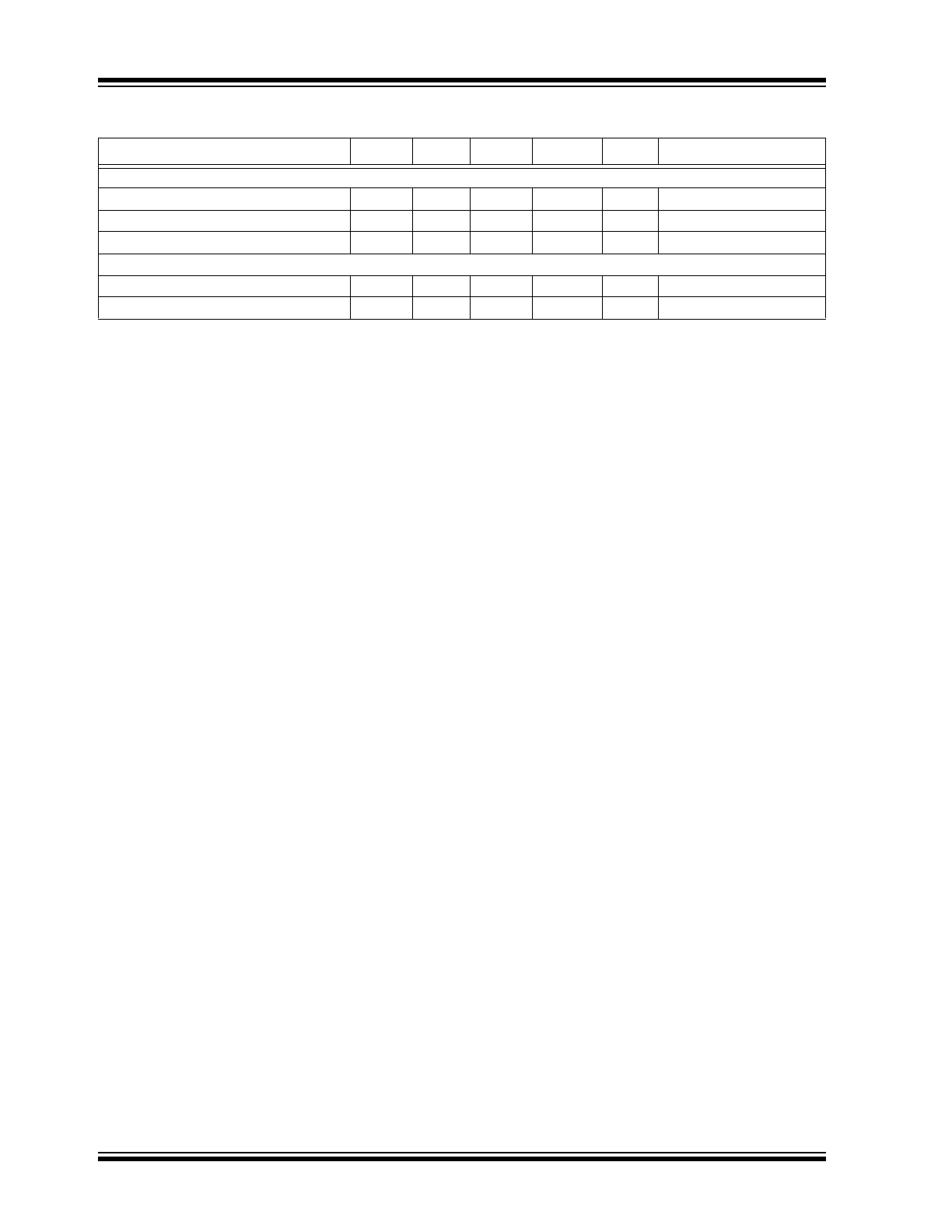
I
2
C Interface (Assuming 550 pF Total Bus Capacitance
I
2
C Address
10110111
, 0xB7
—
Read (Binary, Hex)
10110110
, 0xB6
Write (Binary, Hex)
V
IL
Low-Level Input Voltage
—
—
0.3 x V
I2C
V
SCL, SDA
V
IH
High-Level Input Voltage
0.7 x V
I2C
—
—
V
SCL, SDA
R
SDA_PD
SDA Pull-Down Resistance
—
20
—
W
Open-drain pull-down on
SDA during read back,
I
SDA
= 500 µA
Power Good (PG)
V
PG_LOW
PGOOD Output Low
—
100
—
mV
V
OUT
< 80% V
NOM
,
I
PGOOD
= -500 µA
I
PG_LEAK
PGOOD Output Leakage
—
—
5
µA
V
OUT
= V
NOM
V
PG_TH
PGOOD Threshold
(% of V
OUT
< V
NOM
)
86
—
96
%
V
OUT
ramping up
V
PG_HYS
PGOOD Hysteresis
—
5
—
%
—
TABLE 1-1:
ELECTRICAL CHARACTERISTICS
(
1
)
(CONTINUED)
Electrical Specifications:
unless otherwise specified, T
A
= +25°C; AV
IN
= PV
IN
= V
EN
= V
VI2C
= 3.6V; L = 1.0 µH; C
OUT
= 2.2
µF. Boldface values indicate –40°C
T
J
+125°C.
Symbol
Parameter
Min.
Typ.
Max.
Units
Test Conditions
Note 1:
Specifications are for packaged product only.
MIC23156
DS20005919A-page 6
2017 Microchip Technology Inc.
TEMPERATURE SPECIFICATIONS (
Note 1
)
Parameters
Symbol
Min.
Typ.
Max.
Units
Conditions
Temperature Ranges
Storage Temperature
T
S
–65
—
+150
°C
—
Lead Temperature
—
—
—
+260
°C
Soldering, 10 sec.
Junction Temperature Range
T
J
–40
—
+125
°C
—
Package Thermal Resistances
Thermal Resistance WLCSP 16-Ball
JA
—
150
—
°C/W
—
Thermal Resistance QFN-17
JA
—
89
—
°C/W
—
Note 1:
The maximum allowable power dissipation is a function of ambient temperature, the maximum allowable
junction temperature and the thermal resistance from junction to air (i.e., T
A
, T
J
,
JA
). Exceeding the max-
imum allowable power dissipation will cause the device operating junction temperature to exceed the max-
imum +125°C rating. Sustained junction temperatures above +125°C can impact the device reliability.
2017 Microchip Technology Inc.
DS20005919A-page 7
MIC23156
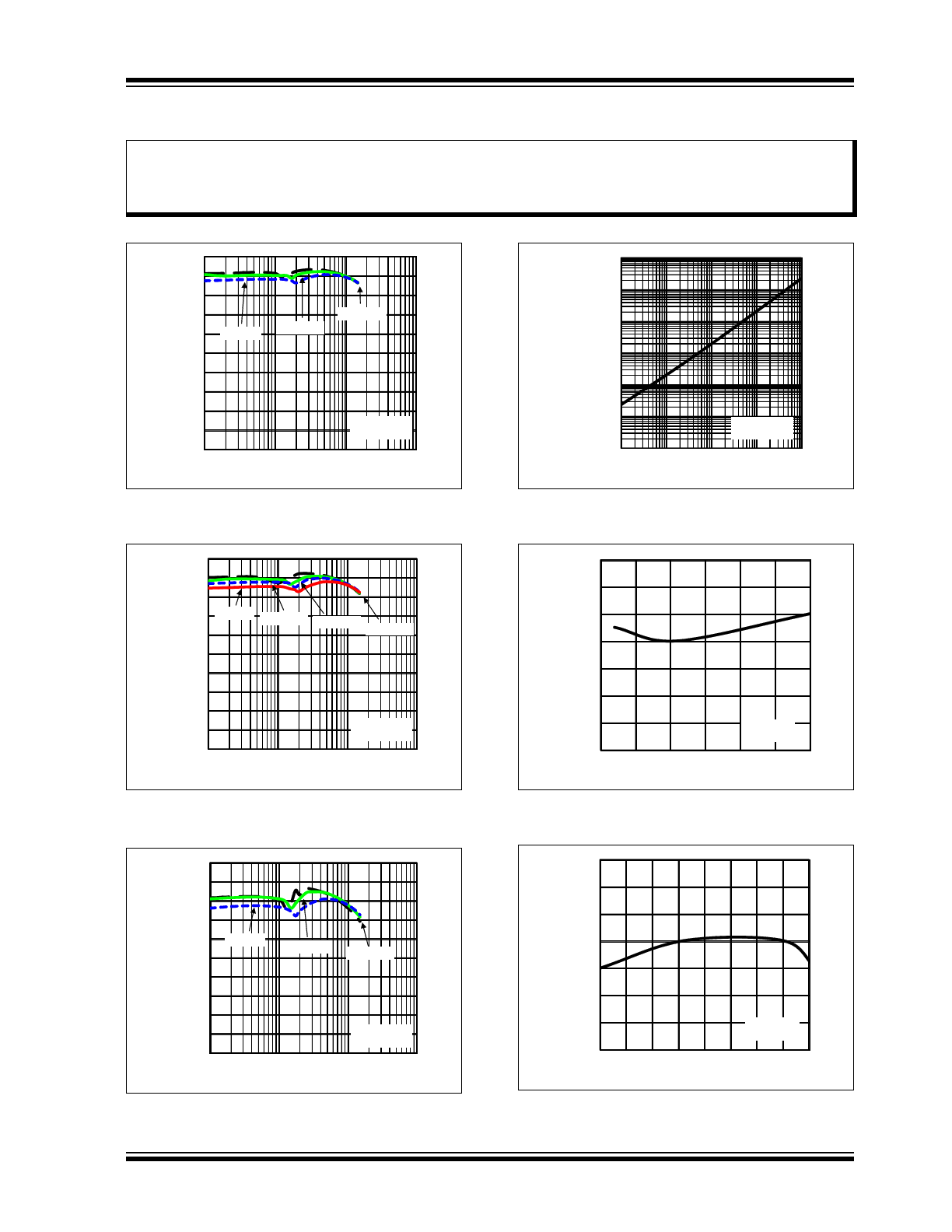
2.0
TYPICAL PERFORMANCE CURVES
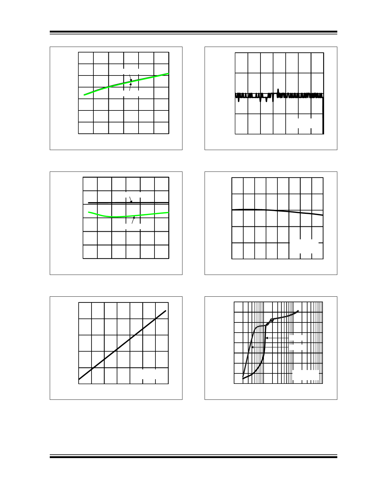
FIGURE 2-1:
Efficiency (V
OUT
= 2.4V) vs.
Output Current.
FIGURE 2-2:
Efficiency (V
OUT
= 1.8V) vs.
Output Current.
FIGURE 2-3:
Efficiency (V
OUT
= 1.0V) vs.
Output Current.
FIGURE 2-4:
V
OUT
Rise Time vs. C
SS
.
FIGURE 2-5:
Current Limit vs. Input
Voltage.
FIGURE 2-6:
Current Limit vs.
Temperature.
Note:
The graphs and tables provided following this note are a statistical summary based on a limited number of
samples and are provided for informational purposes only. The performance characteristics listed herein
are not tested or guaranteed. In some graphs or tables, the data presented may be outside the specified
operating range (e.g., outside specified power supply range) and therefore outside the warranted range.
0
10
20
30
40
50
60
70
80
90
100
10
100
1000
10000
OUTPUT CURRENT (mA)
V
IN
= 3.6V
V
IN
= 5V
V
IN
= 4.2V
C
OUT
= 2.2 µF
L = 1 µH
EF
FICI
EN
CY
(
%
)
0
10
20
30
40
50
60
70
80
90
100
10
100
1000
10000
OUTPUT CURRENT (mA)
V
IN
= 3.6V
V
IN
= 5V
V
IN
= 2.7V
V
IN
= 4.2V
C
OUT
= 2.2 µF
L = 1 µH
EFF
ICIENCY
(%
)
0
10
20
30
40
50
60
70
80
90
100
10
100
1000
10000
OUTPUT CURRENT (mA)
V
IN
= 3.6V
V
IN
= 5V
V
IN
= 2.7V
C
OUT
= 2.2 µF
L = 1 µH
EFF
ICIENCY
(%
)
10
100
1000
10000
100000
1000000
10000000
100
1000
10000
100000
1000000
C
SS
(pF)
V
OUT
= 1.0V
C
OUT
= 2.2 µF
RISE TIME (µs)
2.5
2.6
2.7
2.8
2.9
3.0
3.1
3.2
2.5
3
3.5
4
4.5
5
5.5
INPUT VOLTAGE (V)
T
A
= 25\ C
V
OUT
= 1.0V
CURR
EN
T L
IMIT (
A
)
2.5
2.6
2.7
2.8
2.9
3.0
3.1
3.2
-40
-20
0
20
40
60
80
100
120
TEMPERATURE (
°C)
V
IN
= 3.6V
V
OUT
= 1.0V
CUR
RENT L
IMIT (
A
)
MIC23156
DS20005919A-page 8
2017 Microchip Technology Inc.
FIGURE 2-7:
Quiescent Current vs. Input
Voltage.
FIGURE 2-8:
Shutdown Current vs. Input
Voltage.
FIGURE 2-9:
Line Regulation (CCM).
FIGURE 2-10:
Line Regulation (HLL).
FIGURE 2-11:
Load Regulation.
FIGURE 2-12:
Output Voltage vs.
Temperature.
10
15
20
25
30
35
40
45
2.5
3.0
3.5
4.0
4.5
5.0
5.5
INPUT VOLTAGE (V)
NO SWITCHING
V
OUT
> V
OUTNOM
* 1.2
C
OUT
= 2.2 µF
125\ C
-40\ C
25\ C
QUI
E
SC
EN
T CU
RR
EN
T (µA)
-40°C
25°C
125°C
0
5
10
15
20
25
30
2.5
3
3.5
4
4.5
5
5.5
INPUT VOLTAGE (V)
V
OUT
= 0V
C
OUT
= 2.2 µF
SHUT
DOWN C
URRENT
(n
A)
1.7
1.725
1.75
1.775
1.8
1.825
1.85
1.875
1.9
2.5
3
3.5
4
4.5
5
5.5
INPUT VOLTAGE (V)
V
OUTNOM
= 1.8V
C
OUT
= 2.2 µF
I
OUT
= 1A
I
OUT
= 300 mA
I
OUT
= 1.5A
OUT
P
UT VOL
T
AGE (V)
1.7
1.725
1.75
1.775
1.8
1.825
1.85
1.875
1.9
2.5
3
3.5
4
4.5
5
5.5
INPUT VOLTAGE (V)
I
OUT
= 1 mA
V
OUTNOM
= 1.8V
C
OUT
= 2.2 µF
I
OUT
= 20 mA
I
OUT
= 120 mA
OUT
P
UT V
O
L
T
AGE
(V
)
1.7
1.725
1.75
1.775
1.8
1.825
1.85
1.875
1.9
0
250
500
750
1000
1250
1500
OUTPUT CURRENT (mA)
V
IN
= 3.6V
V
OUTNOM
= 1.8V
C
OUT
= 2.2 µF
OU
TPUT
VOL
T
AGE (V)
0.980
0.985
0.990
0.995
1.000
1.005
1.010
1.015
1.020
-40
-20
0
20
40
60
80
100 120
TEMPERATURE (
°C)
V
IN
= 3.6V
V
OUT
= 1.0V
I
OUT
= 10 mA
OUT
P
UT VOL
T
AGE (V)
2017 Microchip Technology Inc.
DS20005919A-page 9
MIC23156
FIGURE 2-13:
Enable Threshold vs. Input
Voltage.
FIGURE 2-14:
PGOOD Threshold vs. Input
Voltage.
FIGURE 2-15:
Output Voltage vs. DAC
Linearity.
FIGURE 2-16:
Output Voltage vs. DAC
DNL.
FIGURE 2-17:
Switching Frequency vs.
Temperature.
FIGURE 2-18:
Switching Frequency vs.
Output Current.
0.5
0.6
0.7
0.8
0.9
1
1.1
1.2
2.5
3
3.5
4
4.5
5
5.5
INPUT VOLTAGE (V)
ENABLE RISING
ENABLE FALLING
EN
AB
LE T
H
R
E
SH
OLD
(V)
70%
75%
80%
85%
90%
95%
100%
2.5
3
3.5
4
4.5
5
5.5
INPUT VOLTAGE (V)
PGOOD RISING
PGOOD FALLING
PGOOD T
HRESHOL
D
(%)
0.6
1
1.4
1.8
2.2
2.6
0
25
50
75
100
125
150
175
DAC VOLTAGE CODE
I
OUT
= 250 mA
C
OUT
= 2.2 µF
OUTPUT VOL
T
A
GE (V)
9
9.5
10
10.5
11
0
25
50
75
100
125
150
175
DAC VOLTAGE CODE
I
OUT
= 250 mA
C
OUT
= 2.2 µF
OUTPUT
VOL
T
A
GE
(mV)
0
1
2
3
4
5
-40
-20
0
20
40
60
80
100
120
TEMPERATURE (
°C)
V
IN
= 3.6V
V
OUTNOM
= 1.0V
C
OUT
= 2.2 µF
S
W
IT
CH
IN
G F
R
EQUE
NC
Y
(
M
H
z
)
0.0
0.5
1.0
1.5
2.0
2.5
3.0
3.5
4.0
10
100
1000
10000
OUTPUT CURRENT (mA)
V
OUT
= 1.8V
C
OUT
= 2.2 µF
2.2 µH
1.0 µH
SWI
T
CH
IN
G F
R
E
Q
UEN
C
Y
(M
Hz)
MIC23156
DS20005919A-page 10
2017 Microchip Technology Inc.
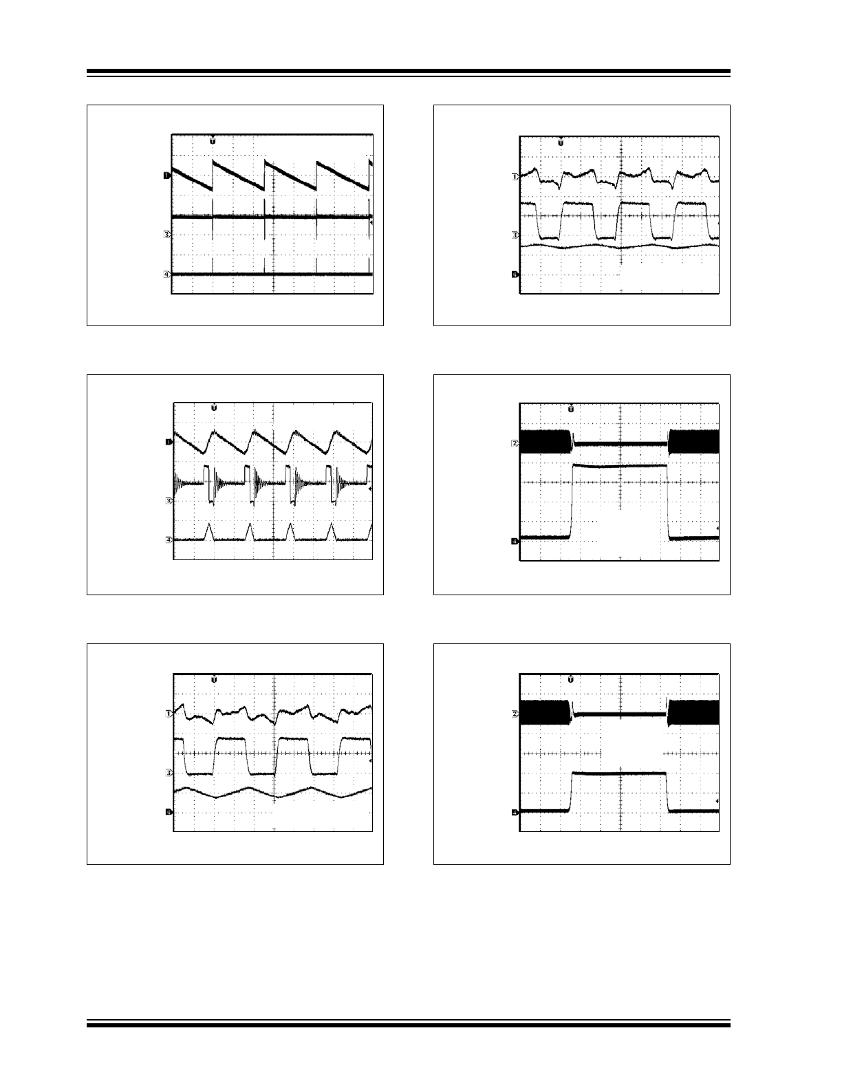
FIGURE 2-19:
Switching Waveform
Discontinuous Mode (1 mA).
FIGURE 2-20:
Switching Waveform
Discontinuous Mode (50 mA).
FIGURE 2-21:
Switching Waveform
Continuous Mode (500 mA).
FIGURE 2-22:
Switching Waveform
Continuous Mode (1.5A).
FIGURE 2-23:
Load Transient (50 mA
to 750 mA).
FIGURE 2-24:
Load Transient (50 mA to 1A).
Time (40 μs/div)
I
L
(500 mA/div)
V
OUT
(AC-COUPLED)
(50 mV/div)
SW
(2V/div)
V
IN
= 3.6V, V
OUT
= 1.8V
C
OUT
= 2.2 μF, L = 1 μH
Time (1 μs/div)
I
L
(500 mA/div)
V
OUT
(AC-COUPLED)
(50 mV/div)
SW
(2V/div)
V
IN
= 3.6V, V
OUT
= 1.8V
C
OUT
= 2.2 μF, L = 1 μH
Time (100 ns/div)
I
L
(500 mA/div)
V
OUT
(AC-COUPLED)
(10 mV/div)
SW
(2V/div)
V
IN
= 3.6V, V
OUT
= 1.8V
C
OUT
= 2.2 μF, L = 1 μH
Time (100 ns/div)
I
L
(1A/div)
V
OUT
(AC-COUPLED)
(10 mV/div)
SW
(2V/div)
V
IN
= 3.6V, V
OUT
= 1.8V
C
OUT
= 2.2 μF, L = 1 μH
Time (40 μs/div)
I
OUT
(200 mA/div)
V
OUT
(AC-COUPLED)
(50 mV/div)
V
IN
= 3.6V
V
OUT
= 1.8V
C
OUT
= 2.2 μF
L = 1 μH
Time (40 μs/div)
I
OUT
(500 mA/div)
V
OUT
(AC-COUPLED)
(50 mV/div)
V
IN
= 3.6V
V
OUT
= 1.8V
C
OUT
= 2.2 μF
L = 1 μH