
IRF5803PbF
V
DSS
R
DS(on)
(max)
I
D
112m
@ V
GS
= -10V
-3.4A
190m
@ V
GS
= -4.5V
-2.7A
- 40V
1
2017-01-27
Absolute Maximum Ratings
Symbol Parameter
Max.
Units
V
DS
Drain-to-Source Voltage
-40
V
I
D
@ T
A
= 25°C
Continuous Drain Current, V
GS
@ -10V
- 3.4
A
I
D
@ T
A
= 70°C
Continuous Drain Current, V
GS
@ -10V
-2.7
I
DM
Pulsed Drain Current -
27
P
D
@T
A
= 25°C
Maximum Power Dissipation 2.0
W
P
D
@T
A
= 70°C
Maximum Power Dissipation 1.3
Linear Derating Factor
16
mW/°C
V
GS
Gate-to-Source Voltage
± 20
T
J
Operating Junction and
°C
T
STG
Storage Temperature Range
-55 to + 150
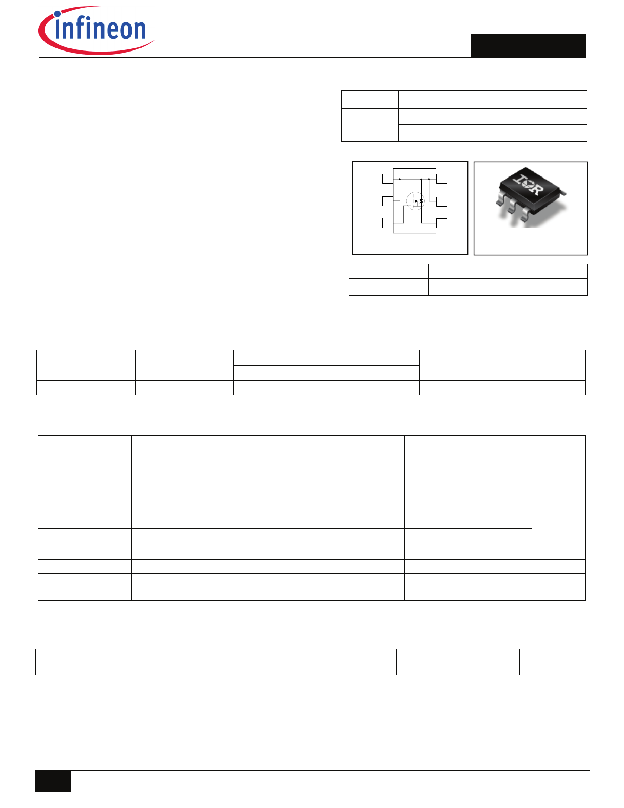
TSOP-6
IRF5803PbF
G D S
Gate Drain Source
Ultra Low On-Resistance
P-Channel
MOSFET
Surface
Mount
Available in Tape & Reel
Low Gate Charge
Lead-Free
Halogen-Free
Base part number
Package Type
Standard Pack
Orderable Part Number
Form
Quantity
IRF5803PbF
TSOP-6
Tape and Reel
3000
IRF5803TRPbF
HEXFET
®
Power MOSFET
Description
These P-channel HEXFET® Power MOSFETs from International
Rectifier utilize advanced processing techniques to achieve the
extremely low on-resistance per silicon area. This benefit
provides the designer with an extremely efficient device for use in
battery and load management applications.
The TSOP-6 package with its customized lead frame produces
a HEXFET® power MOSFET with RDS(on) 60% less than a
similar size SOT-23. This package is ideal for applications where
printed circuit board space is at a premium. It's unique thermal
design and R
DS(on)
reduction enables a current-handling
increase of nearly 300% compared to the SOT-23.
Thermal Resistance
Symbol Parameter
Typ.
Max.
Units
°C/W
R
JA
Junction-to-Ambient –––
62.5
Top View
1
2
D
G
A
D
D
D
S
3
4
5
6
IRF5803PbF
2
2017-01-27
Notes:
Repetitive rating; pulse width limited by max. junction temperature.
Pulse width
400µs; duty cycle 2%.
Surface mounted on 1 in square Cu board
Electrical Characteristics @ T
J
= 25°C (unless otherwise specified)
Parameter Min.
Typ.
Max.
Units
Conditions
V
(BR)DSS
Drain-to-Source Breakdown Voltage
-40
––– –––
V V
GS
= 0V, I
D
= -250µA
V
(BR)DSS
/
T
J
Breakdown Voltage Temp. Coefficient
––– -0.03 ––– V/°C Reference to 25°C, I
D
= -1mA
R
DS(on)
Static Drain-to-Source On-Resistance
––– ––– 112
m
V
GS
= -10V, I
D
= -3.4A
––– ––– 190
V
GS
= -4.5V, I
D
= -2.7A
V
GS(th)
Gate Threshold Voltage
-1.0
––– - 3.0
V V
DS
= V
GS
, I
D
= -250µA
gfs
Forward Trans conductance
4.0
––– –––
S V
DS
= -10V, I
D
= -3.4A
I
DSS
Drain-to-Source Leakage Current
––– ––– -10
µA
V
DS
= -32V, V
GS
= 0V
––– ––– -25
V
DS
= -32V,V
GS
= 0V,T
J
= 150°C
I
GSS
Gate-to-Source Forward Leakage
–––
––– -100
nA
V
GS
= -20V
Gate-to-Source Reverse Leakage
–––
––– 100
V
GS
= 20V
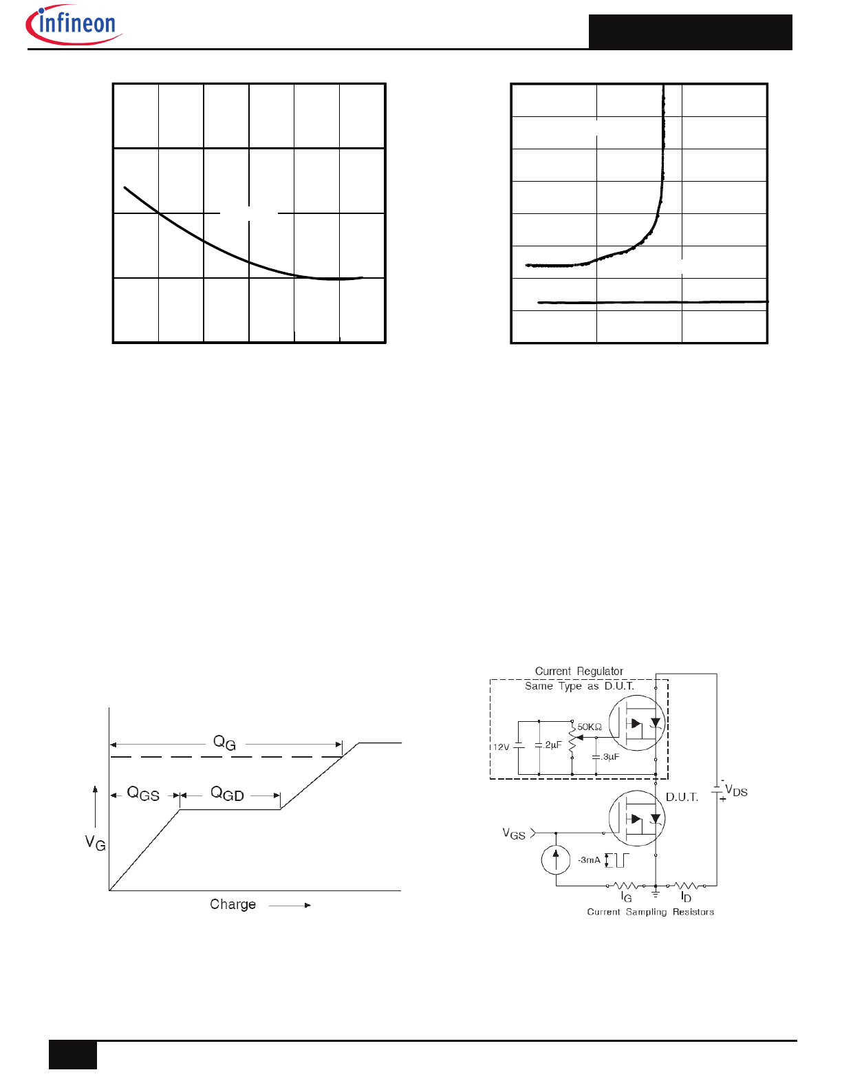
Q
g
Total Gate Charge
–––
25
37
I
D
= -3.4A
Q
gs
Gate-to-Source Charge –––
4.5
6.8
V
DS
= -20V
Q
gd
Gate-to-Drain (‘Miller’) Charge
–––
3.5
5.3
V
GS
= -10V
t
d(on)
Turn-On Delay Time
–––
43
–––
ns
V
DD
= -20V
t
r
Rise Time
–––
550 –––
I
D
= -1.0A
t
d(off)
Turn-Off Delay Time
–––
88
–––
R
G
= 6.0
t
f
Fall Time
–––
50
–––
V
GS
= -10V
C
iss
Input Capacitance
––– 1110 –––
pF
V
GS
= 0V
C
oss
Output Capacitance
–––
93
–––
V
DS
= -25V
C
rss
Reverse Transfer Capacitance
–––
73
–––
ƒ = 100KHz
nC
Source-Drain Ratings and Characteristics
Parameter
Min. Typ. Max. Units
Conditions
I
S
Continuous Source Current
––– ––– -2.0
A
MOSFET symbol
(Body Diode)
showing the
I
SM
Pulsed Source Current
––– ––– -27
integral reverse
(Body Diode)
p-n junction diode.
V
SD
Diode Forward Voltage
–––
––– -1.2
V T
J
= 25°C,I
S
= -2.0A,V
GS
= 0V
t
rr
Reverse Recovery Time
–––
27
40
ns T
J
= 25°C ,I
F
= -2.0A
Q
rr
Reverse Recovery Charge
–––
34
50
nC di/dt = 100A/µs
IRF5803PbF
3
2017-01-27
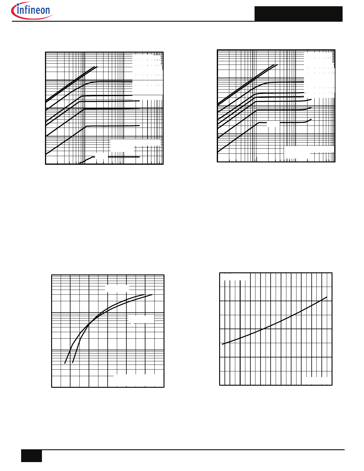
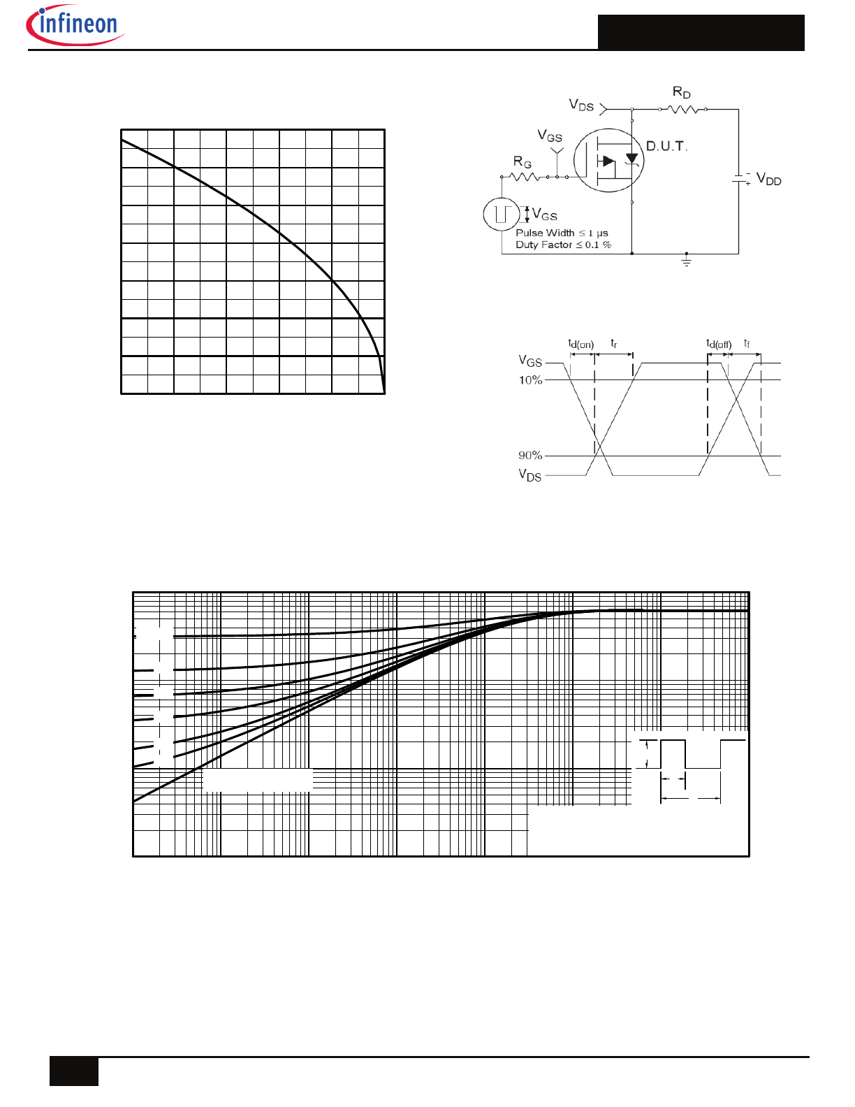
Fig. 2 Typical Output Characteristics
Fig. 3
Typical Transfer Characteristics
Fig. 4 Normalized On-Resistance
vs. Temperature
Fig. 1 Typical Output Characteristics
0.1
1
10
100
-VDS, Drain-to-Source Voltage (V)
0.01
0.1
1
10
100
-I
D
, D
ra
in
-t
o-
S
ou
rc
e
C
ur
re
nt
(
A
)
-2.7V
20µs PULSE WIDTH
Tj = 25°C
VGS
TOP -15V
-10V
-4.5V
-3.7V
-3.5V
-3.3V
-3.0V
BOTTOM - 2.7V
0.1
1
10
100
-VDS, Drain-to-Source Voltage (V)
0.01
0.1
1
10
100
-I
D
, D
ra
in
-t
o-
S
ou
rc
e
C
ur
re
nt
(
A
)
-2.7V
20µs PULSE WIDTH
Tj = 125°C
VGS
TOP -15V
-10V
-4.5V
-3.7V
-3.5V
-3.3V
-3.0V
BOTTOM - 2.7V
0.1
1
10
100
2.0
3.0
4.0
5.0
6.0
7.0
8.0
V = -25V
20µs PULSE WIDTH
DS
-V , Gate-to-Source Voltage (V)
-I
,
D
rai
n-
to
-S
ou
rc
e
Cur
rent
(
A
)
GS
D
T = 25 C
J
°
T = 150 C
J
°
-60 -40 -20 0
20 40 60 80 100 120 140 160
0.0
0.5
1.0
1.5
2.0
T , Junction Temperature ( C)
R
,
D
ra
in
-t
o
-S
o
u
rc
e
O
n
R
e
si
sta
n
ce
(N
o
rm
a
lized)
J
DS(
o
n
)
°
V
=
I =
GS
D
-10V
-3.4A
IRF5803PbF
4
2017-01-27
Fig 5. Typical Capacitance vs.
Drain-to-Source Voltage
Fig 8. Maximum Safe Operating Area
Fig. 7 Typical Source-to-Drain Diode
Forward Voltage
Fig 6. Typical Gate Charge vs.
Gate-to-Source Voltage
1
10
100
VDS, Drain-to-Source Voltage (V)
0
500
1000
1500
2000
C
, C
ap
ac
ita
nc
e(
pF
)
Coss
Crss
Ciss
VGS = 0V, f = 100 KHZ
C iss = Cgs + Cgd , Cds
SHORTED
Crss = Cgd
Coss = Cds + Cgd
0
5
10
15
20
25
30
0
2
4
6
8
10
12
Q , Total Gate Charge (nC)
-V
,
G
at
e
-t
o
-S
o
u
rc
e
V
o
ltage
(V
)
G
GS
I =
D -3.4A
V
=-20V
DS
V
=-32V
DS
0.1
1
10
100
0.4
0.8
1.2
1.6
-V ,Source-to-Drain Voltage (V)
-I
, R
ev
er
se
D
rai
n C
u
rr
en
t (
A
)
SD
SD
V = 0 V
GS
T = 25 C
J
°
T = 150 C
J
°
1
10
100
-VDS , Drain-toSource Voltage (V)
0.1
1
10
100
-I
D
,
D
ra
in
-t
o-
S
ou
rc
e
C
ur
re
nt
(
A
)
TA = 25°C
TJ = 150°C
Single Pulse
1msec
10msec
OPERATION IN THIS AREA
LIMITED BY RDS(on)
100µsec
IRF5803PbF
5
2017-01-27
Fig 11. Maximum Effective Transient Thermal Impedance, Junction-to-Ambient
Fig 9. Maximum Drain Current vs. Case Temperature
Fig 10a. Switching Time Test Circuit
Fig 10b. Switching Time Waveforms
25
50
75
100
125
150
0.0
0.5
1.0
1.5
2.0
2.5
3.0
3.5
T , Case Temperature ( C)
-I
,
D
ra
in C
urr
en
t (A
)
°
C
D
0.1
1
10
100
0.00001
0.0001
0.001
0.01
0.1
1
10
100
Notes:
1. Duty factor D = t / t
2. Peak T = P
x Z
+ T
1
2
J
DM
thJA
A
P
t
t
DM
1
2
t , Rectangular Pulse Duration (sec)
T
herma
l Respo
nse
(Z
)
1
th
JA
0.01
0.02
0.05
0.10
0.20
D = 0.50
SINGLE PULSE
(THERMAL RESPONSE)
IRF5803PbF
6
2017-01-27
Fig 13. Typical On-Resistance Vs.
Drain Current
Fig 14a. Basic Gate Charge Waveform
4.0
8.0
12.0
16.0
-VGS, Gate -to -Source Voltage (V)
0.00
0.05
0.10
0.15
0.20
R
D
S
(o
n)
,
D
ra
in
-t
o
-S
ou
rc
e
O
n
R
es
is
ta
nc
e
(
)
ID = -3.4A
Fig 12. Typical On-Resistance Vs.
Gate Voltage
Fig 14b. Gate Charge Test Circuit
0.0
5.0
10.0
15.0
-ID , Drain Current ( A )
0.00
0.10
0.20
0.30
0.40
R
D
S
(
o
n
) ,
D
ra
in
-t
o-
S
ou
rc
e
O
n
R
es
is
ta
nc
e
(
)
VGS = -4.5V
VGS = -10V
IRF5803PbF
7
2017-01-27
Fig 15. Typical Threshold Voltage Vs.
Junction Temperature
Fig 16. Typical Power Vs. Time
-75
-50
-25
0
25
50
75
100 125 150
TJ , Temperature ( °C )
1.6
2.0
2.4
2.8
-V
G
S
(t
h)
(
V
)
ID = -250µA
0.001
0.010
0.100
1.000
10.000
100.000
Time (sec)
0
5
10
15
20
25
30
P
ow
er
(
W
)
IRF5803PbF
8
2017-01-27
Note: For the most current drawing please refer to Infineon’s web site
www.infineon.com
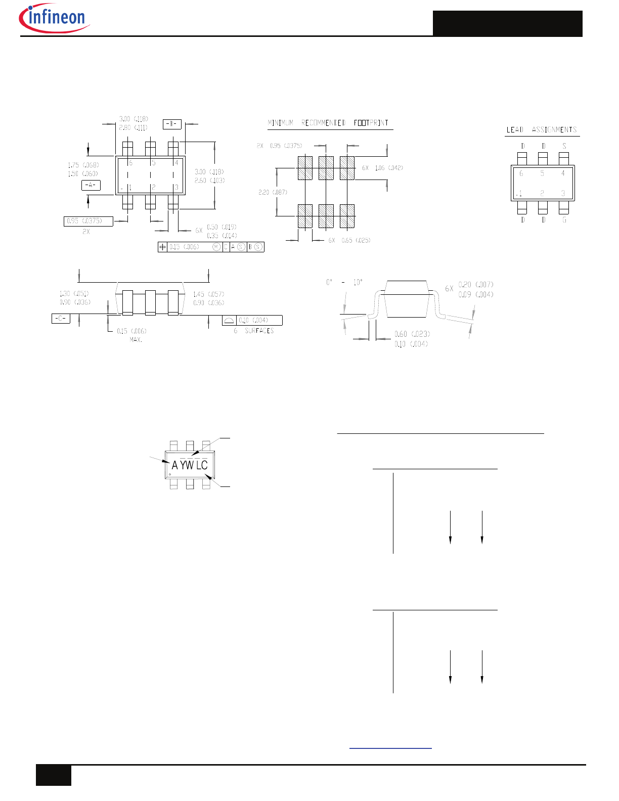
TSOP-6 Part Marking Information
TSOP-6 Package Outline
CODE
TOP
PART NUMBER
W = WEEK
Y = YEAR
LOT
F = IRF5801
(as shown here) indicates Lead-Free.
Note: A line above the work week
A = SI3443DV
B = IRF5800
G = IRF5803
D = IRF5851
E = IRF5852
I = IRF5805
C = IRF5850
N = IRF5802
K = IRF5810
PART NUMBER CODE REFERENCE:
J = IRF5806
H = IRF5804
O = IRLTS6342TRPBF
P = IRFTS8342TRPBF
S = Not applicable
R = IRFTS9342TRPBF
T = IRLTS2242TRPBF
WW = (27-52) IF PRECEDED BY A LETTER
C
H
K
J
E
F
G
D
0
2010
YEAR
B
A
Y
2007
2008
2009
2006
2005
2003
2004
2001
2002
5
7
9
8
6
3
4
1
2
C
29
Z
52
50
51
X
Y
30
D
X
24
W
WORK
WEEK
27
28
B
A
26
25
Z
Y
03
04
01
02
C
D
A
B
DATE CODE MARKING INSTRUCTIONS
WW = (1-26) IF PRECEDED BY LAST DIGIT OF CALENDAR YEAR
YEAR
Y
W
WEEK
WORK
2020
2017
2018
2019
2016
2015
2013
2014
2011
2012
2010
2007
2008
2009
2006
2005
2003
2004
2001
2002
2020
2017
2018
2019
2016
2015
2013
2014
2011
2012
IRF5803PbF
9
2017-01-27
TSOP-6 Tape & Reel Information
Note: For the most current drawing please refer to Infineon’s web site
www.infineon.com
IRF5803PbF
10
2017-01-27
Revision History
Date Comments
01/27/2017
Changed datasheet with Infineon logo-all pages
Updated package outline and part marking on page 8.
Added disclaimer on last page.
Qualification Information
Qualification Level
Consumer
(per JEDEC JESD47F)
†
Moisture Sensitivity Level
TSOP-6
MSL1
(per JEDEC J-STD-020D)
†
RoHS Compliant
Yes
† Applicable version of JEDEC standard at the time of product release.
Trademarks of Infineon Technologies AG
µHVIC™, µIPM™, µPFC™, AU-ConvertIR™, AURIX™, C166™, CanPAK™, CIPOS™, CIPURSE™, CoolDP™, CoolGaN™, COOLiR™, CoolMOS™, CoolSET™,
CoolSiC™, DAVE™, DI-POL™, DirectFET™, DrBlade™, EasyPIM™, EconoBRIDGE™, EconoDUAL™, EconoPACK™, EconoPIM™, EiceDRIVER™, eupec™, FCOS™,
GaNpowIR™, HEXFET™, HITFET™, HybridPACK™, iMOTION™, IRAM™, ISOFACE™, IsoPACK™, LEDrivIR™, LITIX™, MIPAQ™, ModSTACK™, my-d™, NovalithIC™,
OPTIGA™, OptiMOS™, ORIGA™, PowIRaudio™, PowIRStage™, PrimePACK™, PrimeSTACK™, PROFET™, PRO-SIL™, RASIC™, REAL3™, SmartLEWIS™, SOLID
FLASH™, SPOC™, StrongIRFET™, SupIRBuck™, TEMPFET™, TRENCHSTOP™, TriCore™, UHVIC™, XHP™, XMC™
Trademarks updated November 2015
Other Trademarks
All referenced product or service names and trademarks are the property of their respective owners.
Edition 2016-04-19
Published by
Infineon Technologies AG
81726 Munich, Germany
© 2016 Infineon Technologies AG.
All Rights Reserved.
Do you have a question about this
document?
Email:
erratum@infineon.com
Document reference
ifx1
IMPORTANT NOTICE
The information given in this document shall in no
event be regarded as a guarantee of conditions or
characteristics (“Beschaffenheitsgarantie”) .
With respect to any examples, hints or any typical
values stated herein and/or any information
regarding the application of the product, Infineon
Technologies hereby disclaims any and all
warranties and liabilities of any kind, including
without limitation warranties of non-infringement
of intellectual property rights of any third party.
In addition, any information given in this
document is subject to customer’s compliance
with its obligations stated in this document and
any applicable legal requirements, norms and
standards concerning customer’s products and
any use of the product of Infineon Technologies in
customer’s applications.
The data contained in this document is exclusively
intended for technically trained staff. It is the
responsibility of customer’s technical
departments to evaluate the suitability of the
product for the intended application and the
completeness of the product information given in
this document with respect to such application.
For further information on the product, technology,
delivery terms and conditions and prices please
contact your nearest Infineon Technologies office
(
www.infineon.com
).
Please note that this product is not qualified
according to the AEC Q100 or AEC Q101 documents
of the Automotive Electronics Council.
WARNINGS
Due to technical requirements products may
contain dangerous substances. For information on
the types in question please contact your nearest
Infineon Technologies office.
Except as otherwise explicitly approved by Infineon
Technologies in a written document signed by
authorized representatives of Infineon
Technologies, Infineon Technologies’ products
may not be used in any applications where a
failure of the product or any consequences of the
use thereof can reasonably be expected to result in
personal injury.