
2017 Microchip Technology Inc.
DS20005827A-page 1
HV257
Features
• Thirty-two Independent High-voltage Amplifiers
• 300V Operating Voltage
• 295V Output Voltage
• 2.2V/µs Typical Output Slew Rate
• Adjustable Output Current Source Limit
• Adjustable Output Current Sink Limit
• Internal Closed-loop Gain of 72V/V
• 12 MΩ Feedback Impedance
• Layout Ideal for Die Applications
Applications
• Microelectromechanical Systems (MEMS) Driver
• Piezoelectric Transducer Driver
• Optical Crosspoint Switches
(Using MEMS Technology)
General Description
The
HV257 is a 32-channel, high-voltage
sample-and-hold amplifier array integrated circuit. It
operates on a single high-voltage supply, up to 300V,
and two low-voltage supplies, V
DD
and V
NN
.
All 32 sample-and-hold circuits share a common
analog input, V
SIG
. The individual sample-and-hold
circuits are selected by a five-to-32 logic decoder. The
sampled voltage on the holding capacitor is buffered by
a low-voltage amplifier and is magnified by a
high-voltage amplifier with a closed-loop gain of 72V/V.
The internal closed-loop gain is set for an input voltage
range of 0V to 4.096V. The input voltage can be up to
5V, but the output will saturate. The maximum output
voltage swing is 5V below the V
PP
high-voltage supply.
The outputs can drive capacitive loads of up to
3000 pF.
The maximum output source and sink current can be
adjusted by using two external resistors. An external
R
SOURCE
resistor controls the maximum sourcing
current, and an external R
SINK
resistor controls the
maximum sinking current. The current limit is
approximately 12.5V divided by the external resistor
value. The setting is common for all 32 outputs. A
low-voltage silicon junction diode is made available to
help monitor the die temperature.
Package Type
100-lead MQFP
(Top view)
1
100
See
Table 3-1
for pin information.
32-Channel High-Voltage Sample-and-Hold Amplifier Array
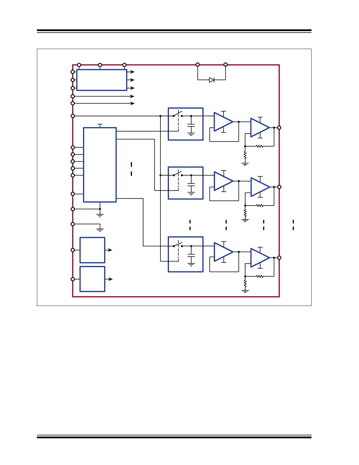
R
HV
OUT
0
AV
NN
AV
DD
S/H-0
5 to 32
Decoder
VSIG
A
0
A
1
A
2
A
3
EN
A
4
R
S/H-1
HV
OUT
1
R
S/H-31
HV
OUT
31
V
PP
AV
DD
AV
NN
AV
NN
C
H
-
+
-
+
Q
0
Q
1
Q
31
HV
OUT
Current
Sink
Limiting
To all HV
OUT
amplifiers
RSOURCE
RSINK
DVDD
AVNN
DGND
AGND
VPP
AVDD
To internal VPP bus
To internal analog VDD bus
To internal analog VNN bus
To internal digital VDD bus
To internal digital VNN bus
DV
DD
DVNN
AV
DD
AV
NN
C
H
C
H
BYP-VPP BYP-AVDD BYP-AVNN Anode Cathode
Bias Circuit
-
+
-
+
-
+
-
+
HV
OUT
Current
Source
Limiting
To all HV
OUT
amplifiers
71R
V
PP
AV
NN
71R
V
PP
AV
NN
71R
HV257
DS20005827A-page 2
2017 Microchip Technology Inc.
Functional Block Diagram
2017 Microchip Technology Inc.
DS20005827A-page 3
HV257
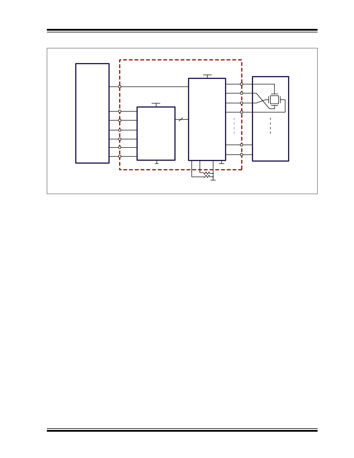
Typical Application Circuit
VSIG
A0
EN
A3
A2
A4
HV
OUT
0
HV257
High Voltage
Power Supply
Low Voltage
Power Supply
32
DGND
AGND
HV
OUT
1
MEMS
Array
y
y
x
x
HV
OUT
2
HV
OUT
3
HV
OUT
30
HV
OUT
31
A1
VNN
Low Voltage
Channel
Select
Sample
and Hold
High
Voltage
OpAmp
Array
RSOURCE
RSINK
Micro
Processor
DAC
HV257
DS20005827A-page 4
2017 Microchip Technology Inc.
1.0
ELECTRICAL CHARACTERISTICS
Absolute Maximum Ratings†
High-voltage Supply, V
PP
....................................................................................................................................... 310V
Analog Low-voltage Positive Supply, AV
DD
................................................................................................................ 8V
Digital Low-voltage Positive Supply, DV
DD
................................................................................................................. 8V
Analog Low-voltage Negative Supply, AV
NN
............................................................................................................ –7V
Digital Low-voltage Negative Supply, DV
NN
............................................................................................................ –7V
Logic Input Voltage.................................................................................................................................. –0.5V to DV
DD
Analog Input Signal, V
SIG
................................................................................................................................. 0V to 6V
Maximum Junction Temperature, T
J
..................................................................................................................... 150°C
Storage Temperature, T
S
.................................................................................................................... –65°C to +150°C
† Notice: Stresses above those listed under “Absolute Maximum Ratings” may cause permanent damage to the
device. This is a stress rating only, and functional operation of the device at those or any other conditions above those
indicated in the operational sections of this specification is not intended. Exposure to maximum rating conditions for
extended periods may affect device reliability.
RECOMMENDED OPERATING CONDITIONS
Parameter
Sym.
Min.
Typ.
Max.
Unit
Conditions
High-voltage Positive Supply
V
PP
125
—
300
V
Low-voltage Positive Supply
V
DD
6
—
7.5
V
Low-voltage Negative Supply
V
NN
–4.5
—
–6.5
V
V
PP
Supply Current
I
PP
—
—
0.8
mA
V
PP
= 300V, All HV
OUT
= 0V, No load
V
DD
Supply Current
I
DD
—
—
5
mA
V
DD
= 6V to 7.5V
V
NN
Supply Current
I
NN
–6
—
—
mA
V
NN
= –4.5V to –6.5V
Operating Temperature Range
T
J
–10
—
85
°C
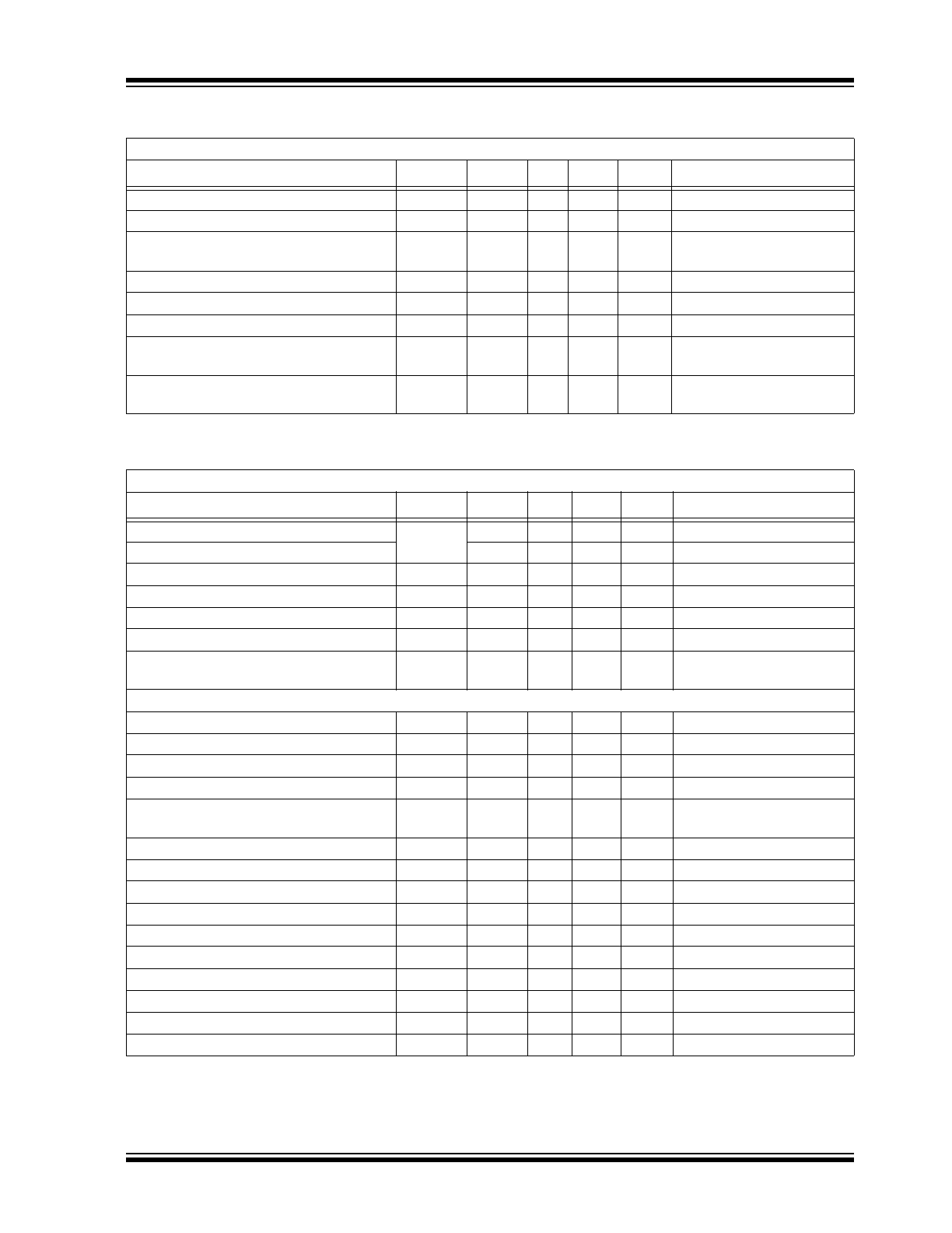
DC ELECTRICAL CHARACTERISTICS
Electrical Specifications: Over operating conditions unless otherwise noted
Parameter
Sym.
Min.
Typ. Max.
Unit
Conditions
HV
OUT
Voltage Swing
HV
OUT
0
—
V
PP
–5
V
Input Voltage Offset
V
INOS
—
—
±40
mV
Input referred
Feedback Resistance from HV
OUT
to Ground
R
FB
9.6
12
—
MΩ
HV
OUT
Capacitive Load
C
LOAD
0
—
3000
pF
HV
OUT
Sourcing Current Limiting Range
I
SOURCE
50
—
500
µA
I
SOURCE
= 12.5V/R
SOURCE
HV
OUT
Sinking Current Limiting Range
I
SINK
50
—
500
µA
I
SINK
= 12.5V/R
SINK
External Resistance Range
for Setting Maximum Current Source
R
SOURCE
25
—
250
kΩ
External Resistance Range for Setting
Maximum Current Sink
R
SINK
25
—
250
kΩ
2017 Microchip Technology Inc.
DS20005827A-page 5
HV257
AC ELECTRICAL CHARACTERISTICS
Electrical Specifications: Over operating conditions unless otherwise noted
Parameter
Sym.
Min.
Typ.
Max.
Unit
Conditions
HV
OUT
Slew Rate Rise
SR
—
2.2
—
V/µs
No load
HV
OUT
Slew Rate Fall
—
2
—
V/µs
No load
HV
OUT
–3 dB Channel Bandwidth
BW
—
4
—
kHz
V
PP
= 300V
Open-loop Gain
A
O
70
100
—
dB
Closed-loop Gain
A
V
68.4
72
75.6
V/V
DC Channel-to-channel Crosstalk
CT
DC
–80
—
—
dB
Power Supply Rejection Ratio for V
PP
,
V
DD
and V
NN
PSRR
–40
—
—
dB
SAMPLE AND HOLD
Acquisition Time
t
AQ
—
4
—
µs
Pedestal Voltage
V
PED
—
1
—
mV
Input referred
Sample-and-Hold Switch Resistance
R
SW
—
5
—
kΩ
Sample-and-Hold Capacitor
C
H
—
10
12
pF
Voltage Droop Rate During Hold Time
Relative to Input
V
DROOP
—
6
—
V/s
Output referred
Input Signal Voltage Range
V
SIG
0
—
5
V
V
SIG
Input Capacitance
C
SIG
—
33
—
pF
LOGIC DECODER
Set-up Time-address to Enable
t
SU
75
—
—
ns
Hold Time-address to Enable Bar
t
H
75
—
—
ns
Input Logic High Voltage
V
IH
2.4
—
V
DD
V
Input Logic Low Voltage
V
IL
0
—
1.2
V
Input Logic High Current
I
IH
—
—
1
µA
V
IH
= V
DD
Input Logic Low Current
I
IL
–1
—
—
µA
V
IL
= 0V
Logic Input Capacitance
C
IN
—
—
15
pF
HV257
DS20005827A-page 6
2017 Microchip Technology Inc.
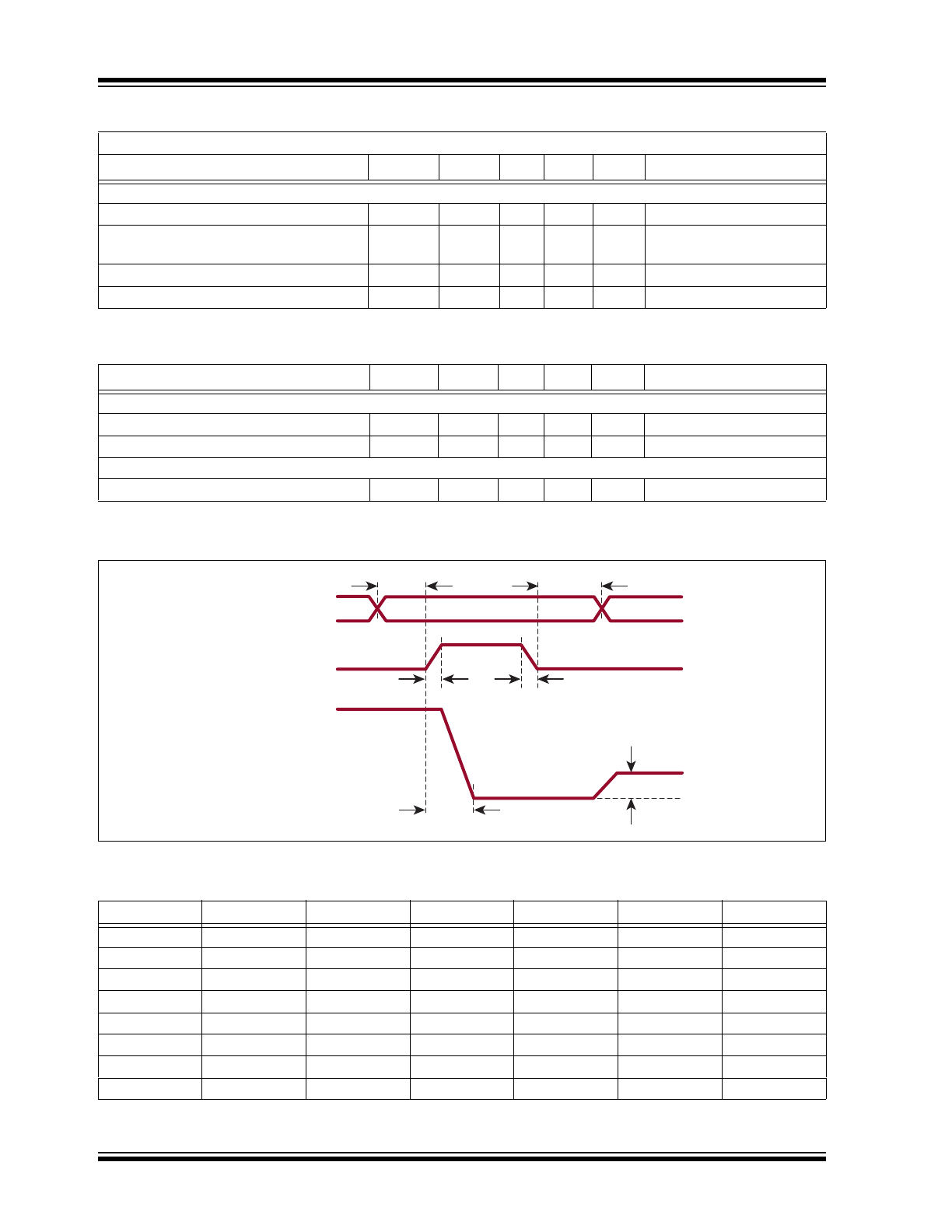
Timing Waveforms of
t
SU
t
H
Hold Step
(V
PEDESTAL
)
Hold
Hold
Sample
A0-A4
EN
HVOpamp
t
R/F
Acquisition Window
Sample-and-Hold
DECODER FUNCTION TABLE
A
4
A
3
A
2
A
1
A
0
EN
Selected S/H
L
L
L
L
L
H
0
L
L
L
L
H
H
1
L
L
L
H
L
H
2
L
L
L
H
H
H
3
↕
↕
↕
↕
↕
↕
↕
H
H
H
H
L
H
30
H
H
H
H
H
H
31
X
X
X
X
X
L
All Open
TEMPERATURE DIODE
Peak Inverse Voltage
PIV
—
—
5
V
Cathode to anode
Forward Diode Drop
V
F
—
0.6
—
V
I
F
= 100 µA, anode to cath-
ode at T
A
= 25°C
Forward Diode Current
I
F
—
—
100
µA
Anode to cathode
V
F
Temperature Coefficient
T
C
—
–2.2
—
mV/°C Anode to cathode
TEMPERATURE SPECIFICATIONS
Parameter
Sym.
Min.
Typ.
Max.
Unit
Conditions
TEMPERATURE RANGE
Maximum Junction Temperature
T
J
—
—
+150
°C
Storage Temperature
T
S
–65
—
+150
°C
PACKAGE THERMAL RESISTANCE
100-lead MQFP
JA
—
39
—
°C/W
AC ELECTRICAL CHARACTERISTICS (CONTINUED)
Electrical Specifications: Over operating conditions unless otherwise noted
Parameter
Sym.
Min.
Typ.
Max.
Unit
Conditions
2017 Microchip Technology Inc.
DS20005827A-page 7
HV257
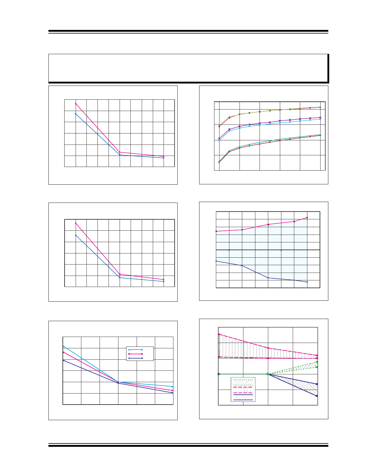
2.0
TYPICAL PERFORMANCE CURVES
(V
PP
= 300V, V
DD
= 6.5V, V
NN
= 5.5V, T
A
= 25
O
C)
R
SINK
(kΩ)
I
SINK
(μA)
600
500
400
300
200
100
0
25 150 250
min
max
Note:
The graphs and tables provided following this note are a statistical summary based on a limited number of
samples and are provided for informational purposes only. The performance characteristics listed herein
are not tested or guaranteed. In some graphs or tables, the data presented may be outside the specified
operating range (e.g. outside specified power supply range) and therefore outside the warranted range.
FIGURE 2-1:
I
SINK
vs. R
SINK
.
min
max
(V
PP
= 300V, V
DD
= 6.5V, V
NN
= 5.5V, T
A
= 25
O
C)
R
SOURCE
(kΩ)
I
SOURCE
(μA)
600
500
400
300
200
100
0
25 150 250
FIGURE 2-2:
I
SOURCE
vs. R
SOURCE
.
120
100
80
60
40
20
0
0 2.0 4.0
(”one RC” response to one volt input step) (V
PP
= 300V, V
DD
= 6.5V, V
NN
= 5.5V, T
A
= 25
O
C)
V
SIG
(V)
HV
OUT
(mV)
+85
O
C
+25
O
C
-10
O
C
FIGURE 2-3:
Acquisition Window.
FIGURE 2-4:
Temperature Diode vs.
Temperature.
700
600
500
400
300
1.0 20 40 60 80 100
Diode Biasing Current (μA)
V
f
(mV)
(V
PP
= 300V, V
DD
= 6.5V, V
NN
= 5.5V)
-10
O
C
85
O
C
25
O
C
min
max
min
max
min
max
(V
PP
= 300V, V
DD
= 6.5V, V
NN
= 5.5V, T
A
= 25
O
C)
V
SIG
Level (V)
HV
OUT
(mV)
40
20
0
-20
-40
0 1.0 2.0 3.0 4.0
FIGURE 2-5:
HV
OUT
Charge Injection vs.
V
SIG
.
HV
OUT
(V/sec)
(V
PP
= 300V, V
DD
= 6.5V, V
NN
= 5.5V)
HV
OUT
Level (V)
3.0
2.0
1.0
0
-1.0
-2.0
0 150 280
-10
O
C
85
O
C
25
O
C
FIGURE 2-6:
H
VOUT
Droop.
HV257
DS20005827A-page 8
2017 Microchip Technology Inc.
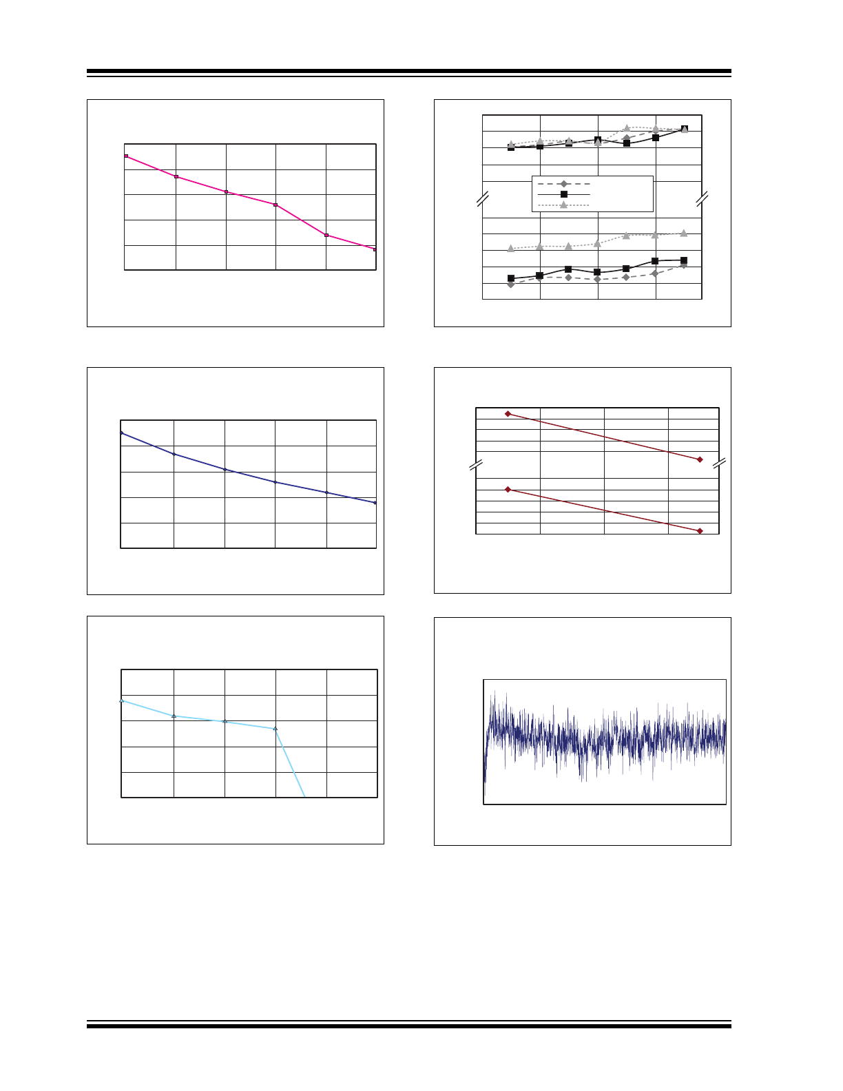
FIGURE 2-7:
Frequency (Hz)
-50
-40
-30
-20
-10
0
10 100 1k 10k 100k 1M
V
PP
PSRR (dB)
(V
PP
= 300V, V
DD
= 6.5V, V
NN
= 5.5V, T
A
= 25
O
C)
V
PP
PSRR vs. Frequency.
(V
PP
= 300V, V
DD
= 6.5V, V
NN
= 5.5V, T
A
= 25
O
C)
Frequency
V
DD
PSRR (dB)
-50
-40
-30
-20
-10
0
10 100 1k 10k 100k 1M
FIGURE 2-8:
V
DD
PSRR vs. Frequency.
Frequency
V
NN
PSRR (dB)
(V
PP
= 300V, V
DD
= 6.5V, V
NN
= 5.5V, T
A
= 25
O
C)
-50
-40
-30
-20
-10
0
10 100 1k 10k 100k 1M
FIGURE 2-9:
V
NN
PSRR vs. Frequency.
FIGURE 2-10:
3.5
3.0
2.5
2.0
1.5
-2.0
-2.5
-3.0
-3.5
-4.0
-4.5
1.0 2.0 3.0
V
IN
(Volts)
Input Offset (mV)
Offset at -10
O
C
Offset at 25
O
C
Offset at 85
O
C
(V
PP
= 300V, V
DD
= 6.5V, V
NN
= 5.5V )
Input Offset vs. V
IN
and
Temperature.
1.0 2.0 3.0
V
IN
(Volts)
Gain
(V
PP
= 300V, V
DD
= 6.5V, V
NN
= 5.5V, T
A
= -10
O
, +25
O
, +85
O
C )
73.97
73.96
73.95
73.94
73.93
72.74
72.73
72.72
72.71
72.70
72.69
FIGURE 2-11:
Gain vs. V
IN
.
HV257DFG-5037047 Q3 Dev # 3, Channel 16
(V
PP
= 300V, V
DD
= 6.5V, V
NN
= -5.0V, V
SIG
= 1.0V, T
A
= 25
O
C)
73.030
73.028
73.026
73.024
73.022
73.020
73.018
73.016
73.014
Time (hours)
0
8
HV
OUT
(V)
FIGURE 2-12:
HV
OUT
Drift.
2017 Microchip Technology Inc.
DS20005827A-page 9
HV257
3.0
PIN DESCRIPTION
The details on the pins of HV257 are listed on
Table 3-1
. Refer to
Package Type
for the location of
pins.
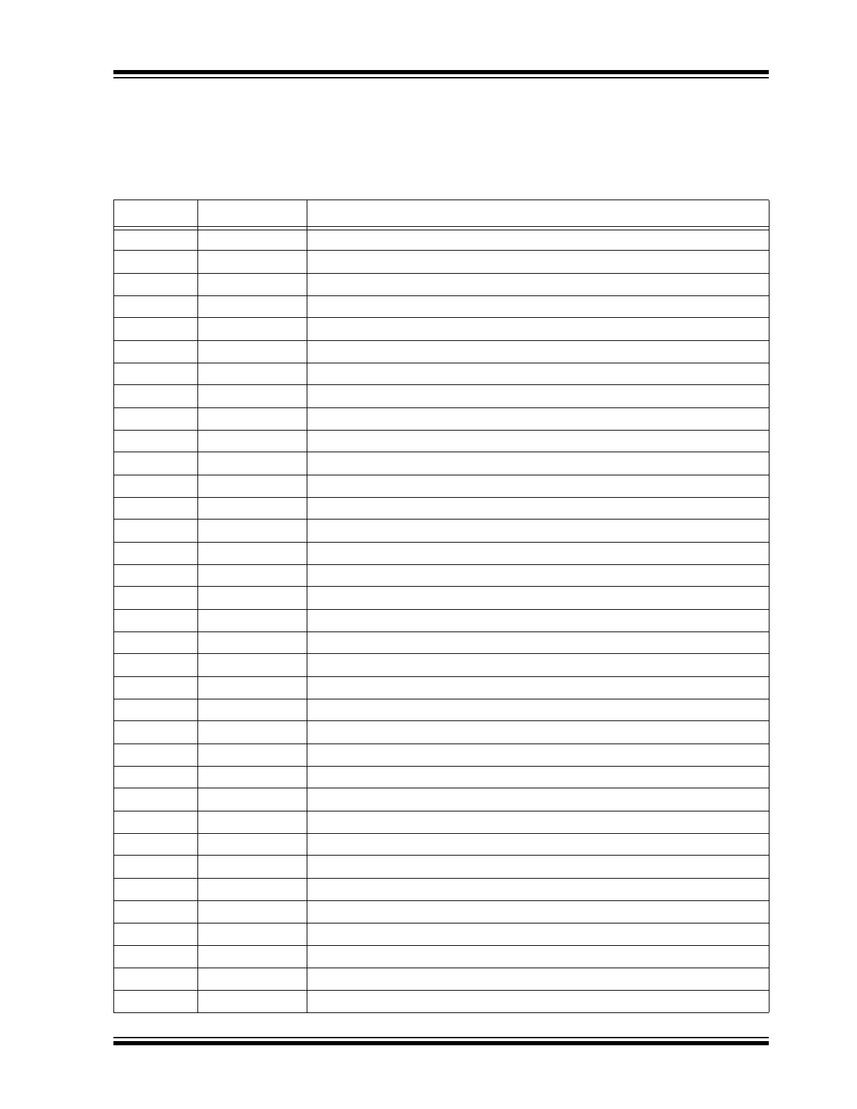
TABLE 3-1:
PIN FUNCTION TABLE
Pin Number
Pin Name
Description
1
HVOUT31
Amplifier output
2
HVOUT30
Amplifier output
3
HVOUT29
Amplifier output
4
HVOUT28
Amplifier output
5
HVOUT27
Amplifier output
6
HVOUT26
Amplifier output
7
HVOUT25
Amplifier output
8
HVOUT24
Amplifier output
9
HVOUT23
Amplifier output
10
HVOUT22
Amplifier output
11
HVOUT21
Amplifier output
12
HVOUT20
Amplifier output
13
HVOUT19
Amplifier output
14
HVOUT18
Amplifier output
15
HVOUT17
Amplifier output
16
HVOUT16
Amplifier output
17
HVOUT15
Amplifier output
18
HVOUT14
Amplifier output
19
HVOUT13
Amplifier output
20
HVOUT12
Amplifier output
21
HVOUT11
Amplifier output
22
HVOUT10
Amplifier output
23
HVOUT9
Amplifier output
24
HVOUT8
Amplifier output
25
HVOUT7
Amplifier output
26
HVOUT6
Amplifier output
27
HVOUT5
Amplifier output
28
HVOUT4
Amplifier output
29
HVOUT3
Amplifier output
30
HVOUT2
Amplifier output
31
HVOUT1
Amplifier output
32
HVOUT0
Amplifier output
33
VPP
High-voltage positive supply. There are two pads.
34
NC
No connection
35
NC
No connection

HV257
DS20005827A-page 10
2017 Microchip Technology Inc.
36
NC
No connection
37
NC
No connection
38
NC
No connection
39
AGND
Analog ground. There are three pads. They need to be externally connected.
40
AVNN
Analog low-voltage negative supply. This should be at the same potential as
DVNN. There are two pads.
41
NC
No connection
42
AVDD
Analog low-voltage positive supply. This should be at the same potential as
DVDD. There are two pads.
43
AGND
Analog ground. There are three pads. They need to be externally connected.
44
DVNN
Digital low-voltage negative supply. This should be at the same potential as
AVNN. There are two pads.
45
DVDD
Digital low-voltage positive supply. This should be at the same potential as AVDD.
There are two pads.
46
NC
No connection
47
NC
No connection
48
NC
No connection
49
NC
No connection
50
NC
No connection
51
NC
No connection
52
NC
No connection
53
NC
No connection
54
NC
No connection
55
NC
No connection
56
NC
No connection
57
NC
No connection
58
NC
No connection
59
NC
No connection
60
NC
No connection
61
NC
No connection
62
NC
No connection
63
NC
No connection
64
NC
No connection
65
NC
No connection
66
NC
No connection
67
NC
No connection
68
NC
No connection
69
NC
No connection
70
NC
No connection
71
NC
No connection
TABLE 3-1:
PIN FUNCTION TABLE (CONTINUED)
Pin Number
Pin Name
Description