
S E M I C O N D U C T O R
8-103
November 1996
HA7210, HA7211
10kHz to 10MHz, Low Power Crystal Oscillator
Features
• Single Supply Operation at 32kHz . . . . . . . . . . 2V to 7V
• Operating Frequency Range. . . . . . . . 10kHz to 10MHz
• Supply Current at 32kHz . . . . . . . . . . . . . . . . . . . . . .5
µ
A
• Supply Current at 1MHz . . . . . . . . . . . . . . . . . . . .130
µ
A
• Drives 2 CMOS Loads
• Only Requires an External Crystal for Operation
• Two Pinouts Available
Applications
• Battery Powered Circuits
• Remote Metering
• Embedded Microprocessors
• Palm Top/Notebook PC
• Related Literature
- AN9334, Improving HA7210 Start-Up Time
Description
The HA7210 and HA7211 are very low power crystal-controlled
oscillators that can be externally programmed to operate
between 10kHz and 10MHz. For normal operation it requires
only the addition of a crystal. The part exhibits very high stabil-
ity over a wide operating voltage and temperature range.
The HA7210 and HA7211 also feature a disable mode that
switches the output to a high impedance state. This feature
is useful for minimizing power dissipation during standby and
when multiple oscillator circuits are employed.
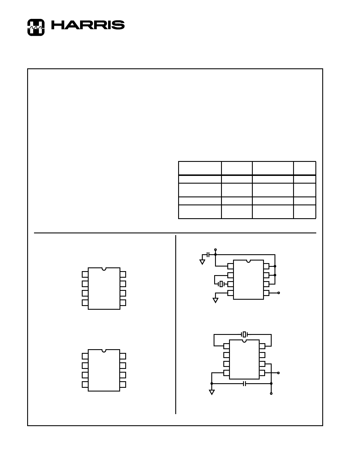
Pinouts
HA7210
(PDIP, SOIC)
TOP VIEW
HA7211
(SOIC)
TOP VIEW
Typical Application Circuits
32.768kHz MICROPOWER CLOCK OSCILLATOR
NOTE:
1. Internal pull-up resistors provided for both HA7210 and HA7211.
Ordering Information
PART NUMBER
(BRAND)
TEMP.
RANGE (
o
C)
PACKAGE
PKG.
NO.
HA7210IP
-40 to 85
8 Ld PDIP
E8.3
HA7210IB
(H7210I)
-40 to 85
8 Ld SOIC
M8.15
HA7210Y
-40 to 85
DIE
HA7211IB
(H7211I)
-40 to 85
8 Ld SOIC
M8.15
V
DD
OSC IN
OSC OUT
V
SS
1
2
3
4
8
7
6
5
ENABLE
FREQ 2
FREQ 1
OUTPUT
OSC OUT
ENABLE
FREQ 1
V
SS
1
2
3
4
8
7
6
5
OSC IN
FREQ 2
V
DD
OUTPUT
V
DD
1
2
3
4
8
7
6
5
HA7210
32.768kHz
CLOCK
32.768kHz
CRYSTAL
0.1
µ
F
1
2
3
4
8
7
6
5
32.768kHz
CLOCK
NC (NOTE 1)
0.1
µ
F
NC (NOTE 1)
V
DD
NC (NOTE 1)
32.768kHz CRYSTAL
HA7211
CAUTION: These devices are sensitive to electrostatic discharge. Users should follow proper IC Handling Procedures.
Copyright
©
Harris Corporation 1996
File Number
3389.6
8-104
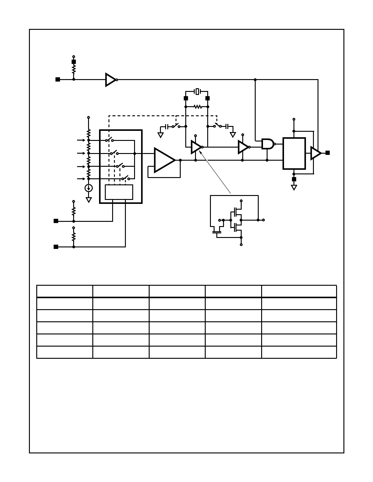
Simplified Block Diagram
(HA7210)
+
-
LEVEL
SHIFTER
BUFFER
BUFFER AMP
OSC IN 2
3 OSC OUT
EXTERNAL CRYSTAL
V
DD
V
DD
I
BIAS
V
DD
- 1.4V
V
DD
- 2.2V
V
DD
- 3.0V
V
DD
- 3.8V
FREQ 1
FREQ 2
7
6
ENABLE
8
V
DD
15pF
S
1B
S
1C
15pF
V
DD
R
F
V
DD
V
RN
V
RN
S
1A
S
2
S
3
S
4
V
DD
4
V
SS
5
OUTPUT
V
DD
1
N
P
V
DD
V
RN
P
IN
R
F
OUT
OSCILLATOR
(NOTE 2)
(NOTE 2)
(NOTE 2)
1 OF 4
DECODE
FREQUENCY SELECTION TRUTH TABLE
ENABLE
FREQ 1
FREQ 2
SWITCH
OUTPUT RANGE
1
1
1
S
1A
, S
1B
, S
1C
10kHz - 100kHz
1
1
0
S
2
100kHz - 1MHz
1
0
1
S
3
1MHz - 5MHz
1
0
0
S
4
5MHz - 10MHz+
0
X
X
X
High Impedance
NOTE:
2. Logic input pull-up resistors are constant current source of 0.4
µ
A.
HA7210, HA7211
8-105
Absolute Maximum Ratings
Thermal Information
Supply Voltage . . . . . . . . . . . . . . . . . . . . . . . . . . . . . . . . . . . . . . 10V
Voltage (any pin). . . . . . . . . . . . . . . . . . . . . . V
SS
-0.3V to V
DD
+0.3V
ESD Rating
Human Body Model (Per MIL-STD-883 Method 3015.7) . . 4000V
Operating Conditions
Temperature Range (Note 3) . . . . . . . . . . . . . . . . . . -40
o
C to 85
o
C
Thermal Resistance (Typical, Note 4)
θ
JA
(
o
C/W)
PDIP Package . . . . . . . . . . . . . . . . . . . . . . . . . . . . .
125
SOIC Package . . . . . . . . . . . . . . . . . . . . . . . . . . . . .
170
Maximum Junction Temperature (Plastic Package) . . . . . . . . 150
o
C
Maximum Storage Temperature Range . . . . . . . . . -65
o
C to 150
o
C
Maximum Lead Temperature (Soldering 10s) . . . . . . . . . . . . 300
o
C
(SOIC - Lead Tips Only)
CAUTION: Stresses above those listed in “Absolute Maximum Ratings” may cause permanent damage to the device. This is a stress only rating and operation
of the device at these or any other conditions above those indicated in the operational sections of this specification is not implied.
NOTES:
3. This product is production tested at 25
o
C only.
4.
θ
JA
is measured with the component mounted on an evaluation PC board in free air.
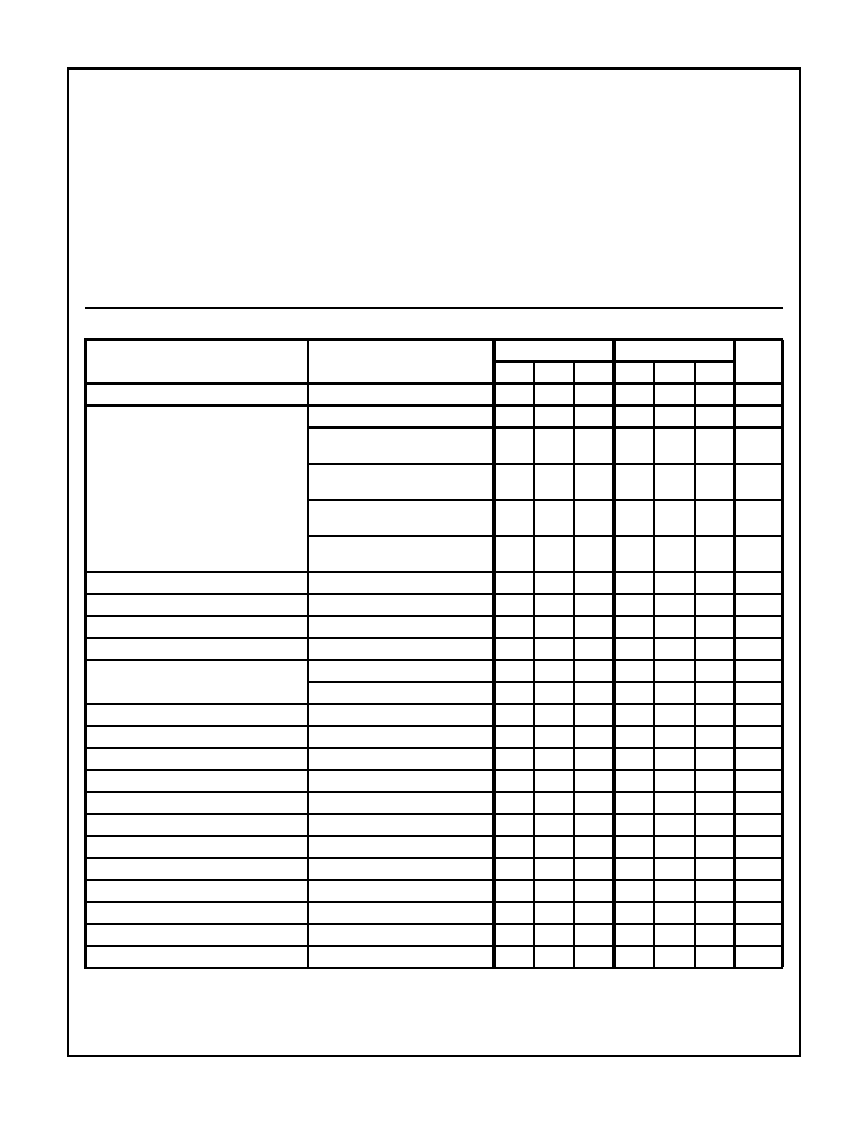
Electrical Specifications
V
SS
= GND, T
A
= 25
o
C, Unless Otherwise Specified
PARAMETER
TEST CONDITIONS
V
DD
= 5V
V
DD
= 3V
UNITS
MIN
TYP
MAX
MIN
TYP
MAX
V
DD
Supply Range
f
OSC
= 32kHz
2
5
7
-
-
-
V
I
DD
Supply Current
f
OSC
= 32kHz, EN = 0 (Standby)
-
5.0
9.0
-
-
-
µ
A
f
OSC
= 32kHz, C
L
= 10pF (Note 5),
EN = 1, Freq1 = 1, Freq2 = 1
-
5.2
10.2
-
3.6
6.1
µ
A
f
OSC
= 32kHz, C
L
= 40pF, EN = 1,
Freq1 = 1, Freq2 = 1
-
10
15
-
6.5
9
µ
A
f
OSC
= 1MHz, C
L
= 10pF (Note 5),
EN = 1, Freq1 = 0, Freq2 = 1
-
130
200
-
90
180
µ
A
f
OSC
= 1MHz, C
L
= 40pF, EN = 1,
Freq1 = 0, Freq2 = 1
-
270
350
-
180
270
µ
A
V
OH
Output High Voltage
I
OUT
= -1mA
4.0
4.9
-
-
2.8
-
V
V
OL
Output Low Voltage
I
OUT
= 1mA
-
0.07
0.4
-
0.1
-
V
I
OH
Output High Current
V
OUT
≥
4V
-
-10
-5
-
-
-
mA
I
OL
Output Low Current
V
OUT
≤
0.4V
5.0
10.0
-
-
-
-
mA
Three-State Leakage Current
V
OUT
= 0V, 5V, T
A
= 25
o
C, -40
o
C
-
0.1
-
-
-
-
nA
V
OUT
= 0V, 5V, T
A
= 85
o
C
-
10
-
-
-
-
nA
I
IN
Enable, Freq1, Freq2 Input Current
V
IN
= V
SS
to V
DD
-
0.4
1.0
-
-
-
µ
A
V
IH
Input High Voltage Enable, Freq1, Freq2
2.0
-
-
-
-
-
V
V
IL
Input Low Voltage Enable, Freq1, Freq2
-
-
0.8
-
-
-
V
Enable Time
C
L
= 18pF, R
L
= 1k
Ω
-
800
-
-
-
-
ns
Disable Time
C
L
= 18pF, R
L
= 1k
Ω
-
90
-
-
-
-
ns
t
R
Output Rise Time
10% - 90%, f
OSC
= 32kHz, C
L
= 40pF
-
12
25
-
12
-
ns
t
F
Output Fall Time
10% - 90%, f
OSC
= 32kHz, C
L
= 40pF
-
12
25
-
14
-
ns
Duty Cycle, Packaged Part Only (Note 6)
C
L
= 40pF, f
OSC
= 1MHz
40
54
60
-
-
-
%
Duty Cycle, (See Typical Curves)
C
L
= 40pF, f
OSC
= 32kHz
-
41
-
-
44
-
%
Frequency Stability vs Supply Voltage
f
OSC
= 32kHz, V
DD
= 5V, C
L
=10pF
-
1
-
-
-
-
ppm/V
Frequency Stability vs Temperature
f
OSC
= 32kHz, V
DD
= 5V, C
L
=10pF
-
0.1
-
-
-
-
ppm/
o
C
Frequency Stability vs Load
f
OSC
= 32kHz, V
DD
= 5V, C
L
=10pF
-
0.01
-
-
-
-
ppm/pF
NOTES:
5. Calculated using the equation I
DD
= I
DD
(No Load) + (V
DD
) (f
OSC
)(C
L
)
6. Duty cycle will vary with supply voltage, oscillation frequency, and parasitic capacitance on the crystal pins.
HA7210, HA7211
8-106
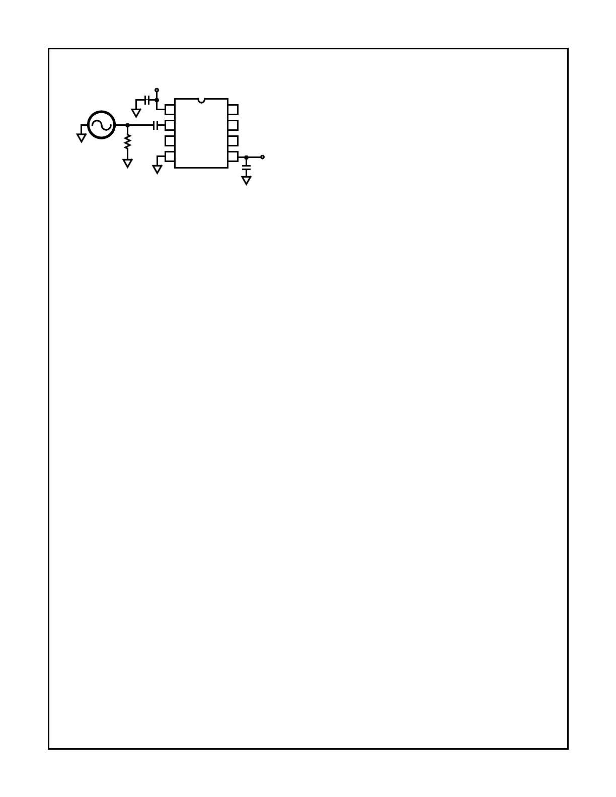
Test Circuit
In production the HA7210 is tested with a 32kHz and a
1MHz crystal. However for characterization purposes data
was taken using a sinewave generator as the frequency
determining element, as shown in Figure 1. The 1V
P-P
input
is a smaller amplitude than what a typical crystal would gen-
erate so the transitions are slower. In general the Generator
data will show a “worst case” number for I
DD
, duty cycle, and
rise/fall time. The Generator test method is useful for testing
a variety of frequencies quickly and provides curves which
can be used for understanding performance trends. Data for
the HA7210 using crystals has also been taken. This data
has been overlaid onto the generator data to provide a refer-
ence for comparison.
Application Information
Theory Of Operation
The HA7210 and HA7211 are Pierce Oscillators optimized
for low power consumption, requiring no external compo-
nents except for a bypass capacitor and a Parallel Mode
Crystal. The Simplified Block Diagram shows the Crystal
attached to pins 2 and 3, (HA7210) the Oscillator input and
output. The crystal drive circuitry is detailed showing the
simple CMOS inverter stage and the P-channel device being
used as biasing resistor R
F
. The inverter will operate mostly
in its linear region increasing the amplitude of the oscillation
until limited by its transconductance and voltage rails, V
DD
and V
RN
. The inverter is self biasing using R
F
to center the
oscillating waveform at the input threshold. Do not interfere
with this bias function with external loads or excessive leak-
age on pin 2 for HA7210, pin 8 for HA7211. Nominal value
for R
F
is 17M
Ω
in the lowest frequency range to 7M
Ω
in the
highest frequency range.
The HA7210 and HA7211 optimizes its power for 4 fre-
quency ranges selected by digital inputs Freq1 and Freq2 as
shown in the Block Diagram. Internal pull up resistors (con-
stant current 0.4
µ
A) on Enable, Freq1 and Freq2 allow the
user simply to leave one or all digital inputs not connected
for a corresponding “1” state. All digital inputs may be left
open for 10kHz to 100kHz operation.
A current source develops 4 selectable reference voltages
through series resistors. The selected voltage, V
RN
, is buff-
ered and used as the negative supply rail for the oscillator
section of the circuit. The use of a current source in the refer-
ence string allows for wide supply variation with minimal
effect on performance. The reduced operating voltage of the
oscillator section reduces power consumption and limits
transconductance and bandwidth to the frequency range
selected. For frequencies at the edge of a range, the higher
range may provide better performance.
The OSC OUT waveform on pin 3 for HA7210 (pin 1 for
HA7211) is squared up through a series of inverters to the
output drive stage. The Enable function is implemented with
a NAND gate in the inverter string, gating the signal to the
level shifter and output stage. Also during Disable the output
is set to a high impedance state useful for minimizing power
during standby and when multiple oscillators are OR’ed to a
single node.
Design Considerations
The low power CMOS transistors are designed to consume
power mostly during transitions. Keeping these transitions
short requires a good decoupling capacitor as close as pos-
sible to the supply pins 1 and 4 for HA7210, pins 4 and 6 for
HA7211. A ceramic 0.1
µ
F is recommended. Additional sup-
ply decoupling on the circuit board with 1
µ
F to 10
µ
F will fur-
ther reduce overshoot, ringing and power consumption. The
HA7210, when compared to a crystal and inverter alone, will
speed clock transition times, reducing power consumption of
all CMOS circuitry run from that clock.
Power consumption may be further reduced by minimizing the
capacitance on moving nodes. The majority of the power will
be used in the output stage driving the load. Minimizing the
load and parasitic capacitance on the output, pin 5, will play
the major role in minimizing supply current. A secondary
source of wasted supply current is parasitic or crystal load
capacitance on pins 2 and 3 for HA7210, pins 1 and 8 for
HA7211. The HA7210 is designed to work with most available
crystals in its frequency range with no external components
required. Two 15pF capacitors are internally switched onto
crystal pins 2 and 3 on the HA7210 to compensate the oscilla-
tor in the 10kHz to 100kHz frequency range.
The supply current of the HA7210 and HA7211 may be
approximately calculated from the equation:
I
DD
= I
DD
(Disabled) + V
DD
×
f
OSC
×
C
L
where:
I
DD
= Total supply current
V
DD
= Total voltage from V
DD
(pin1) to V
SS
(pin4)
f
OSC
= Frequency of Oscillation
C
L
= Output (pin5) load capacitance
Example #1:
V
DD
= 5V, f
OSC
= 100kHz, C
L
= 30pF
I
DD
(Disabled) = 4.5
µ
A (Figure 10)
I
DD
= 4.5
µ
A + (5V)(100kHz)(30pF) = 19.5
µ
A
Measured I
DD
= 20.3
µ
A
Example #2:
V
DD
= 5V, f
OSC
= 5MHz, C
L
= 30pF
I
DD
(Disabled) = 75
µ
A (Figure 9)
I
DD
= 75
µ
A + (5V)(5MHz)(30pF) = 825
µ
A
Measured I
DD
= 809
µ
A
1
2
3
4
8
7
6
5
HA7210
V
OUT
C
L
+5V
18pF
0.1
µ
F
1000pF
50
Ω
ENABLE
FREQ 2
FREQ 1
1V
P-P
FIGURE 1.
HA7210, HA7211
8-107
Crystal Selection
For general purpose applications, a Parallel Mode Crystal is
a good choice for use with the HA7210 or HA7211. However
for applications where a precision frequency is required, the
designer needs to consider other factors.
Crystals are available in two types or modes of oscillation,
Series and Parallel. Series Mode crystals are manufactured
to operate at a specified frequency with zero load capaci-
tance and appear as a near resistive impedance when oscil-
lating. Parallel Mode crystals are manufactured to operate
with a specific capacitive load in series, causing the crystal
to operate at a more inductive impedance to cancel the load
capacitor. Loading a crystal with a different capacitance will
“pull” the frequency off its value.
The HA7210 and HA7211 has 4 operating frequency ranges.
The higher three ranges do not add any loading capacitance
to the oscillator circuit. The lowest range, 10kHz to 100kHz,
automatically switches in two 15pF capacitors onto OSC IN
and OSC OUT to eliminate potential start-up problems.
These capacitors create an effective crystal loading capaci-
tor equal to the series combination of these two capacitors.
For the HA7210 and HA7211, in the lowest range, the effec-
tive loading capacitance is 7.5pF. Therefore the choice for a
crystal, in this range, should be a Parallel Mode crystal that
requires a 7.5pF load.
In the higher 3 frequency ranges, the capacitance on OSC
IN and OSC OUT will be determined by package and layout
parasitics, typically 4 to 5pF. Ideally the choice for crystal
should be a Parallel Mode set for 2.5pF load. A crystal man-
ufactured for a different load will be “pulled” from its nominal
frequency (see Crystal Pullability).
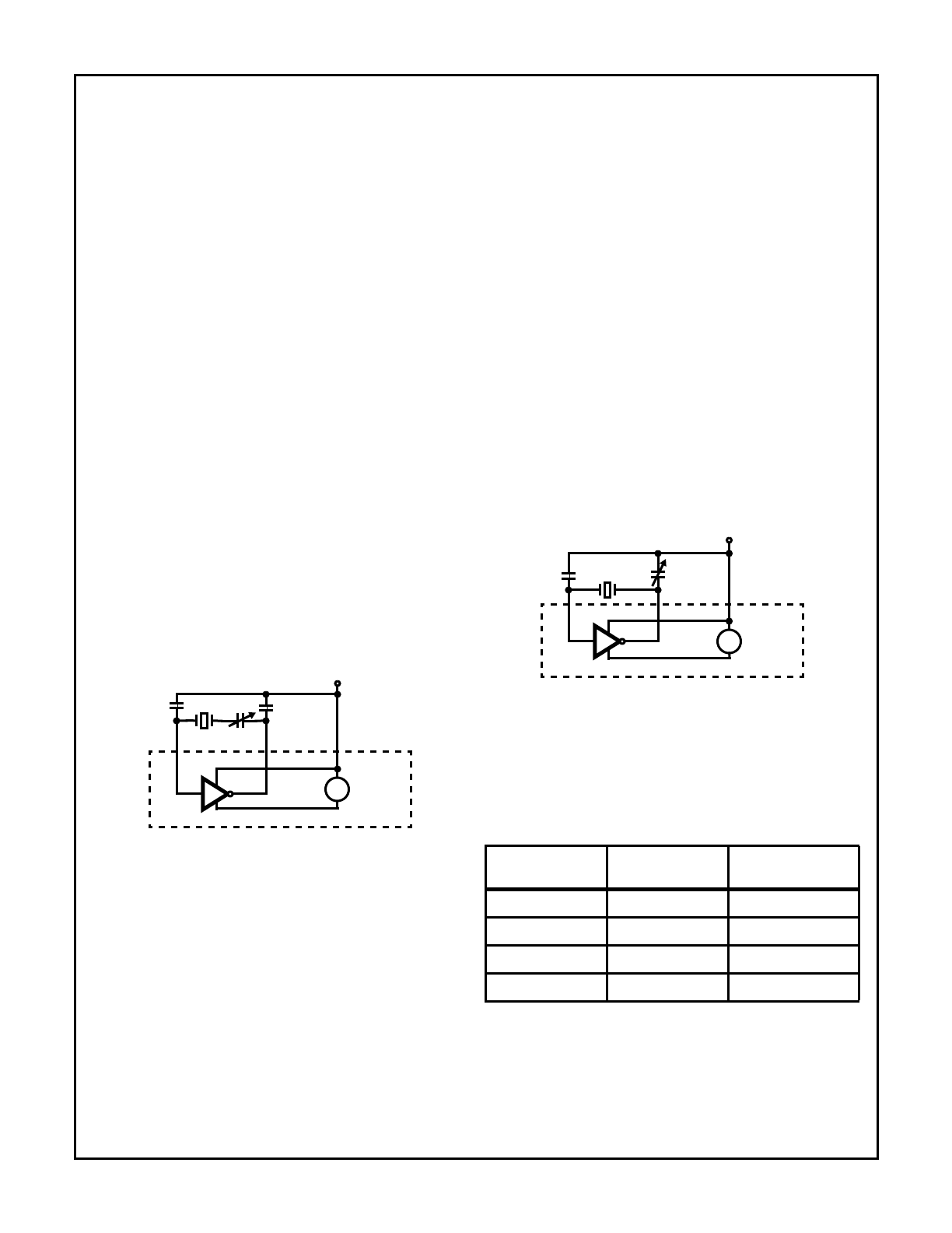
Frequency Fine Tuning
Two Methods will be discussed for fine adjustment of the
crystal frequency. The first and preferred method (Figure 2),
provides better frequency accuracy and oscillator stability
than method two (Figure 3). Method one also eliminates
start-up problems sometimes encountered with 32kHz tun-
ing fork crystals.
For best oscillator performance, two conditions must be met:
the capacitive load must be matched to both the inverter and
crystal to provide ideal conditions for oscillation, and the fre-
quency of the oscillator must be adjustable to the desired
frequency. In Method two these two goals can be at odds
with each other; either the oscillator is trimmed to frequency
by de-tuning the load circuit, or stability is increased at the
expense of absolute frequency accuracy.
Method one allows these two conditions to be met indepen-
dently. The two fixed capacitors, C
1
and C
2
, provide the opti-
mum load to the oscillator and crystal. C
3
adjusts the
frequency at which the circuit oscillates without appreciably
changing the load (and thus the stability) of the system.
Once a value for C
3
has been determined for the particular
type of crystal being used, it could be replaced with a fixed
capacitor. For the most precise control over oscillator fre-
quency, C
3
should remain adjustable.
This three capacitor tuning method will be more accurate
and stable than method two and is recommended for 32kHz
tuning fork crystals; without it they may leap into an overtone
mode when power is initially applied.
Method two has been used for many years and may be pre-
ferred in applications where cost or space is critical. Note
that in both cases the crystal loading capacitors are con-
nected between the oscillator and V
DD
; do not use V
SS
as
an AC ground. The Simplified Block Diagram shows that the
oscillating inverter does not directly connect to V
SS
but is
referenced to V
DD
and V
RN
. Therefore V
DD
is the best AC
ground available.
Typical values of the capacitors in Figure 2 are shown below.
Some trial and error may be required before the best combi-
nation is determined. The values listed are total capacitance
including parasitic or other sources. Remember that in the
10kHz to 100kHz frequency range setting the HA7210
switches in two internal 15pF capacitors.
CRYSTAL PULLABILITY
Figure 4 shows the basic equivalent circuit for a crystal and
its loading circuit.
HA7210
+5V
V
REG
C
1
C
2
XTAL
C
3
2
OSC IN
3
OSC OUT
1
V
DD
FIGURE 2.
+
-
CRYSTAL
FREQUENCY
LOAD CAPS
C
1
, C
2
TRIMMER CAP
C
3
32kHz
33pF
5pF to 50pF
1MHz
33pF
5pF to 50pF
2MHz
25pF
5pF to 50pF
4MHz
22pF
5pF to 100pF
HA7210
+
-
+5V
V
REG
C
1
C
2
XTAL
2
OSC IN
3
OSC OUT
1
V
DD
FIGURE 3.
HA7210, HA7211
8-108
Where:
C
M
= Motional Capacitance
L
M
= Motional Inductance
R
M
= Motional Resistance
C
0
= Shunt Capacitance
If loading capacitance is connected to a Series Mode Crys-
tal, the new Parallel Mode frequency of resonance may be
calculated with the following equation:
Where:
f
P
= Parallel Mode Resonant Frequency
f
S
= Series Mode Resonant Frequency
In a similar way, the Series Mode resonant frequency may
be calculated from a Parallel Mode crystal and then you may
calculate how much the frequency will “pull” with a new load.
Layout Considerations
Due to the extremely low current (and therefore high imped-
ance) the circuit board layout of the HA7210 or HA7211
must be given special attention. Stray capacitance should be
minimized. Keep the oscillator traces on a single layer of the
PCB. Avoid putting a ground plane above or below this layer.
The traces between the crystal, the capacitors, and the OSC
pins should be as short as possible. Completely surround
the oscillator components with a thick trace of V
DD
to mini-
mize coupling with any digital signals. The final assembly
must be free from contaminants such as solder flux, mois-
ture, or any other potential source of leakage. A good solder
mask will help keep the traces free of moisture and contami-
nation over time.
Further Reading
Al Little “HA7210 Low Power Oscillator: Micropower Clock
Oscillator and Op Amps Provide System Shutdown for Battery
Circuits”. Harris Semiconductor Application Note AN9317.
Robert Rood “Improving Start-Up Time at 32KHz for the
HA7210 Low Power Crystal Oscillator”. Harris Semiconductor
Application Note AN9334.
S. S. Eaton “Timekeeping Advances Through COS/MOS
Technology”. Harris Semiconductor Application Note
ICAN-6086.
E. A. Vittoz, et. al. “High-Performance Crystal Oscillator cir-
cuits: Theory and Application”. IEEE Journal of Solid-State
Circuits, Vol. 23, No3, June 1988, pp774-783.
M. A. Unkrich, et. al. “Conditions for Start-Up in Crystal
Oscillators”. IEEE Journal of Solid-State Circuits, Vol. 17,
No1, Feb. 1982, pp87-90.
Marvin E. Frerking “Crystal Oscillator Design and Tempera-
ture Compensation”. New York: Van Nostrand-Reinhold,
1978. Pierce Oscillators Discussed pp56-75.
C
1
C
2
2
OSC IN
3
OSC OUT
V
DD
C
0
C
M
L
M
R
M
FIGURE 4.
C
CL
1
1
C
1
-------
1
C
2
-------
+
--------------------------
Equivalent Crystal Load
=
=
f
P
f
S
1
C
M
2 C
0
C
CL
+
(
)
----------------------------------
+
=
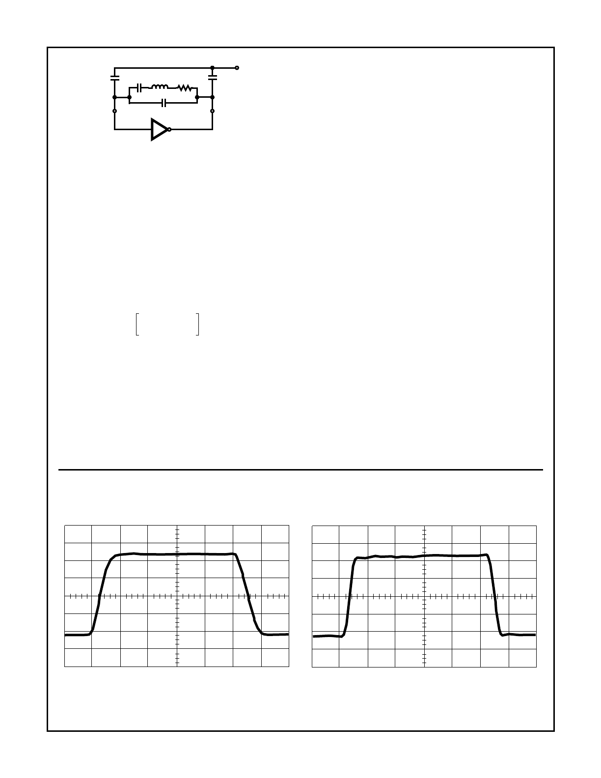
Typical Performance Curves
FIGURE 5. OUTPUT WAVEFORM (C
L
= 40pF)
FIGURE 6. OUTPUT WAVEFORM (C
L
= 18pF)
NOTE: Refer to Test Circuit (Figure 1).
1.0V/DIV.
20.0ns/DIV.
C
L
= 40pF, f
OSC
= 5MHz, V
DD
= 5V, V
SS
= GND
1.0V/DIV.
20.0ns/DIV.
C
L
= 18pF, f
OSC
= 5MHz, V
DD
= 5V, V
SS
= GND
HA7210, HA7211
8-109
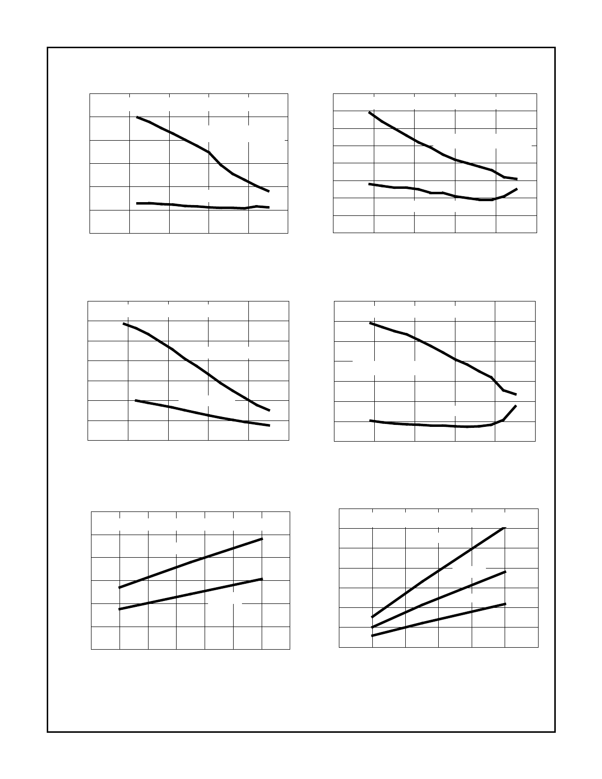
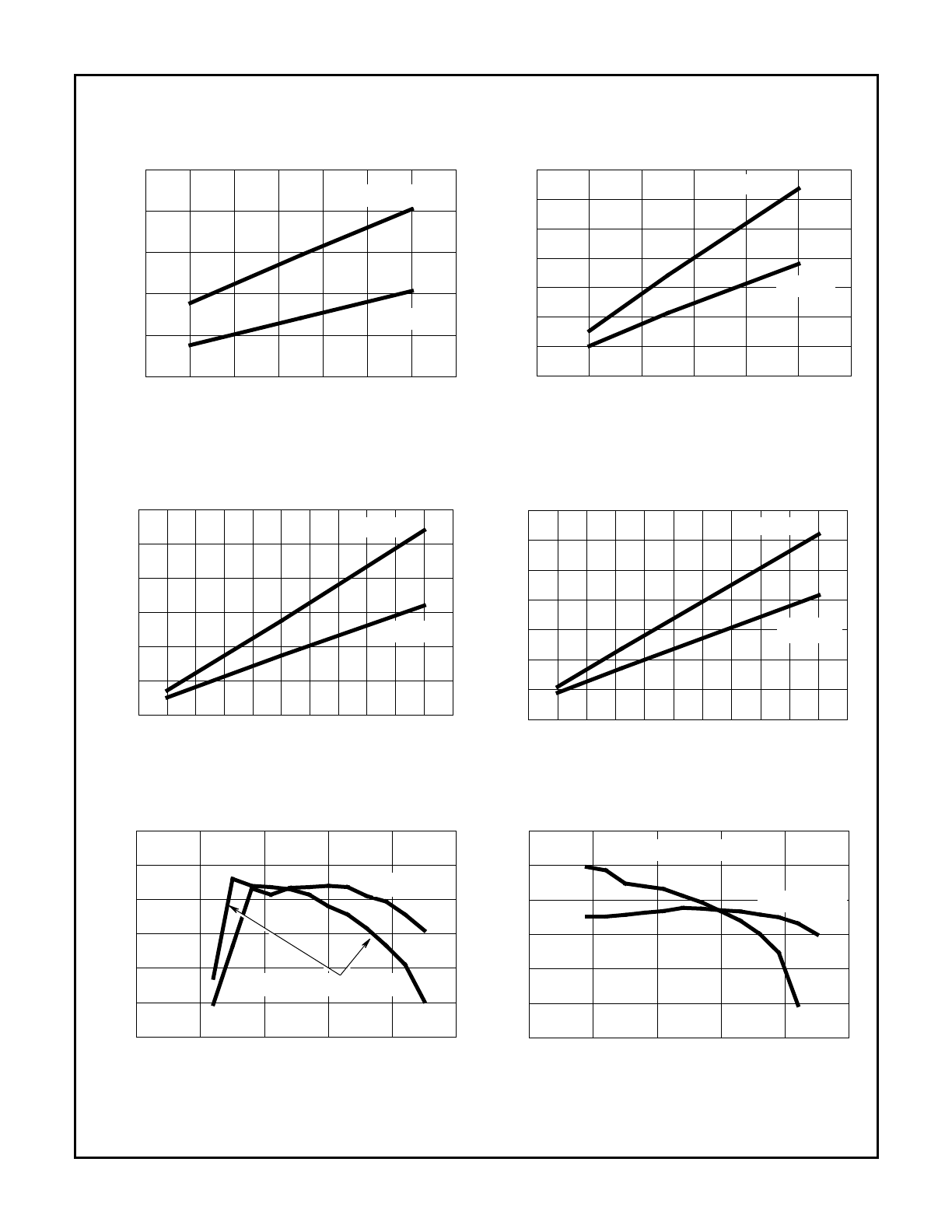
FIGURE 7. SUPPLY CURRENT vs TEMPERATURE
FIGURE 8. SUPPLY CURRENT vs TEMPERATURE
FIGURE 9. DISABLE SUPPLY CURRENT vs TEMPERATURE
FIGURE 10. DISABLE SUPPLY CURRENT vs TEMPERATURE
FIGURE 11. SUPPLY CURRENT vs FREQUENCY
FIGURE 12. SUPPLY CURRENT vs FREQUENCY
Typical Performance Curves
(Continued)
NOTE: Refer to Test Circuit (Figure 1).
-100
-50
0
50
100
150
750
800
850
900
950
1000
1050
TEMPERATURE (
o
C)
f
IN
= 5MHz, EN = 1, F1 = 0, F2 = 0, C
L
= 30pF, V
DD
= 5V
X
TAL
AT 25
o
C
SUPPL
Y CURRENT (
µ
A)
GENERATOR (1V
P-P
) (NOTE)
-100
-50
0
50
100
150
18
19
20
21
22
23
24
25
26
TEMPERATURE (
o
C)
EN = 1, F1 = 1, F2 = 1, f
IN
= 100kHz, C
L
= 30pF, V
DD
= 5V
X
TAL
AT 25
o
C
SUPPL
Y CURRENT (
µ
A)
GENERATOR (1V
P-P
) (NOTE)
-100
-50
0
50
100
150
0
50
100
150
200
250
300
350
TEMPERATURE (
o
C)
SUPPL
Y CURRENT (
µ
A)
f
IN
= 5MHz, EN = 0, F1 = 0, F2 = 0, V
DD
= 5V
GENERATOR (1V
P-P
) (NOTE)
X
TAL
AT 25
o
C
-100
-50
0
50
100
150
4
4.5
5
5.5
6
6.5
7
7.5
TEMPERATURE (
o
C)
GENERATOR (1V
P-P
) (NOTE)
X
TAL
AT 25
o
C
EN = 0, F1 = 1, F2 = 1, f
IN
= 100kHz, V
DD
= 5V
SUPPL
Y CURRENT (
µ
A)
4
5
6
7
8
9
10
11
0
500
1000
1500
2000
2500
3000
FREQUENCY (MHz)
EN = 1, F1 = 0, F2 = 0, C
L
= 18pF, GENERATOR (1V
P-P
) (NOTE)
V
DD
= +8V
V
DD
= +5V
SUPPL
Y CURRENT (
µ
A)
0
1
2
3
4
5
6
0
200
400
600
800
1000
1200
1400
FREQUENCY (MHz)
V
DD
= +8V
EN = 1, F1 = 0, F2 =1, C
L
= 18pF, GENERATOR (1V
P-P
) (NOTE)
V
DD
= +5V
V
DD
= +3V
SUPPL
Y CURRENT (
µ
A)
HA7210, HA7211
8-110
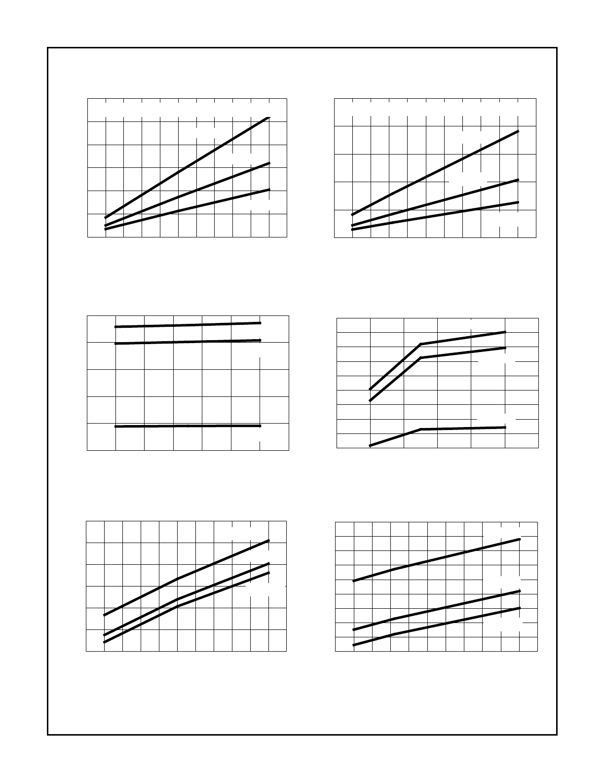
FIGURE 13. SUPPLY CURRENT vs FREQUENCY
FIGURE 14. SUPPLY CURRENT vs FREQUENCY
FIGURE 15. DISABLED SUPPLY CURRENT vs FREQUENCY
FIGURE 16. DISABLE SUPPLY CURRENT vs FREQUENCY
FIGURE 17. DISABLE SUPPLY CURRENT vs FREQUENCY
FIGURE 18. DISABLE SUPPLY CURRENT vs FREQUENCY
Typical Performance Curves
(Continued)
NOTE: Refer to Test Circuit (Figure 1).
0
100
200
300
400
500
600
700
800
900 1000 1100
0
50
100
150
200
250
300
FREQUENCY (kHz)
V
DD
= +8V
V
DD
= +5V
V
DD
= +3V
EN = 1, F1 = 0, F2 = 0, C
L
= 18pF, GENERATOR (1V
P-P
) (NOTE)
SUPPL
Y CURRENT (
µ
A)
0
10
20
30
40
50
60
70
80
90
100
110
0
10
20
30
40
50
FREQUENCY (kHz)
EN = 1, F1 = 0, F2 = 0, C
L
= 18pF, GENERATOR (1V
P-P
) (NOTE)
V
DD
= +8V
V
DD
= +5V
V
DD
= +3V
SUPPL
Y CURRENT (
µ
A)
4
5
6
7
8
9
10
11
0
50
100
150
200
250
EN = 0, F1 = 0, F2 = 0, C
L
= 18pF, GENERATOR (1V
P-P
) (NOTE)
FREQUENCY (MHz)
V
DD
= +8V
V
DD
= +5V
V
DD
= +3V
SUPPL
Y CURRENT (
µ
A)
0
1
2
3
4
5
6
30
40
50
60
70
80
90
100
110
120
EN = 0, F1 = 0, F2 = 1, C
L
= 18pF, GENERATOR (1V
P-P
) (NOTE)
FREQUENCY (MHz)
SUPPL
Y CURRENT (
µ
A)
V
DD
= +8V
V
DD
= +5V
V
DD
= +3V
0
100
200
300
400
500
600
700
800
900 1000 1100
5
10
15
20
25
30
35
EN = 0, F1 = 1, F2 = 0, C
L
= 18pF, GENERATOR (1V
P-P
) (NOTE)
FREQUENCY (kHz)
SUPPL
Y CURRENT (
µ
A)
V
DD
= +8V
V
DD
= +5V
V
DD
= +3V
0
10
20
30
40
50
60
70
80
90
100 110
2
3
4
5
6
7
8
9
10
11
EN = 0, F1 = 1, F2 = 1, C
L
= 18pF, GENERATOR (1V
P-P
) (NOTE)
FREQUENCY (kHz)
SUPPL
Y CURRENT (
µ
A)
V
DD
= +8V
V
DD
= +5V
V
DD
= +3V
HA7210, HA7211
8-111
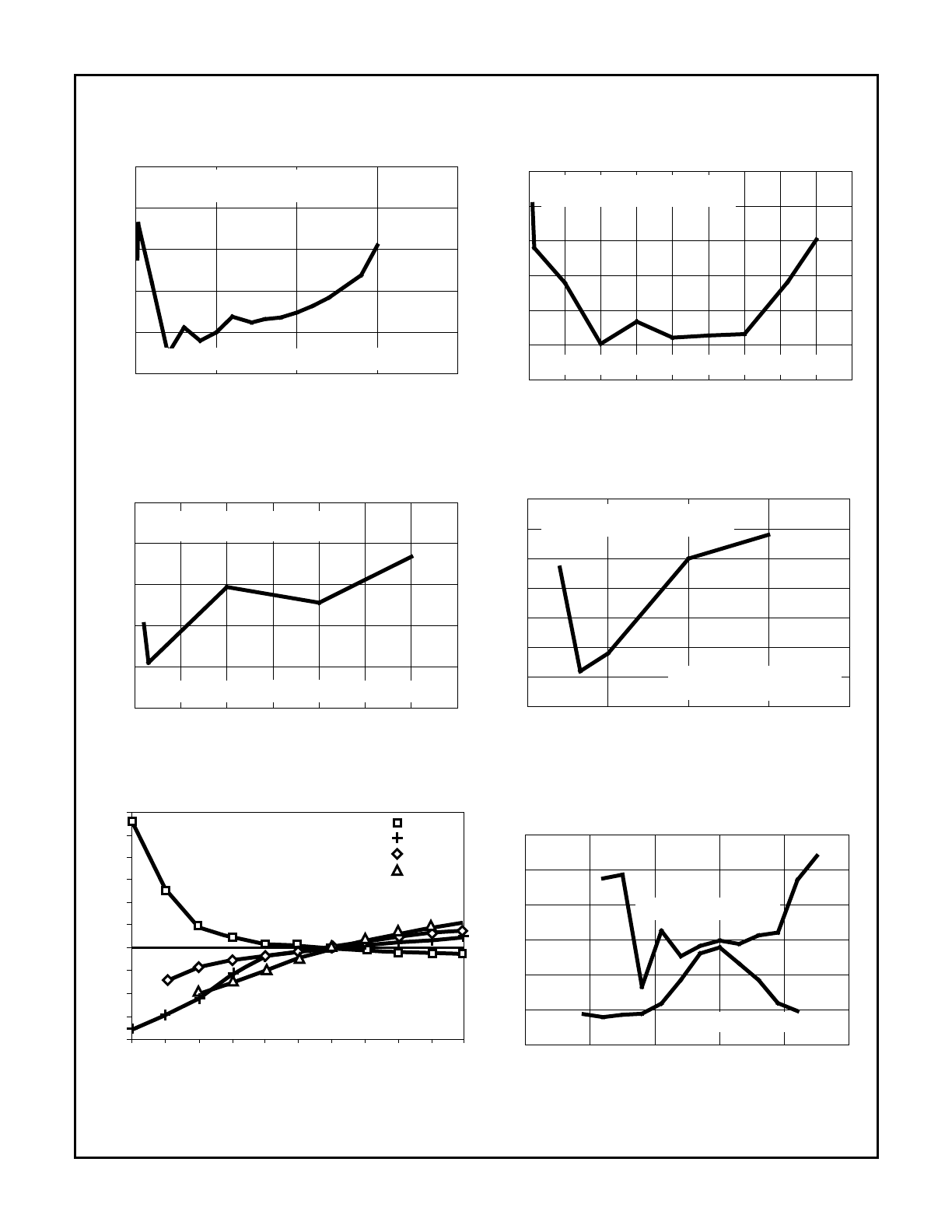
FIGURE 19. SUPPLY CURRENT vs FREQUENCY
FIGURE 20. SUPPLY CURRENT vs FREQUENCY
FIGURE 21. SUPPLY CURRENT vs FREQUENCY
FIGURE 22. SUPPLY CURRENT vs FREQUENCY
FIGURE 23. DUTY CYCLE vs TEMPERATURE
FIGURE 24. DUTY CYCLE vs TEMPERATURE
Typical Performance Curves
(Continued)
NOTE: Refer to Test Circuit (Figure 1).
4
5
6
7
8
9
10
11
500
1000
1500
2000
2500
3000
EN = 1, F1 = 0, F2 = 0, V
DD
= +5V, GENERATOR (1V
P-P
) (NOTE)
FREQUENCY (MHz)
SUPPL
Y CURRENT (
µ
A)
C
L
= 40pF
C
L
= 18pF
0
1
2
3
4
5
6
0
200
400
600
800
1000
1200
1400
EN = 1, F1 = 0, F2 = 1, V
DD
= +5V, GENERATOR (1V
P-P
) (NOTE)
FREQUENCY (MHz)
SUPPL
Y CURRENT (
µ
A)
C
L
= 40pF
C
L
= 18pF
0
100
200
300
400
500
600
700
800
900 1000 1100
0
50
100
150
200
250
300
EN = 1, F1 = 1, F2 = 0, V
DD
= +5V, GENERATOR (1V
P-P
) (NOTE)
FREQUENCY (kHz)
SUPPL
Y CURRENT (
µ
A)
C
L
= 40pF
C
L
= 18pF
0
10
20
30
40
50
60
70
80
90
100 110
0
5
10
15
20
25
30
35
EN = 1, F1 = 1, F2 = 1, V
DD
= +5V, GENERATOR (1V
P-P
) (NOTE)
FREQUENCY (kHz)
SUPPL
Y CURRENT (
µ
A)
C
L
= 18pF
C
L
= 40pF
-100
-50
0
50
100
150
30
35
40
45
50
55
60
f
IN
= 5MHz, F1 = 0, F2 = 0, C
L
= 30pF, V
DD
= 5V
TEMPERATURE (
o
C)
DUTY CYCLE (%)
X
TAL
AT 25
o
C
GENERATOR (1V
P-P
) (NOTE)
-100
-50
0
50
100
150
10
20
30
40
50
60
70
f
IN
= 100kHz, F1 = 1, F2 = 1, C
L
= 30pF, V
DD
= 5V
TEMPERATURE (
o
C)
DUTY CYCLE (%)
GENERATOR (1V
P-P
) (NOTE)
X
TAL
AT 25
o
C
HA7210, HA7211
8-112
FIGURE 25. DUTY CYCLE vs FREQUENCY
FIGURE 26. DUTY CYCLE vs FREQUENCY
FIGURE 27. DUTY CYCLE vs FREQUENCY
FIGURE 28. DUTY CYCLE vs FREQUENCY
FIGURE 29. FREQUENCY CHANGE vs V
DD
FIGURE 30. EDGE JITTER vs TEMPERATURE
Typical Performance Curves
(Continued)
NOTE: Refer to Test Circuit (Figure 1).
0
45
50
55
60
65
70
F1 = F2 = 0, V
DD
= 5V, C
L
= 18pF, C
1
= C
2
= 0
FREQUENCY (MHz)
DUTY CYCLE (%)
15
20
5
10
DATA COLLECTED USING CRYSTALS
AT EACH FREQUENCY
F1 = 0, F2 = 0 RECOMMENDED FOR 5MHz TO 10MHz RANGE
0
45
50
55
60
65
70
F1 = 0, F2 = 1, V
DD
= 5V, C
L
= 18pF, C
1
= C
2
= 0
FREQUENCY (MHz)
DUTY CYCLE (%)
7
9
4
6
1
2
3
5
8
40
DATA COLLECTED USING CRYSTALS
AT EACH FREQUENCY
F1 = 0, F2 = 1 RECOMMENDED FOR 1MHz TO 5MHz RANGE
0
40
45
50
55
60
65
F1 = 1, F2 = 0, V
DD
= 5V, C
L
= 18pF, C
1
= C
2
= 0
FREQUENCY (kHz)
DUTY CYCLE (%)
1500
2000
500
1000
2500
3000
3500
DATA COLLECTED USING CRYSTALS
AT EACH FREQUENCY
F1 = 1, F2 = 0 RECOMMENDED FOR 100kHz TO 1MHz RANGE
0
42
43
44
45
46
47
F1 = F2 = 1, V
DD
= 5V, C
L
= 18pF, C
1
= C
2
= 0
FREQUENCY (kHz)
DUTY CYCLE (%)
150
200
50
100
41
40
DATA COLLECTED USING CRYSTALS
AT EACH FREQUENCY
F1 = 1, F2 = 1 RECOMMENDED
FOR 10kHz TO 100kHz RANGE
2
4
6
-20
-10
0
5
15
20
30
V
DD
SUPPLY VOLTAGE (V)
-5
-15
25
10
32kHz
1MHz
5MHz
10MHz
FREQ
UENCY CHANGE (PPM)
DEVIATION FROM FREQUENCY AT 5.0V
-100
-50
0
50
100
150
0
1
2
3
4
5
6
V
DD
= 5V, C
L
= 30pF, GENERATOR (1V
P-P
) (NOTE)
TEMPERATURE (
o
C)
EDGE JITTER (% OF PERIOD)
f
IN
= 5MHz, F1 = 0, F2 = 0
f
IN
= 100kHz, F1 = 1, F2 = 1
HA7210, HA7211
8-113
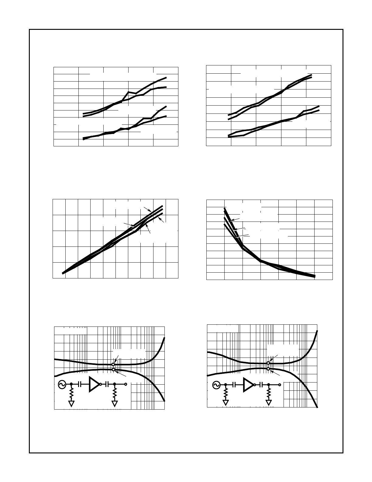
FIGURE 31. RISE/FALL TIME vs TEMPERATURE
FIGURE 32. RISE/FALL TIME vs TEMPERATURE
FIGURE 33. RISE/FALL TIME vs C
L
FIGURE 34. RISE/FALL TIME vs V
DD
FIGURE 35. TRANSCONDUCTANCE vs FREQUENCY
FIGURE 36. TRANSCONDUCTANCE vs FREQUENCY
Typical Performance Curves
(Continued)
NOTE: Refer to Test Circuit (Figure 1).
-100
-50
0
50
100
150
2
3
4
5
6
7
8
9
10
11
12
13
f
IN
= 5MHz, F1 = 0, F2 = 0, C
L
= 30pF, V
DD
= 5V
TEMPERATURE (
o
C)
t
F
GENERATOR (1V
P-P
) (NOTE)
t
R
GENERATOR (1V
P-P
) (NOTE)
t
F
X
TAL
AT 25
o
C
t
R
X
TAL
AT 25
o
C
RISE/F
ALL TIME (ns)
-100
-50
0
50
100
150
2
3
4
5
6
7
8
9
10
11
12
f
IN
= 100kHz, F1 = 1, F2 = 1, C
L
= 30pF, V
DD
= 5V
TEMPERATURE (
o
C)
t
F
GENERATOR (1V
P-P
) (NOTE)
t
R
GENERATOR (1V
P-P
) (NOTE)
t
F
X
TAL
AT 25
o
C
t
R
X
TAL
AT 25
o
C
RISE/F
ALL TIME (ns)
10
20
30
40
50
60
70
80
90
100
110
5
10
15
20
25
30
C
L
(pF)
RISE/F
ALL TIME (ns)
V
DD
= 5V, GENERATOR (1V
P-P
) (NOTE)
t
F
(f
IN
= 100kHz)
t
F
(f
IN
= 5MHz)
t
R
t
R
(f
IN
= 100kHz)
(f
IN
= 5MHz)
2
3
4
5
6
7
8
9
4
5
6
7
8
9
10
11
12
13
14
15
V
DD
(+V)
C
L
= 18pF, GENERATOR (1V
P-P
) (NOTE)
t
F
(f
IN
= 5MHz)
t
F
(f
IN
= 100kHz)
t
R
(f
IN
= 5MHz)
t
R
(f
IN
= 100kHz)
RISE/F
ALL TIME (ns)
580
540
500
460
420
380
340
300
260
10K
100K
1M
10M
140
150
160
170
180
FREQUENCY (Hz)
PHASE (DEGREES)
TRANSCONDUCT
ANCE (
µ
A/V)
V
DD
= 5V, V
SS
= GND
436.5
µ
A/V
2
3
1000pF
1
µ
F
HA7210
100
Ω
50
Ω
178
o
620
F1 = 0, F2 = 0
460
420
380
340
300
260
10K
100K
1M
10M
140
150
160
170
180
FREQUENCY (Hz)
PHASE (DEGREES)
TRANSCONDUCT
ANCE (
µ
A/V)
130
V
DD
= 5V, V
SS
= GND
311.6
µ
A/V
2
3
1000pF
1
µ
F
HA7210
100
Ω
50
Ω
500
177
o
F1 = 0, F2 = 1
HA7210, HA7211
8-114
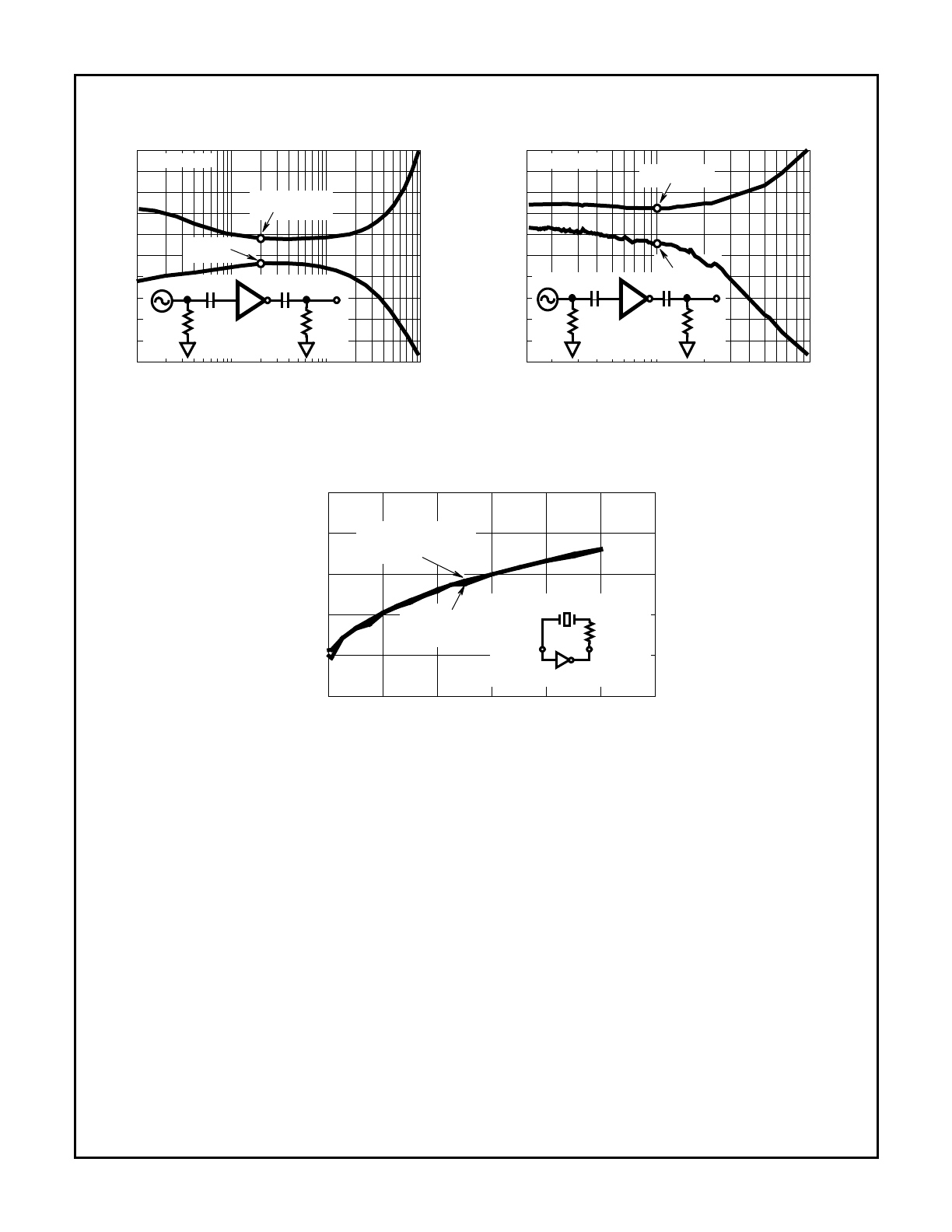
FIGURE 37. TRANSCONDUCTANCE vs FREQUENCY
FIGURE 38. TRANSCONDUCTANCE vs FREQUENCY
NOTE: Figure 39 (Duty Cycle vs R
S
at 32kHz) should only be used for 32kHz crystals. R
S
may be used at other frequencies to adjust Duty
Cycle but experimentation will be required to find an appropriate value. The R
S
value will be proportional to the effective series resis-
tance of the crystal being used.
FIGURE 39. DUTY CYCLE vs R
S
at 32kHz
Typical Performance Curves
(Continued)
NOTE: Refer to Test Circuit (Figure 1).
220
200
180
160
140
120
100
10K
100K
1M
10M
140
150
160
170
180
FREQUENCY (Hz)
PHASE (DEGREES)
TRANSCONDUCT
ANCE (
µ
A/V)
130
240
V
DD
= 5V, V
SS
= GND
156.7
µ
A/V
176.6
o
2
3
1000pF
1
µ
F
HA7210
100
Ω
50
Ω
F1 = 1, F2 = 0
15
10
5
0
10K
100K
1M
140
150
160
170
180
FREQUENCY (Hz)
PHASE (DEGREES)
TRANSCONDUCT
ANCE (
µ
A/V)
130
120
110
20
V
DD
= 5V, V
SS
= GND
6.56
µ
A/V
2
3
1000pF
1
µ
F
HA7210
100
Ω
50
Ω
166
o
F1 = 1, F2 = 1
0
20
40
60
80
100
120
35
40
45
50
55
60
F1 = F2 = 1, V
DD
= 5V, C
L
= 18pF, T
A
= 25
o
C, f
OSC
= 32.768kHz
R
S
(k
Ω
)
DUTY CYCLE (%)
NDK PART #
MX-38
EPSON PART #
C-001R32.768K-A
HA7210
XTAL
2
OSC IN
3
OSC OUT
R
S
HA7210, HA7211
8-115
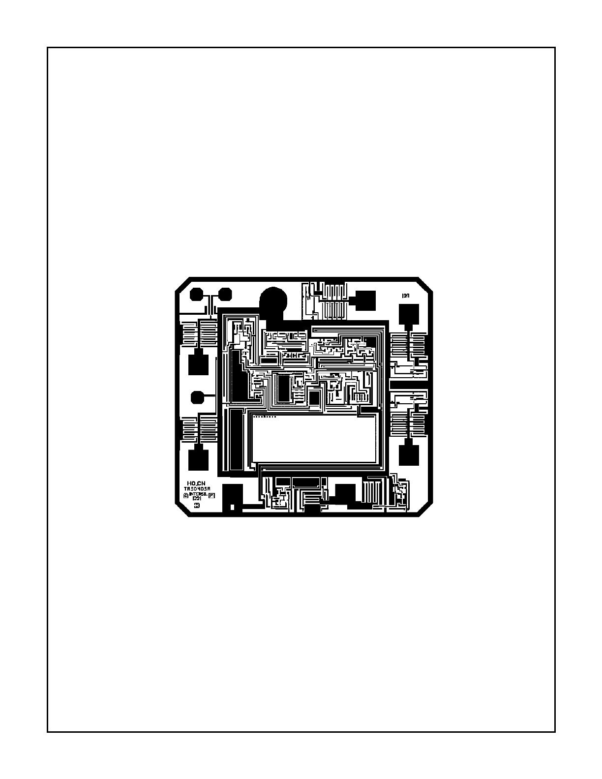
Die Characteristics
DIE DIMENSIONS:
68 mils x 64 mils x 14 mils
METALLIZATION:
Type: Si - Al
Thickness: 10k
Å
±
1k
Å
SUBSTRATE POTENTIAL
V
SS
PASSIVATION:
Type: Nitride (Si
3
N
4
) Over Silox (SiO
2
, 3% Phos)
Silox Thickness: 7k
Å
±
1k
Å
Nitride Thickness: 8k
Å
±
1k
Å
Metallization Mask Layout
HA7210
(1) V
DD
CRYSTAL (2)
CRYSTAL (3)
V
SS
(4)
OUTPUT (5)
(6) FREQ 1
(7) FREQ 2
(8) ENABLE
HA7210, HA7211