
AM26LS32AC, AM26LS33AC, AM26LS32AM, AM26LS33AM
QUADRUPLE DIFFERENTIAL LINE RECEIVERS
SLLS115C – OCTOBER 1980 – REVISED APRIL 2000
1
POST OFFICE BOX 655303
•
DALLAS, TEXAS 75265
D
AM26LS32A Meets or Exceeds the
Requirements of ANSI EIA/TIA-422-B,
EIA/TIA-423-B, and ITU Recommendations
V.10 and V.11
D
AM26LS32A Has
±
7-V Common-Mode
Range With
±
200-mV Sensitivity
D
AM26LS33A Has
±
15-V Common-Mode
Range With
±
500-mV Sensitivity
D
Input Hysteresis . . . 50 mV Typical
D
Operates From a Single 5-V Supply
D
Low-Power Schottky Circuitry
D
3-State Outputs
D
Complementary Output-Enable Inputs
D
Input Impedance . . . 12 k
Ω
Min
D
Designed to Be Interchangeable With
Advanced Micro Devices AM26LS32
and
AM26LS33
description
The AM26LS32A and AM26LS33A devices are
quadruple differential line receivers for balanced
and unbalanced digital data transmission. The
enable function is common to all four receivers
and offers a choice of active-high or active-low
input. The 3-state outputs permit connection
directly to a bus-organized system. Fail-safe
design ensures that, if the inputs are open, the
outputs are always high.
Compared to the AM26LS32 and the AM26LS33, the AM26LS32A and AM26LS33A incorporate an additional
stage of amplification to improve sensitivity. The input impedance has been increased, resulting in less loading
of the bus line. The additional stage has increased propagation delay; however, this does not affect
interchangeability in most applications.
The AM26LS32AC and AM26LS33AC are characterized for operation from 0
°
C to 70
°
C. The AM26LS32AM
and AM26LS33AM are characterized for operation over the full military temperature range of –55
°
C to 125
°
C.
Copyright
2000, Texas Instruments Incorporated
PRODUCTION DATA information is current as of publication date.
Products conform to specifications per the terms of Texas Instruments
standard warranty. Production processing does not necessarily include
testing of all parameters.
Please be aware that an important notice concerning availability, standard warranty, and use in critical applications of
Texas Instruments semiconductor products and disclaimers thereto appears at the end of this data sheet.
AM26LS32 and AM26LS33 are trademarks of Advanced Micro Devices, Inc.
1
2
3
4
5
6
7
8
16
15
14
13
12
11
10
9
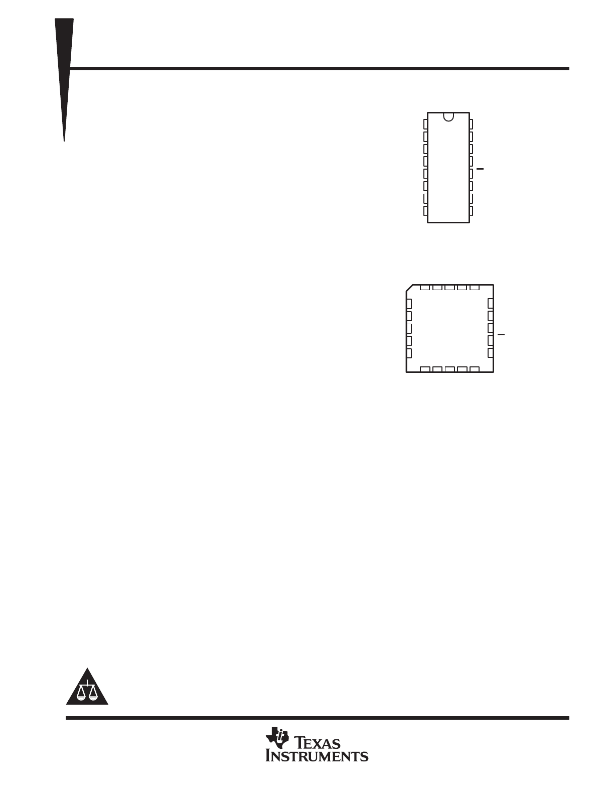
1B
1A
1Y
G
2Y
2A
2B
GND
V
CC
4B
4A
4Y
G
3Y
3A
3B
AM26LS32AC, AM26LS33AC . . . D OR N PACKAGE
AM26LS32AM, AM26LS33AM . . . J PACKAGE
(TOP VIEW)
3
2 1 20 19
9 10 11 12 13
4
5
6
7
8
18
17
16
15
14
4A
4Y
NC
G
3Y
1Y
G
NC
2Y
2A
AM26LS32AM, AM26LS33AM . . . FK PACKAGE
(TOP VIEW)
1A
1B
NC
3B
3A
4B
2B
GND
NC
V
CC
NC – No internal connection
AM26LS32AC, AM26LS33AC, AM26LS32AM, AM26LS33AM
QUADRUPLE DIFFERENTIAL LINE RECEIVERS
SLLS115C – OCTOBER 1980 – REVISED APRIL 2000
2
POST OFFICE BOX 655303
•
DALLAS, TEXAS 75265
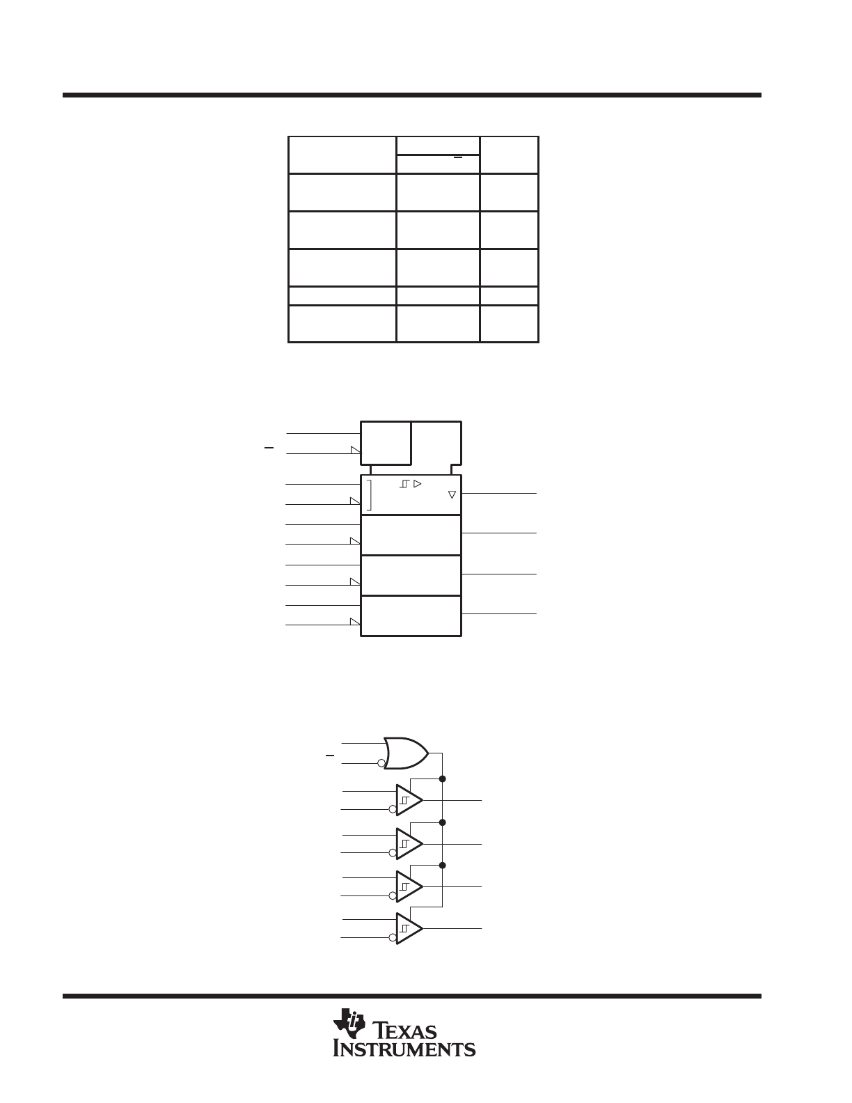
FUNCTION TABLE
(each receiver)
DIFFERENTIAL
ENABLES
OUTPUT
A – B
G
G
Y
VID
≥
VIT
H
X
H
VID
≥
VIT+
X
L
H
VIT
≤
VID
≤
VIT
H
X
?
VIT–
≤
VID
≤
VIT+
X
L
?
VID
≤
VIT
H
X
L
VID
≤
VIT–
X
L
L
X
L
H
Z
Open
H
X
H
Open
X
L
H
H = high level, L = low level, ? = indeterminate,
X = irrelevant, Z = high impedance (off)
logic symbol
†
2
1A
1
1B
1Y
3
4
G
12
≥
1
EN
6
2A
7
2B
2Y
5
10
3A
9
3B
3Y
11
14
4A
15
4B
4Y
13
G
† This symbol is in accordance with ANSI/IEEE Std 91-1984 and IEC Publication 617-12.
Pin numbers shown are for D, J, and N packages.
logic diagram (positive logic)
4
12
2
1
3
6
7
5
10
9
11
14
15
13
G
G
1A
1B
2A
2B
3A
3B
4A
4B
1Y
2Y
3Y
4Y
AM26LS32AC, AM26LS33AC, AM26LS32AM, AM26LS33AM
QUADRUPLE DIFFERENTIAL LINE RECEIVERS
SLLS115C – OCTOBER 1980 – REVISED APRIL 2000
3
POST OFFICE BOX 655303
•
DALLAS, TEXAS 75265
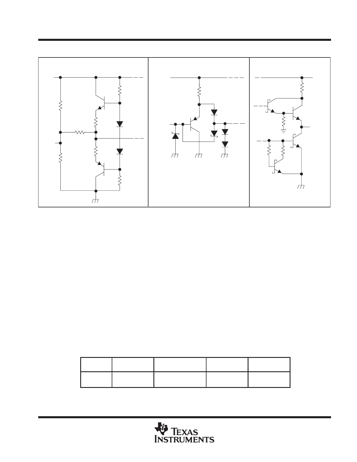
schematics of inputs and outputs
EQUIVALENT OF EACH
DIFFERENTIAL INPUT
VCC
Input
EQUIVALENT OF EACH ENABLE INPUT
Output
85
Ω
NOM
TYPICAL OF ALL OUTPUTS
8.3 k
Ω
NOM
Enable
20 k
Ω
NOM
960
Ω
NOM
960
Ω
NOM
100 k
Ω
A Input Only
VCC
100 k
Ω
B Input Only
VCC
absolute maximum ratings over operating free-air temperature range (unless otherwise noted)
†
Supply voltage, V
CC
(see Note 1)
7 V
. . . . . . . . . . . . . . . . . . . . . . . . . . . . . . . . . . . . . . . . . . . . . . . . . . . . . . . . . . . . .
Input voltage, V
I
: Any differential input
±
25 V
. . . . . . . . . . . . . . . . . . . . . . . . . . . . . . . . . . . . . . . . . . . . . . . . . . . . . . .
Other inputs
7 V
. . . . . . . . . . . . . . . . . . . . . . . . . . . . . . . . . . . . . . . . . . . . . . . . . . . . . . . . . . . . . . . .
Differential input voltage, V
ID
(see Note 2)
±
25 V
. . . . . . . . . . . . . . . . . . . . . . . . . . . . . . . . . . . . . . . . . . . . . . . . . . .
Continuous total power dissipation
See Dissipation Rating Table
. . . . . . . . . . . . . . . . . . . . . . . . . . . . . . . . . . . . .
Package thermal impedance,
θ
JA
(see Note 3): D package
73
°
C/W
. . . . . . . . . . . . . . . . . . . . . . . . . . . . . . . . . . .
N package
67
°
C/W
. . . . . . . . . . . . . . . . . . . . . . . . . . . . . . . . . . .
Lead temperature 1,6 mm (1/16 inch) from case for 10 seconds: D or N package
260
°
C
. . . . . . . . . . . . . . . .
Lead temperature 1,6 mm (1/16 inch) from case for 60 seconds: J package
300
°
C
. . . . . . . . . . . . . . . . . . . . .
Case temperature for 60 seconds, T
C
: FK package
260
°
C
. . . . . . . . . . . . . . . . . . . . . . . . . . . . . . . . . . . . . . . . . .
Storage temperature range, T
stg
–65
°
C to 150
°
C
. . . . . . . . . . . . . . . . . . . . . . . . . . . . . . . . . . . . . . . . . . . . . . . . . . .
† Stresses beyond those listed under “absolute maximum ratings” may cause permanent damage to the device. These are stress ratings only, and
functional operation of the device at these or any other conditions beyond those indicated under “recommended operating conditions” is not
implied. Exposure to absolute-maximum-rated conditions for extended periods may affect device reliability.
NOTES:
1. All voltage values, except differential voltages, are with respect to the network ground terminal.
2. Differential voltage values are at the noninverting (A) input terminals with respect to the inverting (B) input terminals.
3. The package thermal impedance is calculated in accordance with JESD 51.
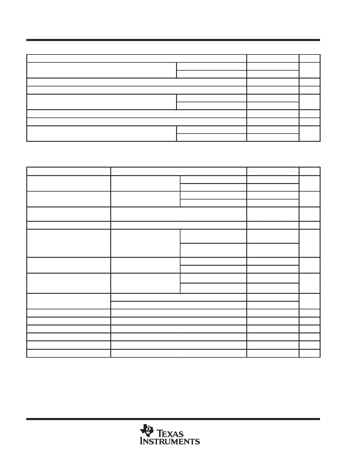
DISSIPATION RATING TABLE
PACKAGE
TA
≤
25
°
C
POWER RATING
DERATING FACTOR
ABOVE TA = 25
°
C
TA = 70
°
C
POWER RATING
TA = 125
°
C
POWER RATING
FK
1375 mW
11.0 mW/
°
C
880 mW
275 mW
J
1375 mW
11.0 mW/
°
C
880 mW
275 mW
AM26LS32AC, AM26LS33AC, AM26LS32AM, AM26LS33AM
QUADRUPLE DIFFERENTIAL LINE RECEIVERS
SLLS115C – OCTOBER 1980 – REVISED APRIL 2000
4
POST OFFICE BOX 655303
•
DALLAS, TEXAS 75265
recommended operating conditions
MIN
NOM
MAX
UNIT
Supply voltage VCC
AM26LS32AC, AM26LS33AC
4.75
5
5.25
V
Supply voltage, VCC
AM26LS32AM, AM26LS33AM
4.5
5
5.5
V
High-level input voltage, VIH
2
V
Low-level input voltage, VIL
0.8
V
Common mode input voltage VIC
AM26LS32AC, AM26LS32AM
±
7
V
Common-mode input voltage, VIC
AM26LS33AC, AM26LS33AM
±
15
V
High-level output current, IOH
–440
µ
A
Low-level output current, IOL
8
mA
Operating free air temperature TA
AM26LS32AC, AM26LS33AC
0
70
°
C
Operating free-air temperature, TA
AM26LS32AM, AM26LS33AM
–55
125
°
C
electrical characteristics over recommended ranges of V
CC
, V
IC
, and operating free-air
temperature (unless otherwise noted)
PARAMETER
TEST CONDITIONS
MIN
TYP†
MAX
UNIT
VIT
Positive-going
VO = VOHmin IOH = 440
µ
A
AM26LS32A
0.2
V
VIT+
g
g
input threshhold voltage
VO = VOHmin, IOH = –440
µ
A
AM26LS33A
0.5
V
VIT
Negative-going
VO = 0 45 V IOL = 8 mA
AM26LS32A
–0.2‡
V
VIT–
g
g
g
input threshhold voltage
VO = 0.45 V, IOL = 8 mA
AM26LS33A
–0.5‡
V
Vhys
Hysteresis voltage
(VIT+ – VIT–)
50
mV
VIK
Enable input clamp voltage
VCC = MIN,
II = –18 mA
–1.5
V
VOH
High level output voltage
VCC =MIN, VID = 1 V,
AM26LS32AC
AM26LS33AC
2.7
V
VOH
High-level output voltage
CC
,
ID
,
VI(G) = 0.8 V, IOH = –440
µ
A
AM26LS32AM
AM26LS33AM
2.5
V
VOL
Low level output voltage
VCC = MIN, VID = –1 V,
IOL = 4 mA
0.4
V
VOL
Low-level output voltage
CC
,
ID
,
VI(G) = 0.8 V
IOL = 8 mA
0.45
V
IOZ
Off-state
(high impedance state)
VCC = MAX
VO = 2.4 V
20
µ
A
IOZ
(high-impedance state)
output current
VCC = MAX
VO = 0.4 V
–20
µ
A
II
Line input current
VI = 15 V,
Other input at –10 V to 15 V
1.2
mA
II
Line input current
VI = –15 V,
Other input at –15 V to 10 V
–1.7
mA
II(EN)
Enable input current
VI = 5.5 V
100
µ
A
IIH
High-level enable current
VI = 2.7 V
20
µ
A
IIL
Low-level enable current
VI = 0.4 V
–0.36
mA
rI
Input resistance
VIC = –15 V to 15 V,
One input to ac ground
12
15
k
Ω
IOS
Short-circuit output current§
VCC = MAX
–15
–85
mA
ICC
Supply current
VCC = MAX,
All outputs disabled
52
70
mA
† All typical values are at VCC = 5 V, TA = 25
°
C, and VIC = 0.
‡ The algebraic convention, in which the less positive (more negative) limit is designated as minimum, is used in this data sheet for threshold levels
only.
§ Not more than one output should be shorted to ground at a time, and duration of the short circuit should not exceed one second.
AM26LS32AC, AM26LS33AC, AM26LS32AM, AM26LS33AM
QUADRUPLE DIFFERENTIAL LINE RECEIVERS
SLLS115C – OCTOBER 1980 – REVISED APRIL 2000
5
POST OFFICE BOX 655303
•
DALLAS, TEXAS 75265
switching characteristics, V
CC
= 5 V, T
A
= 25
°
C
PARAMETER
TEST CONDITIONS
MIN
TYP
MAX
UNIT
tPLH
Propagation delay time, low-to-high-level output
CL = 15 pF
See Figure 1
20
35
ns
tPHL
Propagation delay time, high-to-low-level output
CL = 15 pF,
See Figure 1
22
35
ns
tPZH
Output enable time to high level
CL = 15 pF
See Figure 1
17
22
ns
tPZL
Output enable time to low level
CL = 15 pF,
See Figure 1
20
25
ns
tPHZ
Output disable time from high level
CL = 5 pF
See Figure 1
21
30
ns
tPLZ
Output disable time from low level
CL = 5 pF,
See Figure 1
30
40
ns
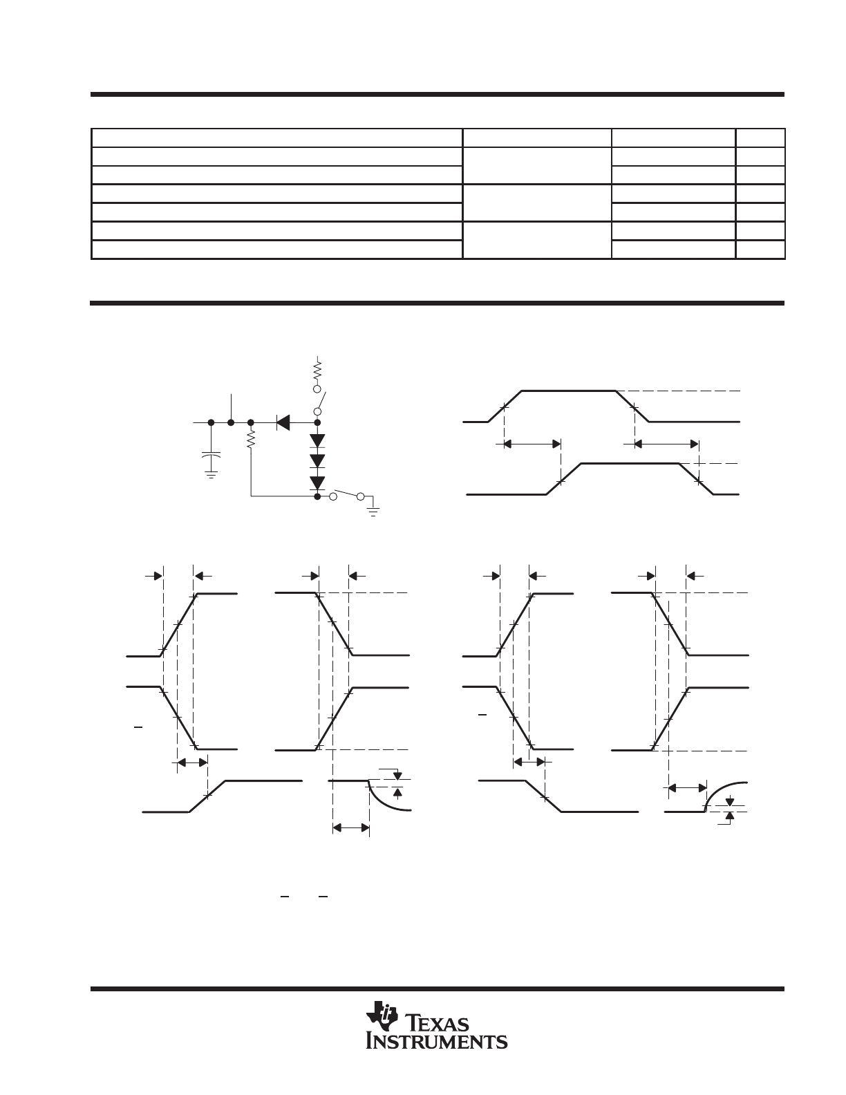
PARAMETER MEASUREMENT INFORMATION
S1 Open
S2 Closed
5 k
Ω
S1
RL = 2 k
Ω
VCC
From Output
Under Test
CL
(see Note A)
See Note B
S2
tPHL
VOH
VOL
2.5 V
–2.5 V
tPLH
S1 and S2 Closed
VOLTAGE WAVEFORMS FOR tPLH, tPHL
TEST CIRCUIT
10%
90%
10%
90%
0
3 V
10%
10%
90%
90%
1.3 V
1.3 V
1.3 V
1.3 V
3 V
0
≤
5 ns
10%
90%
10%
90%
0
3 V
10%
10%
90%
90%
1.3 V
1.3 V
1.3 V
1.3 V
3 V
0
Enable G
Enable G
tPZH
1.3 V
Output
VOH
0.5 V
≈
1.4 V
tPHZ
S1 Closed
S2 Closed
tPZL
1.3 V
S1 Closed
S2 Open
S1 Closed
S2 Closed
VOL
0.5 V
tPLZ
VOLTAGE WAVEFORMS FOR tPHZ, tPZH
VOLTAGE WAVEFORMS FOR tPLZ, tPZL
Test
Point
Output
See Note C
See Note C
Input
Output
Enable G
Enable G
≤
5 ns
≤
5 ns
≤
5 ns
≈
1.4 V
NOTES: A. CL includes probe and jig capacitance.
B. All diodes are 1N3064 or equivalent.
C. Enable G is tested with G high; G is tested with G low.
0
0
1.3 V
1.3 V
Figure 1
AM26LS32AC, AM26LS33AC, AM26LS32AM, AM26LS33AM
QUADRUPLE DIFFERENTIAL LINE RECEIVERS
SLLS115C – OCTOBER 1980 – REVISED APRIL 2000
6
POST OFFICE BOX 655303
•
DALLAS, TEXAS 75265
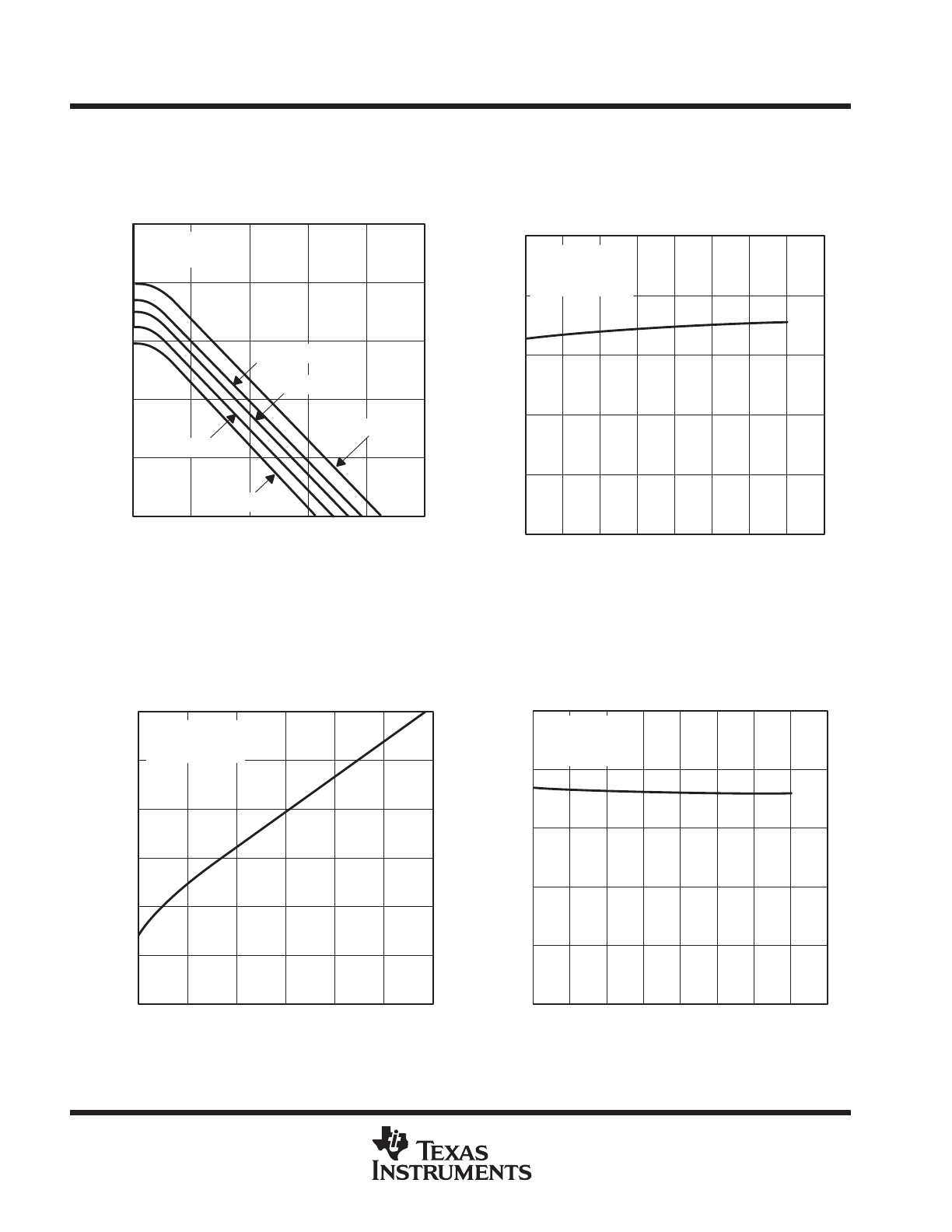
TYPICAL CHARACTERISTICS
2
1
0
0
–10
–20
–30
– High-Level Output V
oltage – V
3
4
HIGH-LEVEL OUTPUT VOLTAGE
vs
HIGH-LEVEL OUTPUT CURRENT
†
5
–40
–50
VCC = 5.25 V
VCC = 5 V
VCC = 4.75 V
IOH – High-Level Output Current – mA
V
OH
VID = 0.2 V
TA = 25
°
C
VCC = 5.5 V
VCC = 4.5 V
† VCC = 5.5 V and VCC = 4.5 V applies to M-suffix devices only.
Figure 2
2
0
0
10
20
30
40
50
60
HIGH-LEVEL OUTPUT VOLTAGE
vs
FREE-AIR TEMPERATURE
5
70
80
4
3
1
– High-Level Output V
oltage – V
V
OH
TA – Free-Air Temperature –
°
C
VCC = 5 V
VID = 0.2 mV
IOH = – 440
µ
A
Figure 3
Figure 4
0.3
0.2
0.1
0
0
5
10
– Low-Level Output V
oltage – V
0.4
0.5
LOW-LEVEL OUTPUT VOLTAGE
vs
LOW-LEVEL OUTPUT CURRENT
0.6
15
20
25
30
IOL – Low-Level Output Current – mA
V
OL
VCC = 5 V
TA = 25
°
C
VID = – 0.2 mV
Figure 5
0.3
0.2
0.1
0
0
10
20
30
40
50
0.4
0.5
LOW-LEVEL OUTPUT VOLTAGE
vs
FREE-AIR TEMPERATURE
60
70
80
– Low-Level Output V
oltage – V
V
OL
TA – Free-Air Temperature –
°
C
VCC = 5 V
VID = –0.2 V
IOL = 8 mA
AM26LS32AC, AM26LS33AC, AM26LS32AM, AM26LS33AM
QUADRUPLE DIFFERENTIAL LINE RECEIVERS
SLLS115C – OCTOBER 1980 – REVISED APRIL 2000
7
POST OFFICE BOX 655303
•
DALLAS, TEXAS 75265
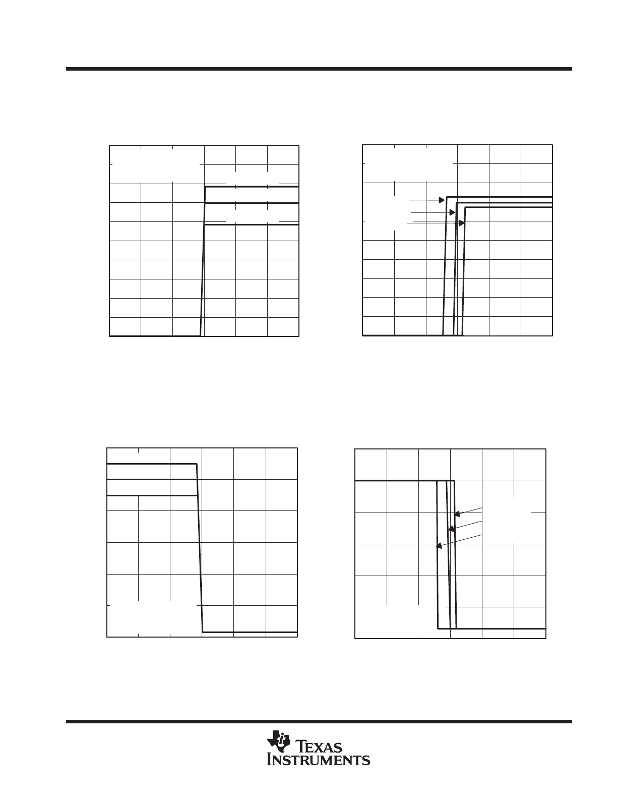
TYPICAL CHARACTERISTICS
OUTPUT VOLTAGE
vs
ENABLE G VOLTAGE
Enable G Voltage – V
3
2
0
0.5
1
1.5
4
5
2
2.5
3
1
0
– Output V
oltage – V
V
O
VID = 0.2 V
TA = 25
°
C
Load = 8 k
Ω
to GND
VCC = 5.5 V
VCC = 5 V
VCC = 4.5 V
4.5
3.5
2.5
1.5
0.5
Figure 6
OUTPUT VOLTAGE
vs
ENABLE G VOLTAGE
Enable G Voltage – V
– Output V
oltage – V
V
O
2
0
0
0.5
1
1.5
2
3
4
2.5
3
1
TA = 70
°
C
TA = 25
°
C
TA = 0
°
C
3.5
2.5
1.5
0.5
5
4.5
VCC = 5 V
VID = 0.2 V
Load = 8 k
Ω
to GND
Figure 7
Figure 8
Enable G Voltage – V
– Output V
oltage – V
V
O
3
2
1
0
0
0.5
1
4
5
6
1.5
2
2.5
3
VCC = 5.5 V
VCC = 5 V
VCC = 4.5 V
VID = –0.2 V
Load = 1 k
Ω
to VCC
TA = 25
°
C
OUTPUT VOLTAGE
vs
ENABLE G VOLTAGE
Figure 9
OUTPUT VOLTAGE
vs
ENABLE G VOLTAGE
Enable G Voltage – V
– Output V
oltage – V
V
O
3
2
1
0
0
0.5
1
4
5
6
1.5
2
2.5
3
VCC = 5 V
VID = –0.2 V
Load = 1 k
Ω
to VCC
TA = 0
°
C
TA = 25
°
C
TA = 70
°
C
AM26LS32AC, AM26LS33AC, AM26LS32AM, AM26LS33AM
QUADRUPLE DIFFERENTIAL LINE RECEIVERS
SLLS115C – OCTOBER 1980 – REVISED APRIL 2000
8
POST OFFICE BOX 655303
•
DALLAS, TEXAS 75265
TYPICAL CHARACTERISTICS
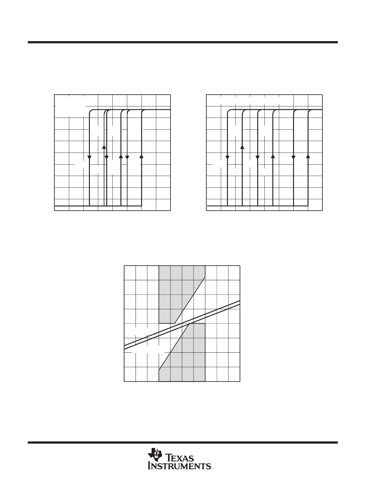
Figure 10
2.5
2
1
0.5
0
4.5
1.5
–200 –150 –100
–50
0
3.5
3
4
AM26LS32A
OUTPUT VOLTAGE
vs
DIFFERENTIAL INPUT VOLTAGE
5
50
100
150
200
VID – Differential Input Voltage – mV
– Output V
oltage – V
V
O
VCC = 5 V
IO = 0
TA = 25
°
C
VIT–
VIT+
VIC =
–7 V
VIC =
0
VIC =
7 V
VIT–
VIT+
VIT–
VIT+
2.5
2
1
0.5
0
4.5
1.5
–200 –150 –100
–50
0
3.5
3
4
AM26LS33A
OUTPUT VOLTAGE
vs
DIFFERENTIAL INPUT VOLTAGE
5
50
100
150
200
VID – Differential Input Voltage – mV
– Output V
oltage – V
V
O
VCC = 5 V, IO = 0, TA = 25
°
C
VIT–
VIT+
VIC =
–15 V
VIC =
0
VIC =
15 V
VIT–
VIT+
VIT–
VIT+
Figure 11
0
–1
–3
–4
–25 –20 –15
–5
0
5
10
– Input Current – mA
1
3
INPUT CURRENT
vs
INPUT VOLTAGE
4
20
15
–2
2
I
I
VI – Input Voltage – V
The Unshaded Area
Shows Requirements of
Paragraph 4.2.1 of ANSI
Standards EIA/TIA-422-B and
EIA/TIA-423-B.
–10
25
VCC = 5 V
VCC = 0
Figure 12
AM26LS32AC, AM26LS33AC, AM26LS32AM, AM26LS33AM
QUADRUPLE DIFFERENTIAL LINE RECEIVERS
SLLS115C – OCTOBER 1980 – REVISED APRIL 2000
9
POST OFFICE BOX 655303
•
DALLAS, TEXAS 75265
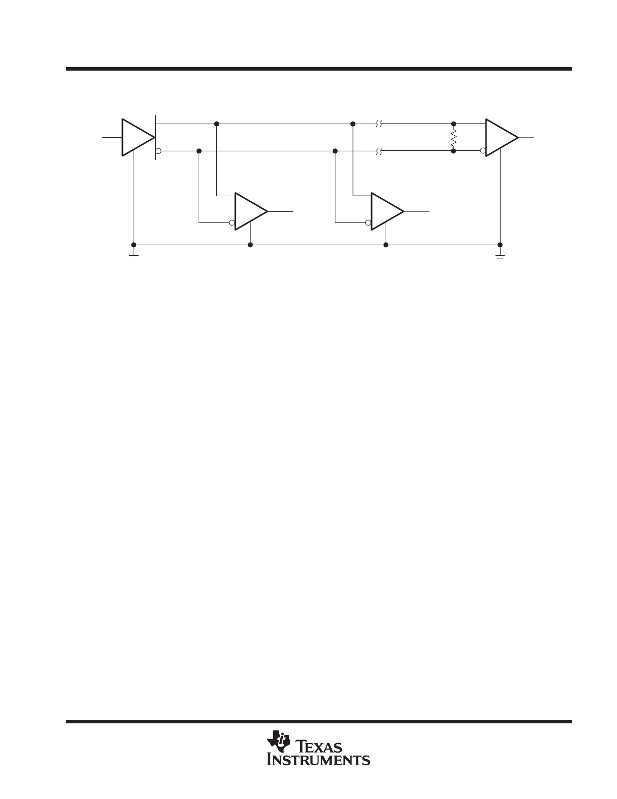
APPLICATION INFORMATION
1/4 AM26LS32AC
1/4 AM26LS31AC
Data
In
Data
Out
Data
Out
Data
Out
1/4 AM26LS32AC
1/4 AM26LS33AC
RT†
† RT equals the characteristic impedance of the line.
Figure 13. Circuit With Multiple Receivers

IMPORTANT NOTICE
Texas Instruments and its subsidiaries (TI) reserve the right to make changes to their products or to discontinue
any product or service without notice, and advise customers to obtain the latest version of relevant information
to verify, before placing orders, that information being relied on is current and complete. All products are sold
subject to the terms and conditions of sale supplied at the time of order acknowledgment, including those
pertaining to warranty, patent infringement, and limitation of liability.
TI warrants performance of its semiconductor products to the specifications applicable at the time of sale in
accordance with TI’s standard warranty. Testing and other quality control techniques are utilized to the extent
TI deems necessary to support this warranty. Specific testing of all parameters of each device is not necessarily
performed, except those mandated by government requirements.
Customers are responsible for their applications using TI components.
In order to minimize risks associated with the customer’s applications, adequate design and operating
safeguards must be provided by the customer to minimize inherent or procedural hazards.
TI assumes no liability for applications assistance or customer product design. TI does not warrant or represent
that any license, either express or implied, is granted under any patent right, copyright, mask work right, or other
intellectual property right of TI covering or relating to any combination, machine, or process in which such
semiconductor products or services might be or are used. TI’s publication of information regarding any third
party’s products or services does not constitute TI’s approval, warranty or endorsement thereof.
Copyright
2000, Texas Instruments Incorporated