
TLC5620C, TLC5620I
QUADRUPLE 8-BIT DIGITAL-TO-ANALOG CONVERTERS
SLAS081E – NOVEMBER 1994 – REVISED NOVEMBER 2001
1
POST OFFICE BOX 655303
•
DALLAS, TEXAS 75265
D
Four 8-Bit Voltage Output DACs
D
5-V Single-Supply Operation
D
Serial Interface
D
High-Impedance Reference Inputs
D
Programmable 1 or 2 Times Output Range
D
Simultaneous Update Facility
D
Internal Power-On Reset
D
Low-Power Consumption
D
Half-Buffered Output
applications
D
Programmable Voltage Sources
D
Digitally Controlled Amplifiers/Attenuators
D
Mobile Communications
D
Automatic Test Equipment
D
Process Monitoring and Control
D
Signal Synthesis
description
The TLC5620C and TLC5620I are quadruple 8-bit voltage output digital-to-analog converters (DACs) with
buffered reference inputs (high impedance). The DACs produce an output voltage that ranges between either
one or two times the reference voltages and GND, and the DACs are monotonic. The device is simple to use,
running from a single supply of 5 V. A power-on reset function is incorporated to ensure repeatable start-up
conditions.
Digital control of the TLC5620C and TLC5620I are over a simple three-wire serial bus that is CMOS compatible
and easily interfaced to all popular microprocessor and microcontroller devices. The 11-bit command word
comprises eight bits of data, two DAC-select bits, and a range bit, the latter allowing selection between the times
1 or times 2 output range. The DAC registers are double buffered, allowing a complete set of new values to be
written to the device, then all DAC outputs are updated simultaneously through control of LDAC. The digital
inputs feature Schmitt triggers for high noise immunity.
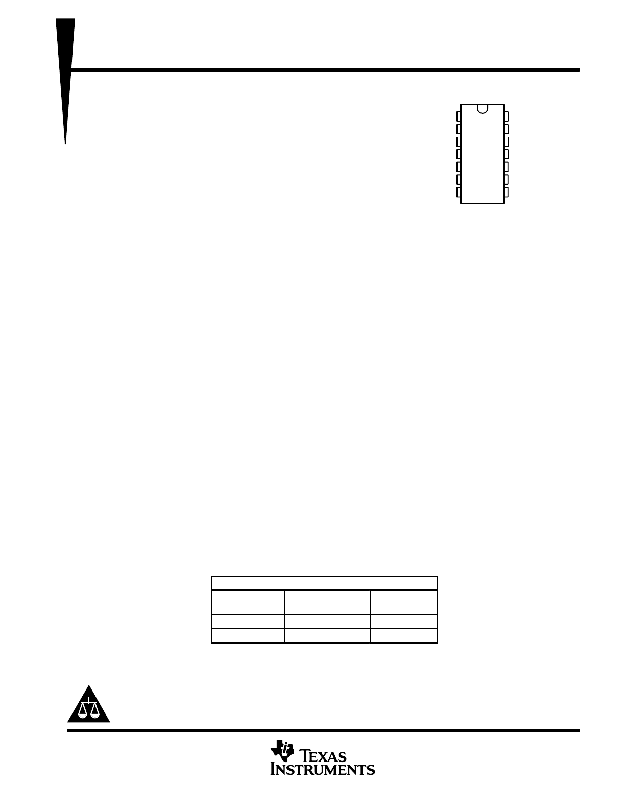
The 14-terminal small-outline (D) package allows digital control of analog functions in space-critical
applications. The TLC5620C is characterized for operation from 0
°
C to 70
°
C. The TLC5620I is characterized
for operation from – 40
°
C to 85
°
C. The TLC5620C and TLC5620I do not require external trimming.
AVAILABLE OPTIONS
PACKAGE
TA
SMALL OUTLINE
(D)
PLASTIC DIP
(N)
0
°
C to 70
°
C
TLC5620CD
TLC5620CN
– 40
°
C to 85
°
C
TLC5620ID
TLC5620IN
Please be aware that an important notice concerning availability, standard warranty, and use in critical applications of
Texas Instruments semiconductor products and disclaimers thereto appears at the end of this data sheet.
1
2
3
4
5
6
7
14
13
12
11
10
9
8
GND
REFA
REFB
REFC
REFD
DATA
CLK
V
DD
LDAC
DACA
DACB
DACC
DACD
LOAD
N OR D PACKAGE
(TOP VIEW)
PRODUCTION DATA information is current as of publication date.
Products conform to specifications per the terms of Texas Instruments
standard warranty. Production processing does not necessarily include
testing of all parameters.
Copyright
2001, Texas Instruments Incorporated
TLC5620C, TLC5620I
QUADRUPLE 8-BIT DIGITAL-TO-ANALOG CONVERTERS
SLAS081E – NOVEMBER 1994 – REVISED NOVEMBER 2001
2
POST OFFICE BOX 655303
•
DALLAS, TEXAS 75265
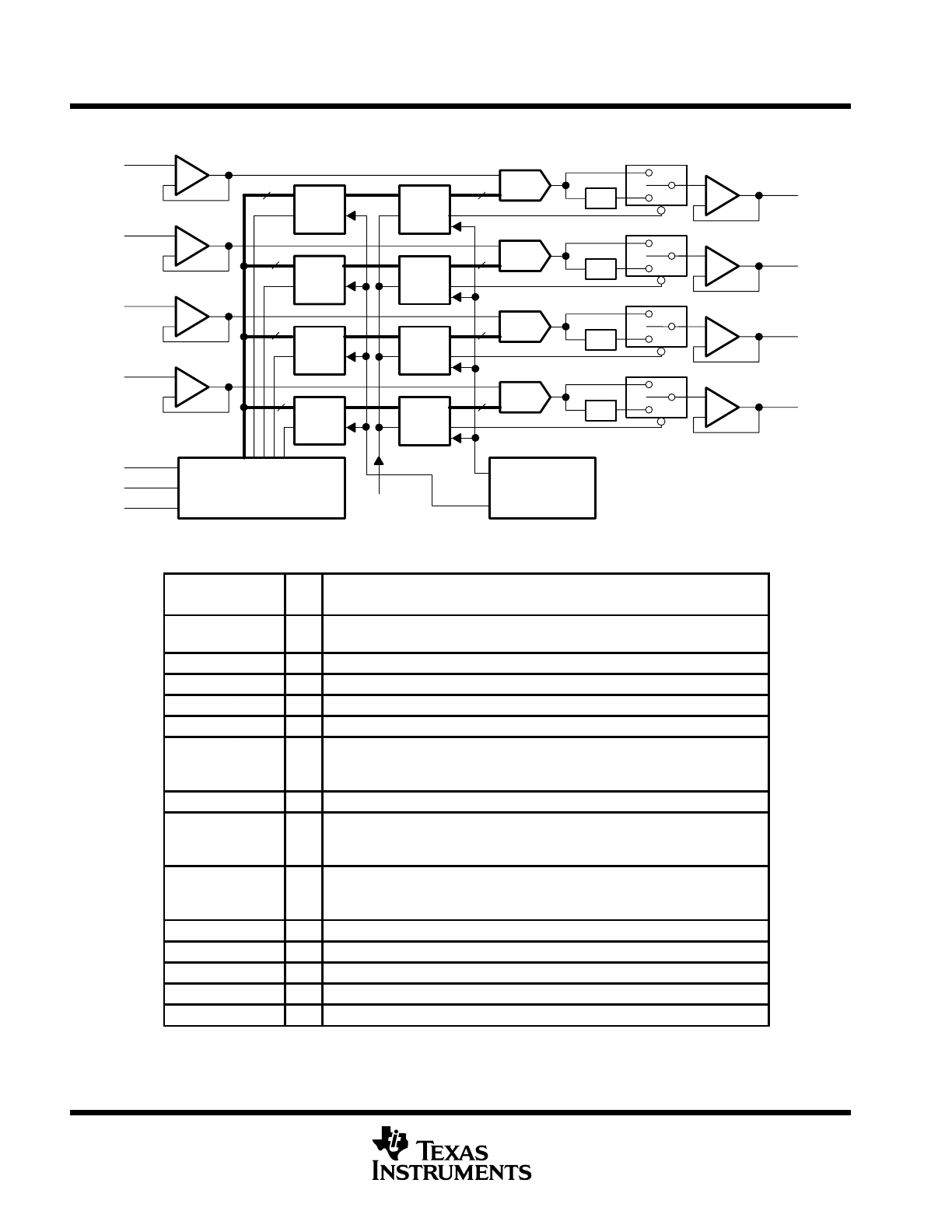
functional block diagram
DAC
DAC
Power-On
Reset
Serial
Interface
×
2
Latch
Latch
Latch
Latch
DAC
×
2
×
2
Latch
Latch
Latch
Latch
DAC
×
2
LDAC
REFA
+
–
+
–
+
–
+
–
+
–
+
–
+
–
+
–
REFB
REFC
CLK
REFD
DATA
LOAD
DACA
DACB
DACC
DACD
8
8
8
8
8
8
8
8
2
3
4
5
7
6
8
13
12
11
10
9
Terminal Functions
TERMINAL
I/O
DESCRIPTION
NAME
NO.
I/O
DESCRIPTION
CLK
7
I
Serial interface clock. The input digital data is shifted into the serial interface
register on the falling edge of the clock applied to the CLK terminal.
DACA
12
O
DAC A analog output
DACB
11
O
DAC B analog output
DACC
10
O
DAC C analog output
DACD
9
O
DAC D analog output
DATA
6
I
Serial interface digital data input. The digital code for the DAC is clocked into the
serial interface register serially. Each data bit is clocked into the register on the
falling edge of the clock signal.
GND
1
I
Ground return and reference terminal
LDAC
13
I
Load DAC. When the LDAC signal is high, no DAC output updates occur when
the input digital data is read into the serial interface. The DAC outputs are only
updated when LDAC is taken from high to low.
LOAD
8
I
Serial Interface load control. When LDAC is low, the falling edge of the LOAD
signal latches the digital data into the output latch and immediately produces the
analog voltage at the DAC output terminal.
REFA
2
I
Reference voltage input to DAC A. This voltage defines the output analog range.
REFB
3
I
Reference voltage input to DAC B. This voltage defines the output analog range.
REFC
4
I
Reference voltage input to DAC C. This voltage defines the output analog range.
REFD
5
I
Reference voltage input to DAC D. This voltage defines the output analog range.
VDD
14
I
Positive supply voltage
TLC5620C, TLC5620I
QUADRUPLE 8-BIT DIGITAL-TO-ANALOG CONVERTERS
SLAS081E – NOVEMBER 1994 – REVISED NOVEMBER 2001
3
POST OFFICE BOX 655303
•
DALLAS, TEXAS 75265
detailed description
The TLC5620 is implemented using four resistor-string DACs. The core of each DAC is a single resistor with
256 taps, corresponding to the 256 possible codes listed in Table 1. One end of each resistor string is connected
to the GND terminal and the other end is fed from the output of the reference input buffer. Monotonicity is
maintained by use of the resistor strings. Linearity depends upon the matching of the resistor elements and upon
the performance of the output buffer. Since the inputs are buffered, the DACs always present a high-impedance
load to the reference source.
Each DAC output is buffered by a configurable-gain output amplifier that can be programmed to times 1 or times
2 gain.
On power up, the DACs are reset to CODE 0.
Each output voltage is given by:
V
O
(DACA|B|C|D)
+
REF
CODE
256
(1
)
RNG bit value)
where CODE is in the range 0 to 255 and the range (RNG) bit is 0 or 1 within the serial control word.
Table 1. Ideal Output Transfer
D7
D6
D5
D4
D3
D2
D1
D0
OUTPUT VOLTAGE
0
0
0
0
0
0
0
0
GND
0
0
0
0
0
0
0
1
(1/256)
×
REF (1+RNG)
•
•
•
•
•
•
•
•
•
•
•
•
•
•
•
•
•
•
0
1
1
1
1
1
1
1
(127/256)
×
REF (1+RNG)
1
0
0
0
0
0
0
0
(128/256)
×
REF (1+RNG)
•
•
•
•
•
•
•
•
•
•
•
•
•
•
•
•
•
•
1
1
1
1
1
1
1
1
(255/256)
×
REF (1+RNG)
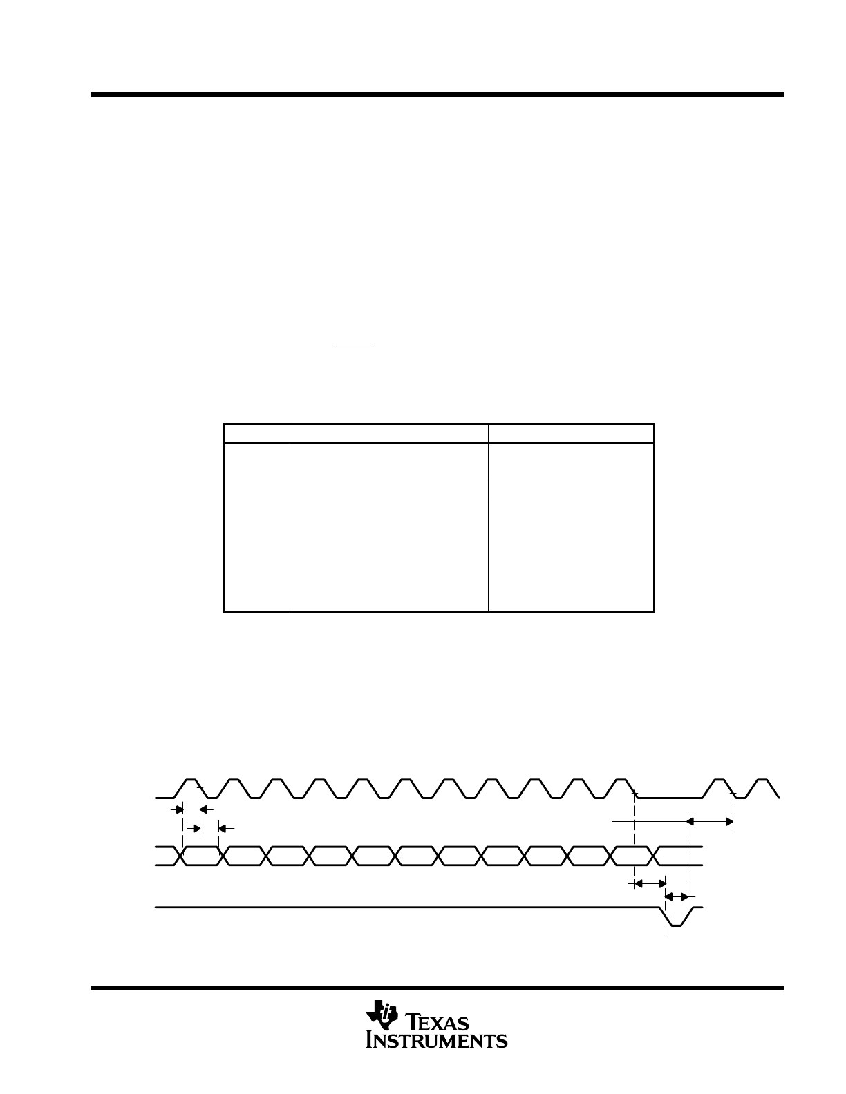
data interface
With LOAD high, data is clocked into the DATA terminal on each falling edge of CLK. Once all data bits have
been clocked in, LOAD is pulsed low to transfer the data from the serial input register to the selected DAC as
shown in Figure 1. When LDAC is low, the selected DAC output voltage is updated when LOAD goes low. When
LDAC is high during serial programming, the new value is stored within the device and can be transferred to
the DAC output at a later time by pulsing LDAC low as shown in Figure 2. Data is entered most significant bit
(MSB) first. Data transfers using two 8-clock cycle periods are shown in Figures 3 and 4.
RNG
A1
A0
D7
D6
D5
D4
D3
D2
D1
D0
DAC Update
CLK
DATA
LOAD
tsu(DATA-CLK)
tv(DATA-CLK)
tsu(CLK-LOAD)
tw(LOAD)
tsu(LOAD-CLK)
Figure 1. LOAD-Controlled Update (LDAC = Low)
TLC5620C, TLC5620I
QUADRUPLE 8-BIT DIGITAL-TO-ANALOG CONVERTERS
SLAS081E – NOVEMBER 1994 – REVISED NOVEMBER 2001
4
POST OFFICE BOX 655303
•
DALLAS, TEXAS 75265
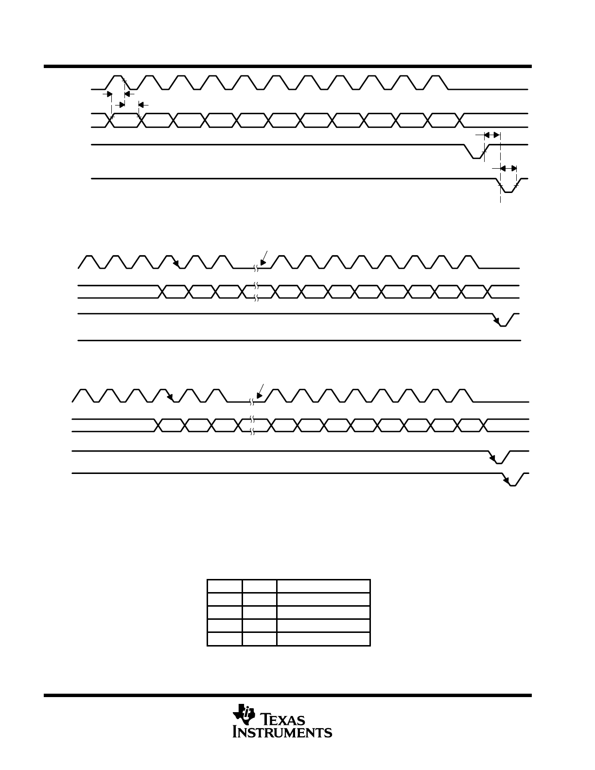
RNG
CLK
DATA
LOAD
LDAC
DAC Update
A1
A0
D7
D6
D5
D4
D3
D2
D1
D0
tsu(DATA-CLK)
tv(DATA-CLK)
tw(LDAC)
tsu(LOAD-LDAC)
Figure 2. LDAC-Controlled Update
ÎÎÎÎÎÎ
ÎÎÎ
ÎÎÎ
A1
A0
RNG
D7
D6
D5
D4
D3
D2
D1
D0
CLK
DATA
LOAD
LDAC
CLK Low
Figure 3. Load-Controlled Update Using 8-Bit Serial Word (LDAC = Low)
ÎÎÎÎÎÎÎ
ÎÎÎÎ
ÎÎÎÎ
A1
A0
RNG
D7
D6
D5
D4
D3
D2
D1
D0
CLK
DATA
LOAD
LDAC
CLK Low
Figure 4. LDAC-Controlled Update Using 8-Bit Serial Word
Table 2 lists the A1 and A0 bits and the selection of the updated DACs. The RNG bit controls the DAC output
range. When RNG = low, the output range is between the applied reference voltage and GND, and when
RNG = high, the range is between twice the applied reference voltage and GND.
Table 2. Serial Input Decode
A1
A0
DAC UPDATED
0
0
DACA
0
1
DACB
1
0
DACC
1
1
DACD
TLC5620C, TLC5620I
QUADRUPLE 8-BIT DIGITAL-TO-ANALOG CONVERTERS
SLAS081E – NOVEMBER 1994 – REVISED NOVEMBER 2001
5
POST OFFICE BOX 655303
•
DALLAS, TEXAS 75265
linearity, offset, and gain error using single-end supplies
When an amplifier is operated from a single supply, the voltage offset can still be either positive or negative. With
a positive offset voltage, the output voltage changes on the first code change. With a negative offset the output
voltage may not change with the first code depending on the magnitude of the offset voltage.
The output amplifier attempts to drive the output to a negative voltage. However, because the most negative
supply rail is ground, the output cannot drive below ground and clamps the output at 0 V.
The output voltage then remains at zero until the input code value produces a sufficient positive output voltage
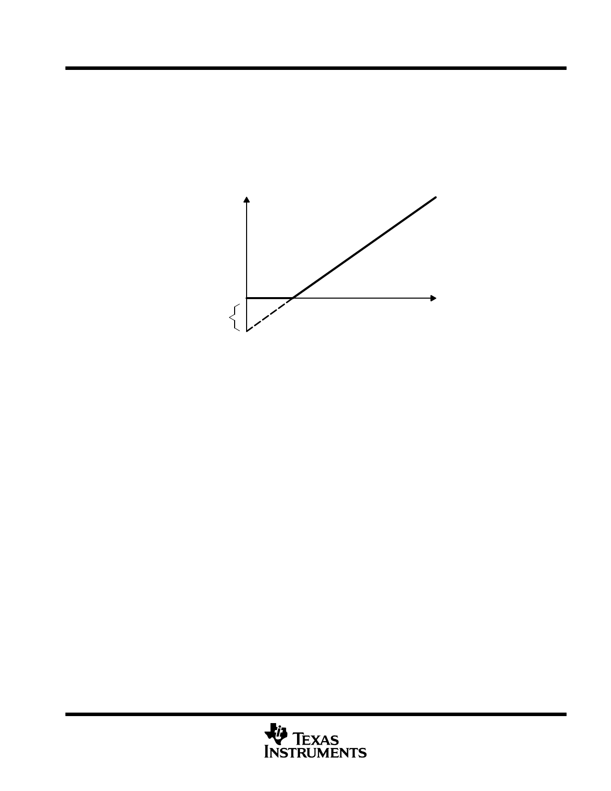
to overcome the negative offset voltage, resulting in the transfer function shown in Figure 5.
DAC Code
Output
Voltage
0 V
Negative
Offset
Figure 5. Effect of Negative Offset (Single Supply)
This offset error, not the linearity error, produces this breakpoint. The transfer function would have followed the
dotted line if the output buffer could drive below ground.
For a DAC, linearity is measured between zero-input code (all inputs 0) and full-scale code (all inputs 1) after
offset and full scale are adjusted out or accounted for in some way. However, single-supply operation does not
allow for adjustment when the offset is negative due to the breakpoint in the transfer function. So the linearity
is measured between full-scale code and the lowest code that produces a positive output voltage. The code is
calculated from the maximum specification for the negative offset voltage.
TLC5620C, TLC5620I
QUADRUPLE 8-BIT DIGITAL-TO-ANALOG CONVERTERS
SLAS081E – NOVEMBER 1994 – REVISED NOVEMBER 2001
6
POST OFFICE BOX 655303
•
DALLAS, TEXAS 75265
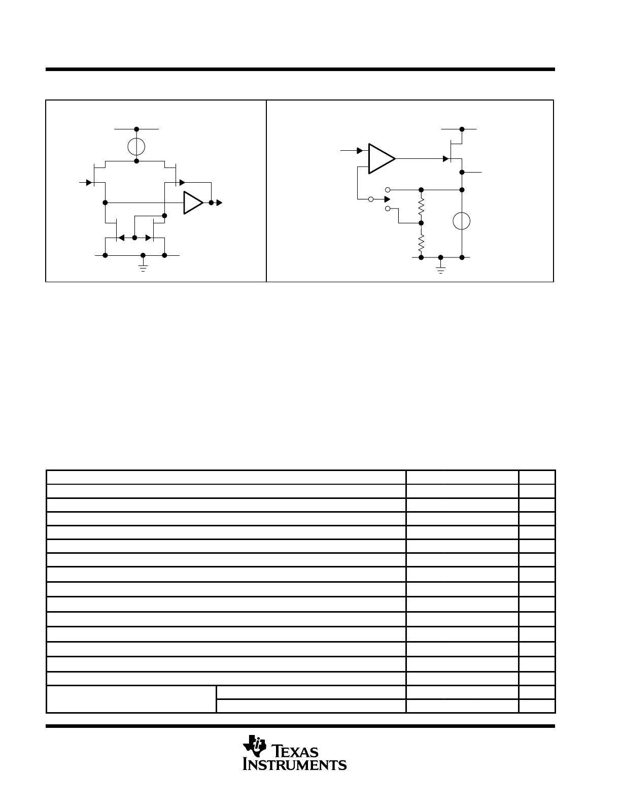
equivalent inputs and outputs
GND
Vref
Input
VDD
To DAC
Resistor
String
_
+
VDD
DAC
Voltage Output
ISINK
60
µ
A
Typical
84 k
Ω
84 k
Ω
×
1
×
2
Output
Range
Select
Input from
Decoded DAC
Register String
INPUT CIRCUIT
OUTPUT CIRCUIT
GND
absolute maximum ratings over operating free-air temperature range (unless otherwise noted)
†
Supply voltage (V
DD
– GND)
7 V
. . . . . . . . . . . . . . . . . . . . . . . . . . . . . . . . . . . . . . . . . . . . . . . . . . . . . . . . . . . . . . . . .
Digital input voltage range
GND – 0.3 V to V
DD
+ 0.3 V
. . . . . . . . . . . . . . . . . . . . . . . . . . . . . . . . . . . . . . . . . . . . .
Reference input voltage range, V
ID
GND
– 0.3 V to V
DD
+ 0.3 V
. . . . . . . . . . . . . . . . . . . . . . . . . . . . . . . . . . . . . .
Operating free-air temperature range, T
A
: TLC5620C 0
°
C to 70
°
C
. . . . . . . . . . . . . . . . . . . . . . . . . . . . . . . . . . . .
TLC5620I
– 40
°
C to 85
°
C
. . . . . . . . . . . . . . . . . . . . . . . . . . . . . . . . . . .
Storage temperature range, T
stg
– 50
°
C to 150
°
C
. . . . . . . . . . . . . . . . . . . . . . . . . . . . . . . . . . . . . . . . . . . . . . . . . . .
Lead temperature 1,6 mm (1/16 inch) from case for 10 seconds
260
°
C
. . . . . . . . . . . . . . . . . . . . . . . . . . . . . . .
† Stresses beyond those listed under “absolute maximum ratings” may cause permanent damage to the device. These are stress ratings only, and
functional operation of the device at these or any other conditions beyond those indicated under “recommended operating conditions” is not
implied. Exposure to absolute-maximum-rated conditions for extended periods may affect device reliability.
recommended operating conditions
MIN
NOM
MAX
UNIT
Supply voltage, VDD
4.75
5.25
V
High-level input voltage, VIH
0.8 VDD
V
Low-level input voltage, VIL
0.8
V
Reference voltage, Vref [A|B|C|D]
VDD – 1.5
V
Analog full-scale output voltage, RL = 10 k
Ω
3.5
V
Load resistance, RL
10
k
Ω
Setup time, data input, tsu(DATA-CLK) (see Figures 1 and 2)
50
ns
Valid time, data input valid after CLK
↓
, tv(DATA-CLK) (see Figures 1 and 2)
50
ns
Setup time, CLK eleventh falling edge to LOAD, tsu(CLK-LOAD) (see Figure 1)
50
ns
Setup time, LOAD
↑
to CLK
↓
, tsu(LOAD-CLK) (see Figure 1)
50
ns
Pulse duration, LOAD, tw(LOAD) (see Figure 1)
250
ns
Pulse duration, LDAC, tw(LDAC) (see Figure 2)
250
ns
Setup time, LOAD
↑
to LDAC
↓
, tsu(LOAD-LDAC) (see Figure 2)
0
ns
CLK frequency
1
MHz
Operating free air temperature TA
TLC5620C
0
70
°
C
Operating free-air temperature, TA
TLC5620I
– 40
85
°
C
TLC5620C, TLC5620I
QUADRUPLE 8-BIT DIGITAL-TO-ANALOG CONVERTERS
SLAS081E – NOVEMBER 1994 – REVISED NOVEMBER 2001
7
POST OFFICE BOX 655303
•
DALLAS, TEXAS 75265
electrical characteristics over recommended operating free-air temperature range, V
DD
= 5 V
±
5%,
V
ref
= 2 V,
×
1 gain output range (unless otherwise noted)
PARAMETER
TEST CONDITIONS
MIN
TYP
MAX
UNIT
IIH
High-level input current
VI = VDD
±
10
µ
A
IIL
Low-level input current
VI = 0 V
±
10
µ
A
IO(sink)
Output sink current
Each DAC output
20
µ
A
IO(source)
Output source current
Each DAC output
2
mA
Ci
Input capacitance
15
pF
Ci
Reference input capacitance
15
pF
IDD
Supply current
VDD = 5 V
2
mA
Iref
Reference input current
VDD = 5 V,
Vref = 2 V
±
10
µ
A
EL
Linearity error (end point corrected)
Vref = 2 V,
×
2 gain (see Note 1)
±
1
LSB
ED
Differential-linearity error
Vref = 2 V,
×
2 gain (see Note 2)
±
0.9
LSB
EZS
Zero-scale error
Vref = 2 V,
×
2 gain (see Note 3)
0
30
mV
Zero-scale-error temperature coefficient
Vref = 2 V,
×
2 gain (see Note 4)
10
µ
V/
°
C
EFS
Full-scale error
Vref = 2 V,
×
2 gain (see Note 5)
±
60
mV
Full-scale-error temperature coefficient
Vref = 2 V,
×
2 gain (see Note 6)
±
25
µ
V/
°
C
PSRR
Power-supply rejection ratio
See Notes 7 and 8
0.5
mV/V
NOTES:
1. Integral nonlinearity (INL) is the maximum deviation of the output from the line between zero and full scale (excluding the effects
of zero code and full-scale errors).
2. Differential nonlinearity (DNL) is the difference between the measured and ideal 1 LSB amplitude change of any two adjacent codes.
Monotonic means the output voltage changes in the same direction (or remains constant) as a change in the digital input code.
3. Zero-scale error is the deviation from zero voltage output when the digital input code is zero.
4. Zero-scale-error temperature coefficient is given by: ZSETC = [ZSE(Tmax) – ZSE(Tmin)]/Vref
×
106/(Tmax – Tmin).
5. Full-scale error is the deviation from the ideal full-scale output (Vref – 1 LSB) with an output load of 10 k
Ω
.
6. Full-scale-error temperature coefficient is given by: FSETC = [FSE(Tmax) – FSE (Tmin)]/Vref
×
106/(Tmax – Tmin).
7. Zero-scale-error rejection ratio (ZSE RR) is measured by varying the VDD from 4.5 V to 5.5 V dc and measuring the proportion of
this signal imposed on the zero-code output voltage.
8. Full-scale-error rejection ratio (FSE RR) is measured by varying the VDD from 4.5 V to 5.5 V dc and measuring the proportion of
this signal imposed on the full-scale output voltage.
operating characteristics over recommended operating free-air temperature range, V
DD
= 5 V
±
5%,
V
ref
= 2 V,
×
1 gain output range (unless otherwise noted)
TEST CONDITIONS
MIN
TYP
MAX
UNIT
Output slew rate
CL = 100 pF,
RL = 10 k
Ω
1
V/
µ
s
Output settling time
To
±
0.5 LSB,
CL = 100 pF,
RL = 10 k
Ω
,
See Note 9
10
µ
s
Large-signal bandwidth
Measured at – 3 dB point
100
kHz
Digital crosstalk
CLK = 1-MHz square wave measured at DACA-DACD
– 50
dB
Reference feedthrough
See Note 10
– 60
dB
Channel-to-channel isolation
See Note 11
– 60
dB
Reference input bandwidth
See Note 12
100
kHz
NOTES:
9. Settling time is the time between a LOAD falling edge and the DAC output reaching full scale voltage within +/– 0.5 LSB starting from
an initial output voltage equal to zero.
10. Reference feedthrough is measured at any DAC output with an input code = 00 hex with a Vref input = 1 V dc + 1 Vpp at 10 kHz.
11. Channel-to-channel isolation is measured by setting the input code of one DAC to FF hex and the code of all other DACs to 00 hex
with Vref input = 1 V dc + 1 Vpp at 10 kHz.
12. Reference bandwidth is the –3 dB bandwidth with an input at Vref = 1.25 V dc + 2 Vpp and with a full-scale digital-input code.
TLC5620C, TLC5620I
QUADRUPLE 8-BIT DIGITAL-TO-ANALOG CONVERTERS
SLAS081E – NOVEMBER 1994 – REVISED NOVEMBER 2001
8
POST OFFICE BOX 655303
•
DALLAS, TEXAS 75265
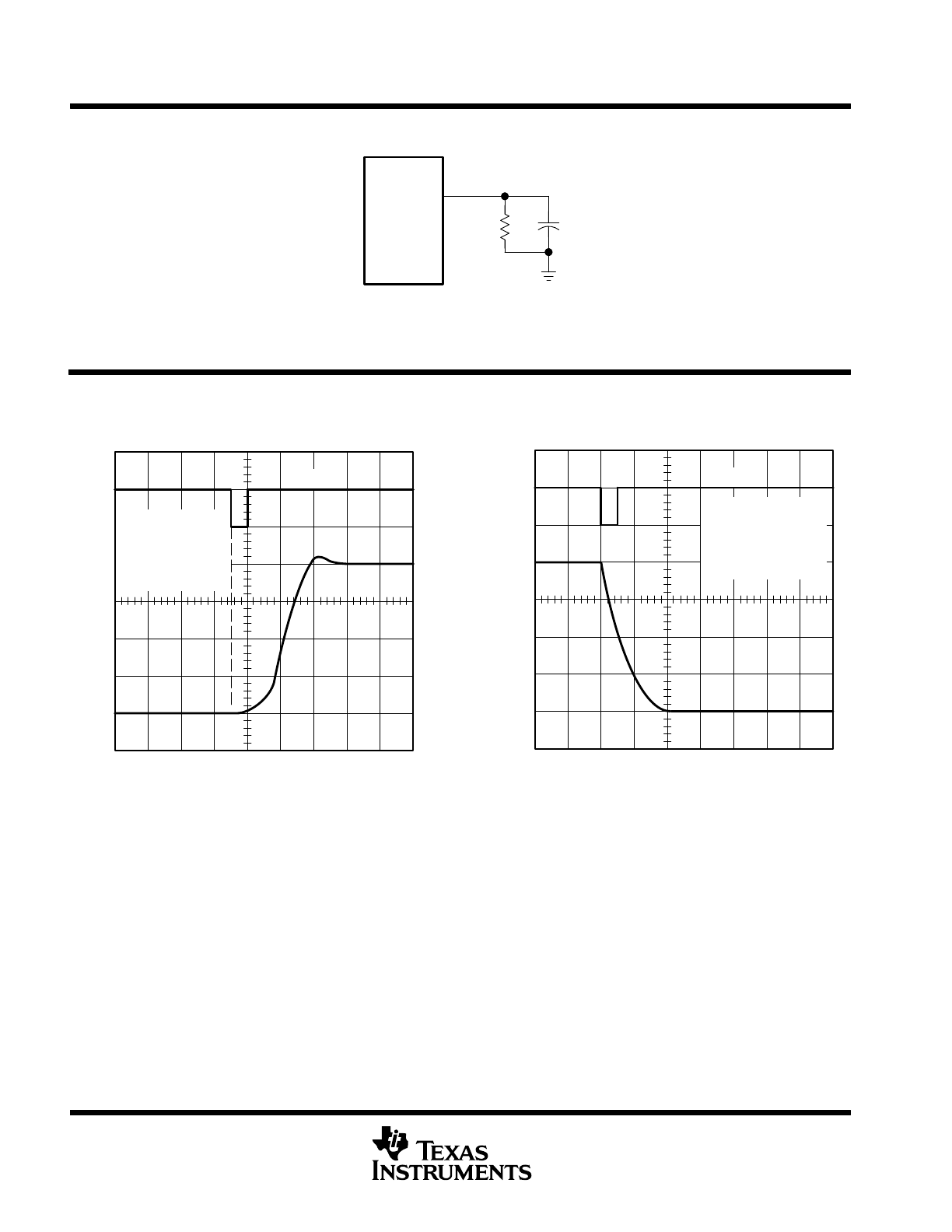
PARAMETER MEASUREMENT INFORMATION
10 k
Ω
CL = 100 pF
TLC5620
DACA
DACB
•
•
•
DACD
Figure 6. Slew, Settling Time, and Linearity Measurements
TYPICAL CHARACTERISTICS
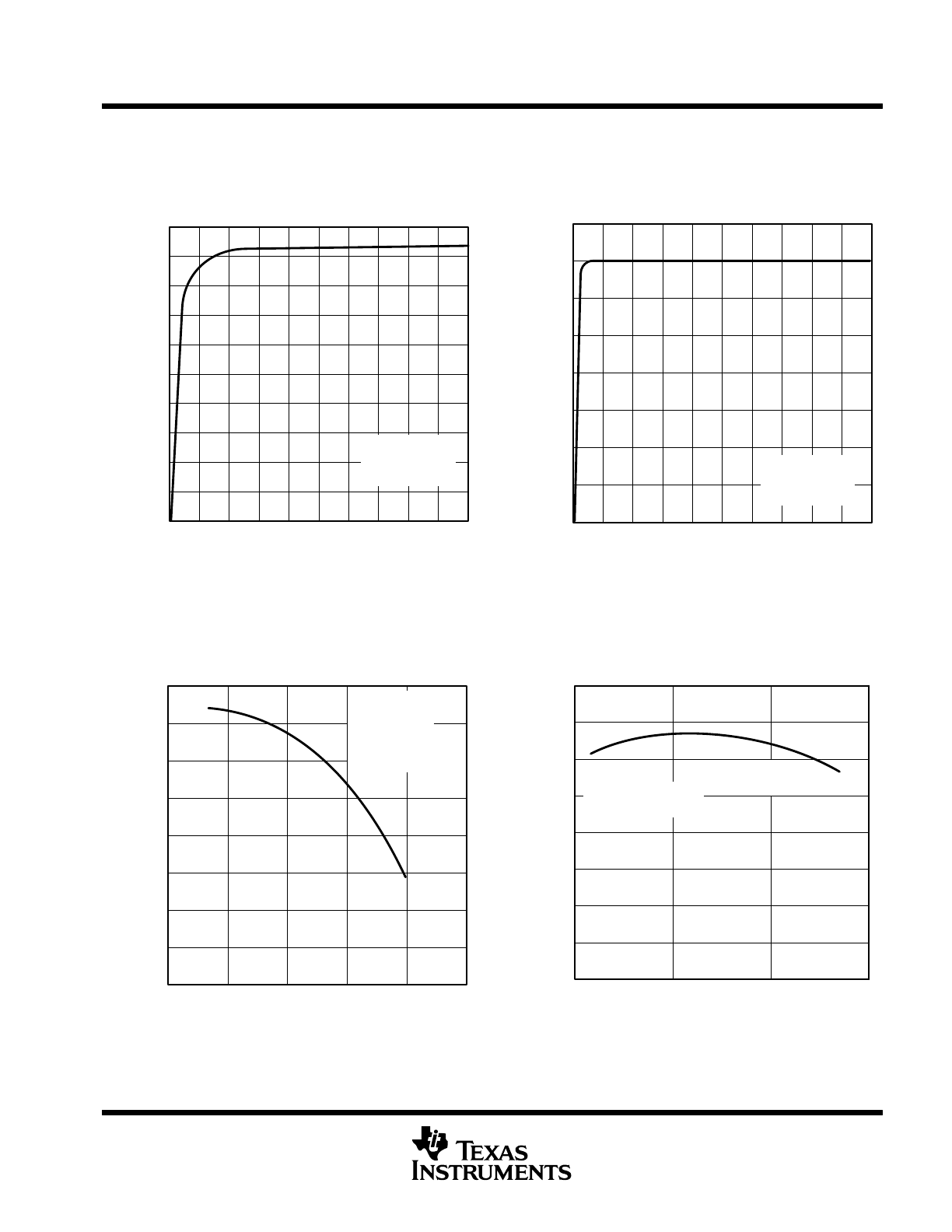
Figure 7
0
2
4
6
8
10
12
14
16
18
t – Time –
µ
s
VDD = 5 V
TA = 25
°
C
Code 00 to FF Hex
Range =
×
2
Vref = 2 V
3
1
0
2
LDAC
–
Output V
oltage
–
V
V
O
POSITIVE RISE AND SETTLING TIME
Figure 8
0
2
4
6
8
10
12
14
16
18
t – Time –
µ
s
3
1
0
2
LDAC
VDD = 5 V
TA = 25
°
C
Code FF to 00 Hex
Range =
×
2
Vref = 2 V
–
Output V
oltage
–
V
V
O
NEGATIVE FALL AND SETTLING TIME
TLC5620C, TLC5620I
QUADRUPLE 8-BIT DIGITAL-TO-ANALOG CONVERTERS
SLAS081E – NOVEMBER 1994 – REVISED NOVEMBER 2001
9
POST OFFICE BOX 655303
•
DALLAS, TEXAS 75265
TYPICAL CHARACTERISTICS
Figure 9
4
3.8
3.4
3.2
3
4.8
3.6
0
10
20
30
40
50
60
–
DAC Output V
oltage
–
V
4.4
4.2
4.6
DAC OUTPUT VOLTAGE
vs
OUTPUT LOAD
5
70
80
90
100
V
O
RL – Output Load – k
Ω
VDD = 5 V,
Vref = 2.5 V,
Range = 2x
Figure 10
2
1.5
0.5
0
0
10
20
30
40
50
60
2.5
3.5
4
70
80
90
100
1
3
DAC OUTPUT VOLTAGE
vs
OUTPUT LOAD
VDD = 5 V,
Vref = 3.5 V,
Range = 1x
–
DAC Output V
oltage
–
V
V
O
RL – Output Load – k
Ω
Figure 11
4
3
1
0
0
1
2
3
–
Output Source Current
–
mA
5
7
OUTPUT SOURCE CURRENT
vs
OUTPUT VOLTAGE
8
4
5
2
6
VDD = 5 V
TA = 25
°
C
Vref = 2 V
Range =
×
2
Input Code = 255
I O(source)
VO – Output Voltage – V
Figure 12
1
0.9
0.85
0.8
–
Supply Current
–
mA
1.1
1.15
SUPPLY CURRENT
vs
TEMPERATURE
1.2
1.05
0.95
– 50
0
50
100
VDD = 5 V
Vref 2 V
Range =
×
2
Input Code = 255
I DD
t – Temperature –
°
C
TLC5620C, TLC5620I
QUADRUPLE 8-BIT DIGITAL-TO-ANALOG CONVERTERS
SLAS081E – NOVEMBER 1994 – REVISED NOVEMBER 2001
10
POST OFFICE BOX 655303
•
DALLAS, TEXAS 75265
TYPICAL CHARACTERISTICS
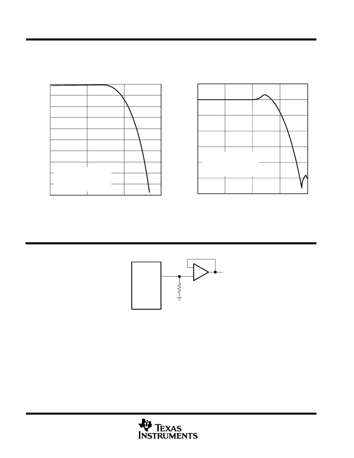
Figure 13
1
10
100
G
–
Relative Gain
–
dB
f – Frequency – kHz
RELATIVE GAIN
vs
FREQUENCY
1000
0
– 2
– 4
– 6
– 8
– 10
– 12
– 14
– 16
– 18
– 20
VDD = 5 V
TA = 25
°
C
Vref = 1.25 Vdc + 2 Vpp
Input Code = 255
Figure 14
1
10
100
1000
G
–
Relative Gain
–
dB
f – Frequency – kHz
RELATIVE GAIN
vs
FREQUENCY
10000
10
0
– 10
– 20
– 30
– 40
– 50
– 60
VDD = 5 V
TA = 25
°
C
Vref = 2 Vdc + 0.5 Vpp
Input Code = 255
APPLICATION INFORMATION
NOTE A: Resistor R
w
10 k
Ω
R
TLC5620
DACA
DACB
•
•
•
DACD
_
+
VO
Figure 15. Output Buffering Scheme
TLC5620C, TLC5620I
QUADRUPLE 8-BIT DIGITAL-TO-ANALOG CONVERTERS
SLAS081E – NOVEMBER 1994 – REVISED NOVEMBER 2001
11
POST OFFICE BOX 655303
•
DALLAS, TEXAS 75265
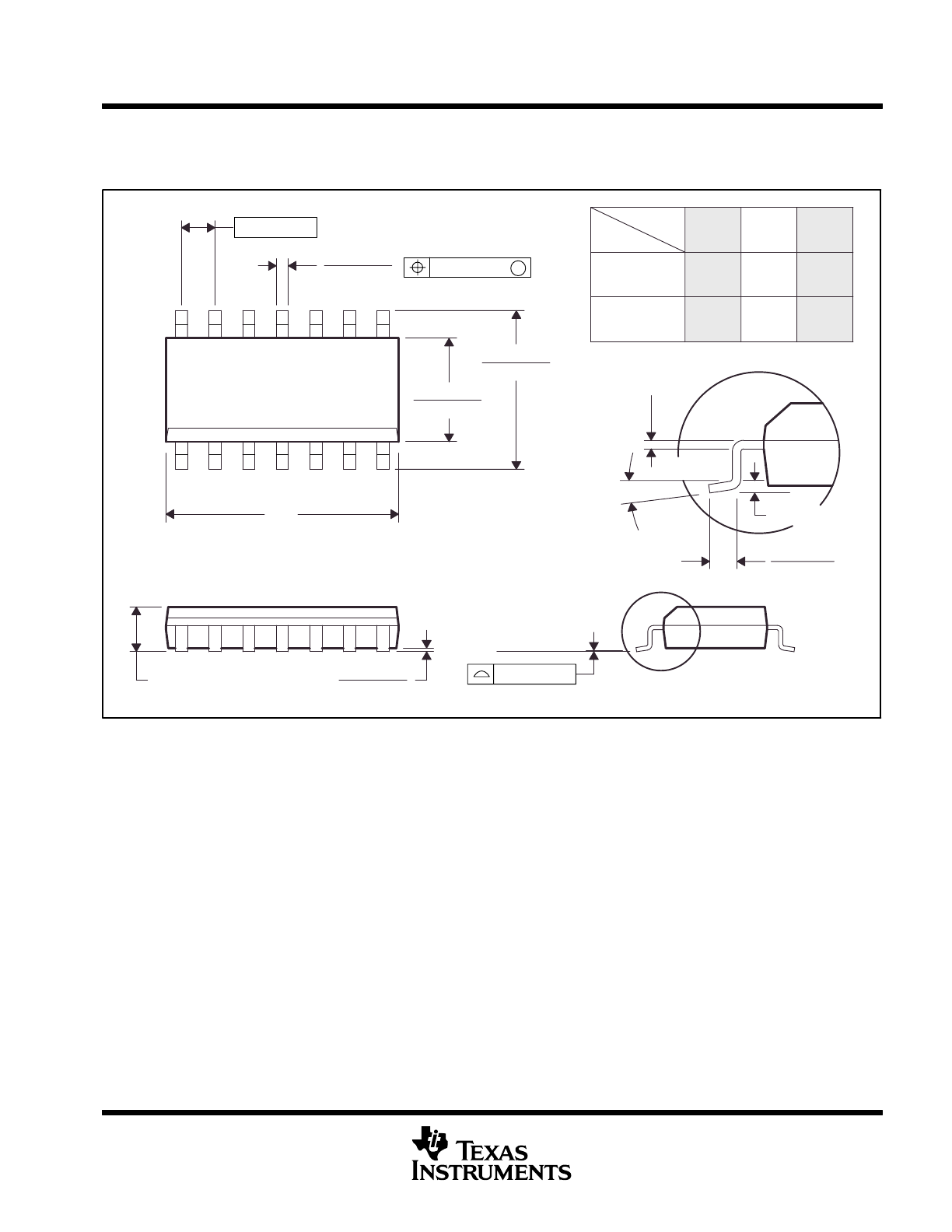
MECHANICAL DATA
D (R-PDSO-G**)
PLASTIC SMALL-OUTLINE PACKAGE
14 PIN SHOWN
4040047 / B 10/94
0.228 (5,80)
0.244 (6,20)
0.069 (1,75) MAX
0.010 (0,25)
0.004 (0,10)
1
14
0.014 (0,35)
0.020 (0,51)
A
0.157 (4,00)
0.150 (3,81)
7
8
0.044 (1,12)
0.016 (0,40)
Seating Plane
0.010 (0,25)
PINS **
0.008 (0,20) NOM
A MIN
A MAX
DIM
Gage Plane
0.189
(4,80)
(5,00)
0.197
8
(8,55)
(8,75)
0.337
14
0.344
(9,80)
16
0.394
(10,00)
0.386
0.004 (0,10)
M
0.010 (0,25)
0.050 (1,27)
0
°
– 8
°
NOTES: A. All linear dimensions are in inches (millimeters).
B. This drawing is subject to change without notice.
C. Body dimensions do not include mold flash or protrusion not to exceed 0.006 (0,15).
D. Four center pins are connected to die mount pad.
E. Falls within JEDEC MS-012
TLC5620C, TLC5620I
QUADRUPLE 8-BIT DIGITAL-TO-ANALOG CONVERTERS
SLAS081E – NOVEMBER 1994 – REVISED NOVEMBER 2001
12
POST OFFICE BOX 655303
•
DALLAS, TEXAS 75265
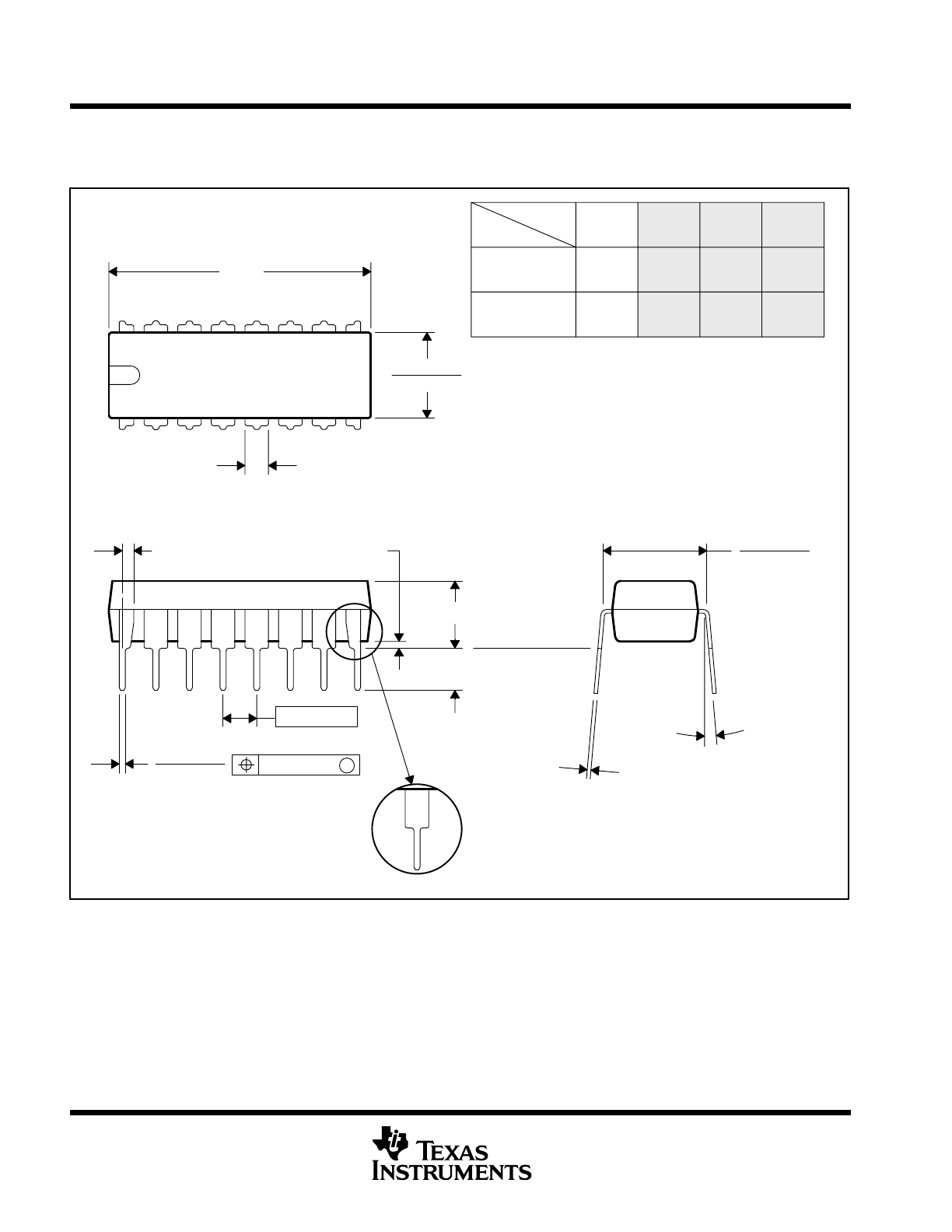
MECHANICAL DATA
N (R-PDIP-T**)
PLASTIC DUAL-IN-LINE PACKAGE
20
0.975
(24,77)
0.940
(23,88)
18
0.920
0.850
14
0.775
0.745
(19,69)
(18,92)
16
0.775
(19,69)
(18,92)
0.745
A MIN
DIM
A MAX
PINS **
0.310 (7,87)
0.290 (7,37)
(23.37)
(21.59)
Seating Plane
0.010 (0,25) NOM
14/18 PIN ONLY
4040049/C 08/95
9
8
0.070 (1,78) MAX
A
0.035 (0,89) MAX
0.020 (0,51) MIN
16
1
0.015 (0,38)
0.021 (0,53)
0.200 (5,08) MAX
0.125 (3,18) MIN
0.240 (6,10)
0.260 (6,60)
M
0.010 (0,25)
0.100 (2,54)
0
°
– 15
°
16 PIN SHOWN
NOTES: A. All linear dimensions are in inches (millimeters).
B. This drawing is subject to change without notice.
C. Falls within JEDEC MS-001 (20-pin package is shorter than MS-001)

IMPORTANT NOTICE
Texas Instruments Incorporated and its subsidiaries (TI) reserve the right to make corrections, modifications,
enhancements, improvements, and other changes to its products and services at any time and to discontinue
any product or service without notice. Customers should obtain the latest relevant information before placing
orders and should verify that such information is current and complete. All products are sold subject to TI’s terms
and conditions of sale supplied at the time of order acknowledgment.
TI warrants performance of its hardware products to the specifications applicable at the time of sale in
accordance with TI’s standard warranty. Testing and other quality control techniques are used to the extent TI
deems necessary to support this warranty. Except where mandated by government requirements, testing of all
parameters of each product is not necessarily performed.
TI assumes no liability for applications assistance or customer product design. Customers are responsible for
their products and applications using TI components. To minimize the risks associated with customer products
and applications, customers should provide adequate design and operating safeguards.
TI does not warrant or represent that any license, either express or implied, is granted under any TI patent right,
copyright, mask work right, or other TI intellectual property right relating to any combination, machine, or process
in which TI products or services are used. Information published by TI regarding third–party products or services
does not constitute a license from TI to use such products or services or a warranty or endorsement thereof.
Use of such information may require a license from a third party under the patents or other intellectual property
of the third party, or a license from TI under the patents or other intellectual property of TI.
Reproduction of information in TI data books or data sheets is permissible only if reproduction is without
alteration and is accompanied by all associated warranties, conditions, limitations, and notices. Reproduction
of this information with alteration is an unfair and deceptive business practice. TI is not responsible or liable for
such altered documentation.
Resale of TI products or services with statements different from or beyond the parameters stated by TI for that
product or service voids all express and any implied warranties for the associated TI product or service and
is an unfair and deceptive business practice. TI is not responsible or liable for any such statements.
Mailing Address:
Texas Instruments
Post Office Box 655303
Dallas, Texas 75265
Copyright
2001, Texas Instruments Incorporated