
MC3486
QUADRUPLE DIFFERENTIAL LINE RECEIVER
WITH 3-STATE OUTPUTS
SLLS097B – JUNE 1980 – REVISED MAY 1995
1
POST OFFICE BOX 655303
•
DALLAS, TEXAS 75265
D
Meets or Exceeds the Requirements of
ANSI Standards EIA/TIA-422-B and
EIA/TIA-423-B and ITU Recommendations
V.10 and V.11
D
3-State, TTL-Compatible Outputs
D
Fast Transition Times
D
Operates From Single 5-V Supply
D
Designed to Be Interchangeable With
Motorola
MC3486
description
The MC3486 is a monolithic quadruple differential line receiver designed to meet the specifications of ANSI
Standards EIA/TIA-422-B and EIA/TIA-423-B and ITU Recommendations V.10 and V.11. The MC3486 offers
four independent differential-input line receivers that have TTL-compatible outputs. The outputs utilize 3-state
circuitry to provide a high-impedance state at any output when the appropriate output enable is at a low logic
level.
The MC3486 is designed for optimum performance when used with the MC3487 quadruple differential line
driver. It is supplied in a 16-pin package and operates from a single 5-V supply.
The MC3486 is characterized for operation from 0
°
C to 70
°
C.
FUNCTION TABLE
(each receiver)
DIFFERENTIAL INPUTS
ENABLE
OUTPUT
A–B
ENABLE
Y
VID
≤
0.2 V
H
H
– 0.2 V < VID < 0.2 V
H
?
VID
≤
– 0.2 V
H
L
Irrelevant
L
Z
Open
H
?
H = high level, L = low level, Z = high impedance (off),
? = indeterminate
Copyright
1995, Texas Instruments Incorporated
PRODUCTION DATA information is current as of publication date.
Products conform to specifications per the terms of Texas Instruments
standard warranty. Production processing does not necessarily include
testing of all parameters.
Motorola is a trademark of Motorola, Incorporated.
Please be aware that an important notice concerning availability, standard warranty, and use in critical applications of
Texas Instruments semiconductor products and disclaimers thereto appears at the end of this data sheet.
1
2
3
4
5
6
7
8
16
15
14
13
12
11
10
9
1B
1A
1Y
1,2EN
2Y
2A
2B
GND
V
CC
4B
4A
4Y
3,4EN
3Y
3A
3B
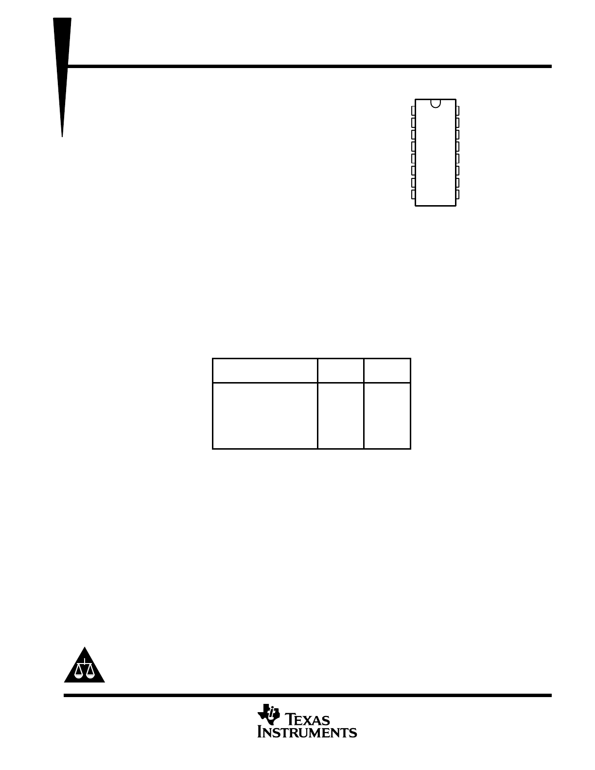
D OR N PACKAGE
(TOP VIEW)
MC3486
QUADRUPLE DIFFERENTIAL LINE RECEIVER
WITH 3-STATE OUTPUTS
SLLS097B – JUNE 1980 – REVISED MAY 1995
2
POST OFFICE BOX 655303
•
DALLAS, TEXAS 75265
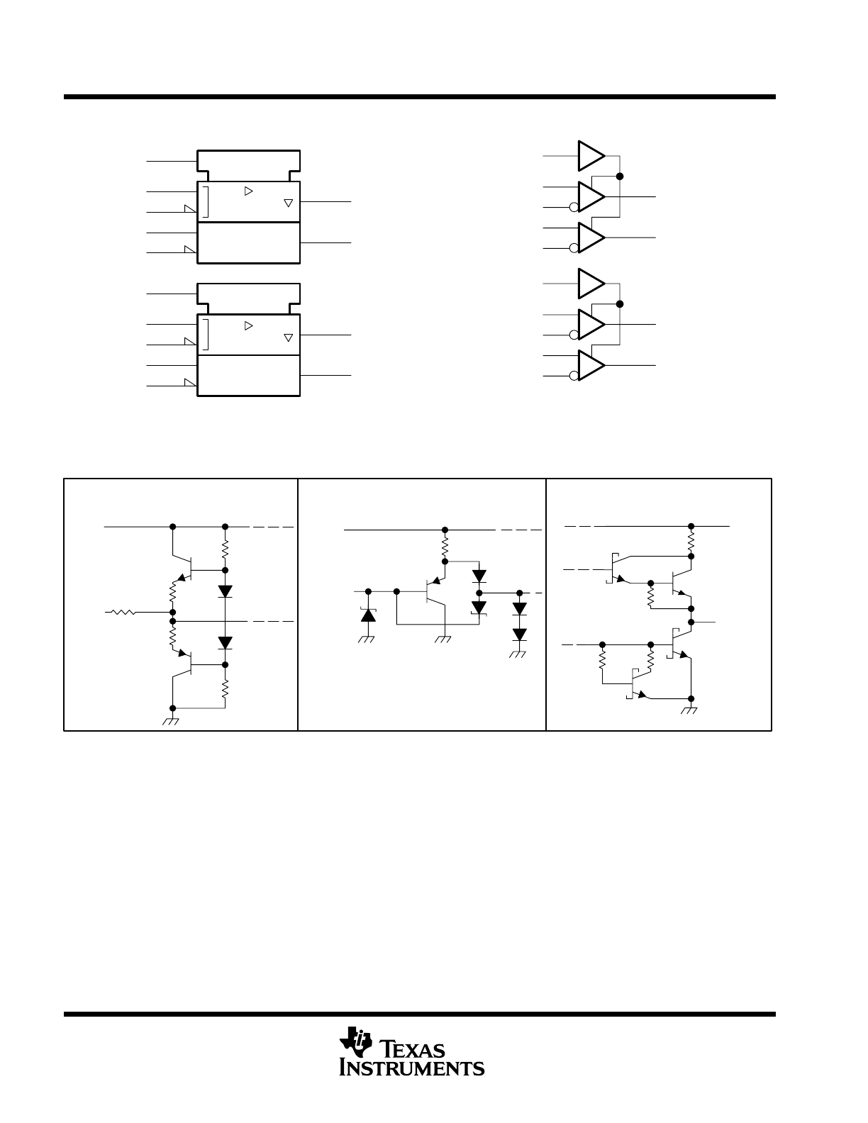
logic symbol
†
EN
EN
4B
4A
3B
3A
3, 4EN
13
11
4Y
3Y
15
14
9
10
12
2Y
1Y
2B
2A
1B
1A
1, 2EN
7
6
1
2
4
5
3
† This symbol is in accordance with ANSI/IEEE Std 91-1984
and IEC Publication 617-12.
logic diagram (positive logic)
4Y
3Y
2Y
1Y
15
14
9
10
12
7
6
1
2
4
4B
4A
3B
3A
3, 4EN
2B
2A
1B
1A
1, 2EN
13
11
5
3
schematics of inputs and outputs
16.8 k
Ω
NOM
Input
960
Ω
NOM
VCC
EQUIVALENT OF EACH INPUT
EXCEPT OUTPUT ENABLE
EQUIVALENT OF OUTPUT ENABLE
TYPICAL OF ALL OUTPUTS
VCC
Output
Enable
Output
VCC
4.9 k
Ω
NOM
85
Ω
NOM
8.3 k
Ω
NOM
960
Ω
NOM
MC3486
QUADRUPLE DIFFERENTIAL LINE RECEIVER
WITH 3-STATE OUTPUTS
SLLS097B – JUNE 1980 – REVISED MAY 1995
3
POST OFFICE BOX 655303
•
DALLAS, TEXAS 75265
absolute maximum ratings over operating free-air temperature range (unless otherwise noted)
†
Supply voltage, V
CC
(see Note 1)
8 V
. . . . . . . . . . . . . . . . . . . . . . . . . . . . . . . . . . . . . . . . . . . . . . . . . . . . . . . . . . . . .
Input voltage, V
I
(A or B inputs)
±
15 V
. . . . . . . . . . . . . . . . . . . . . . . . . . . . . . . . . . . . . . . . . . . . . . . . . . . . . . . . . . . . .
Differential input voltage, V
ID
(see Note 2)
±
25 V
. . . . . . . . . . . . . . . . . . . . . . . . . . . . . . . . . . . . . . . . . . . . . . . . . . .
Enable input voltage
8 V
. . . . . . . . . . . . . . . . . . . . . . . . . . . . . . . . . . . . . . . . . . . . . . . . . . . . . . . . . . . . . . . . . . . . . . . . .
Low-level output current, I
OL
50
mA
. . . . . . . . . . . . . . . . . . . . . . . . . . . . . . . . . . . . . . . . . . . . . . . . . . . . . . . . . . . . . .
Continuous total power dissipation
See Dissipation Rating Table
. . . . . . . . . . . . . . . . . . . . . . . . . . . . . . . . . . . . .
Operating free-air temperature range, T
A
0
°
C to 70
°
C
. . . . . . . . . . . . . . . . . . . . . . . . . . . . . . . . . . . . . . . . . . . . . .
Storage temperature range, T
stg
– 65
°
C to 150
°
C
. . . . . . . . . . . . . . . . . . . . . . . . . . . . . . . . . . . . . . . . . . . . . . . . . . .
Lead temperature 1,6 mm (1/16 inch) from case for 10 seconds
260
°
C
. . . . . . . . . . . . . . . . . . . . . . . . . . . . . . .
† Stresses beyond those listed under “absolute maximum ratings” may cause permanent damage to the device. These are stress ratings only, and
functional operation of the device at these or any other conditions beyond those indicated under “recommended operating conditions” is not
implied. Exposure to absolute-maximum-rated conditions for extended periods may affect device reliability.
NOTES:
1. All voltage values, except differential-input voltage, are with respect to network ground terminal.
2. Differential-input voltage is measured at the noninverting input with respect to the corresponding inverting input.
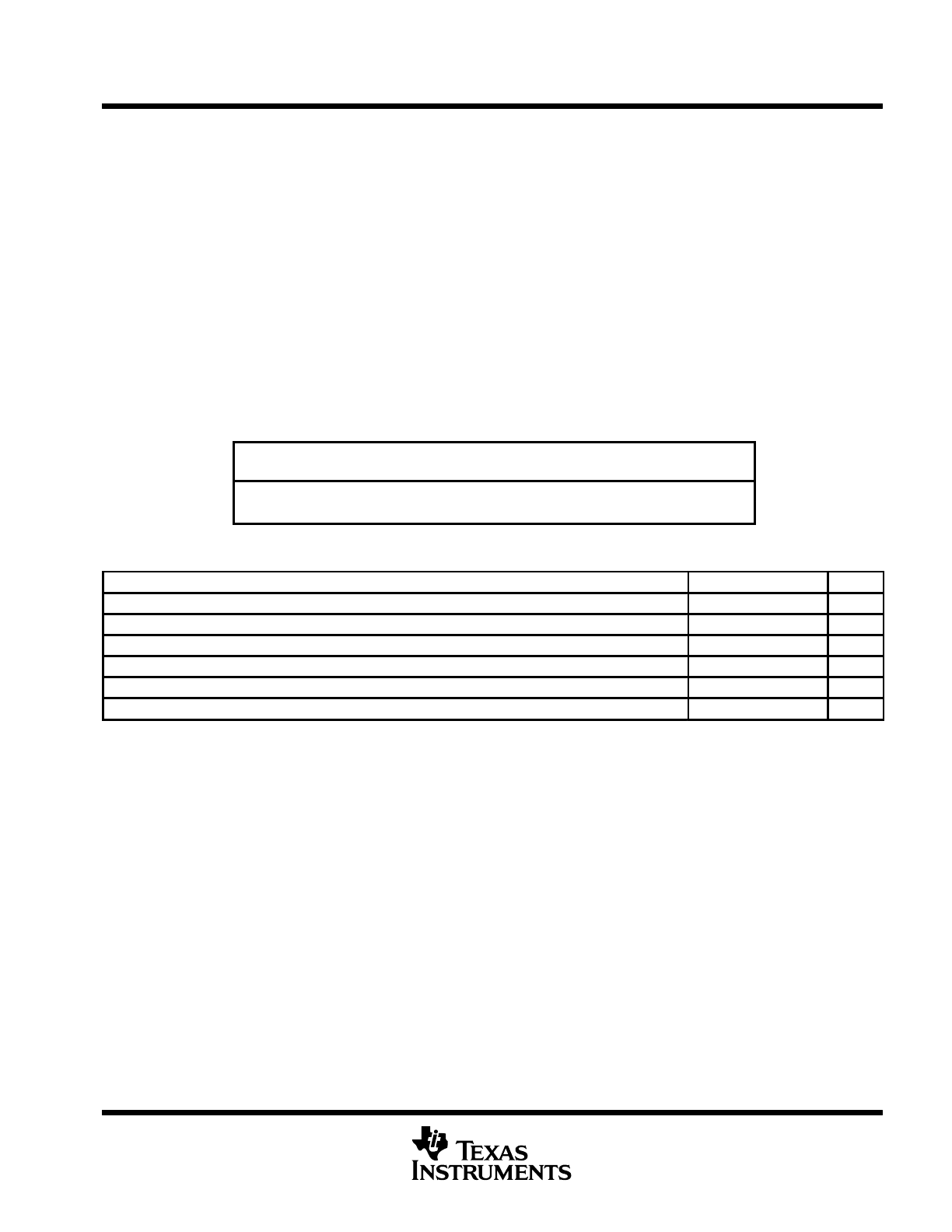
DISSIPATION RATING TABLE
PACKAGE
TA
≤
25
°
C
DERATING FACTOR
TA = 70
°
C
PACKAGE
A
POWER RATING
ABOVE TA = 25
°
C
A
POWER RATING
D
950 mW
7.6 mW/
°
C
608 mW
N
1150 mW
9.2 mW/
°
C
736 mW
recommended operating conditions
MIN
NOM
MAX
UNIT
Supply voltage, VCC
4.75
5
5.25
V
Common-mode input voltage, VIC
±
7
V
Differential input voltage, VID
±
6
V
High-level enable input voltage, VIH
2
V
Low-level enable input voltage, VIL
0.8
V
Operating free-air temperature, TA
0
70
°
C
MC3486
QUADRUPLE DIFFERENTIAL LINE RECEIVER
WITH 3-STATE OUTPUTS
SLLS097B – JUNE 1980 – REVISED MAY 1995
4
POST OFFICE BOX 655303
•
DALLAS, TEXAS 75265
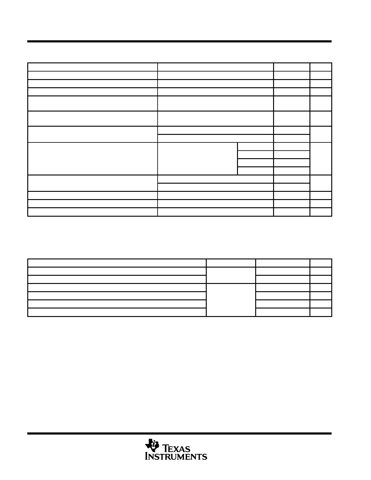
electrical characteristics over recommended ranges of common-mode input voltage, supply
voltage, and operating free-air temperature (unless otherwise noted)
PARAMETER
TEST CONDITIONS
MIN
MAX
UNIT
VIT +
Differential input high-threshold voltage
VO = 2.7 V,
IO = – 0.4 mA
0.2
V
VIT –
Differential input low-threshold voltage
VO = 0.5 V,
IO = – 8 mA
– 0.2†
V
VIK
Enable-input clamp voltage
II = – 10 mA
– 1.5
V
VOH
High level output voltage
VID = 0.4 V, IO = – 0.4 mA,
2 7
V
VOH
High-level output voltage
ID
,
O
,
See Note 3 and Figure 1
2.7
V
VOL
Low level output voltage
VID = – 0.4 V, IO = 8 mA,
0 5
V
VOL
Low-level output voltage
ID
, O
,
See Note 3 and Figure 1
0.5
V
IOZ
High impedance state output current
VIL = 0.8 V,
VID = – 3 V,
VO = 2.7 V
40
µ
A
IOZ
High-impedance-state output current
VIL = 0.8 V,
VID = 3 V,
VO = 0.5 V
– 40
µ
A
VI = – 10 V
– 3.25
IIB
Differential input bias current
VCC = 0 V or 5.25 V,
VI = – 3 V
–1.5
mA
IIB
Differential-input bias current
CC
,
Other inputs at 0 V
VI = 3 V
1.5
mA
VI = 10 V
3.25
IIH
High level enable input current
VI = 5.25 V
100
µ
A
IIH
High-level enable input current
VI = 2.7 V
20
µ
A
IIL
Low-level enable input current
VI = – 0.5 V
– 100
µ
A
IOS
Short-circuit output current
VID = 3 V,
VO = 0,
See Note 4
– 15
– 100
mA
ICC
Supply current
VIL = 0
85
mA
† The algebraic convention, in which the least positive (most negative) limit is designated as minimum, is used in this data sheet for threshold
voltages only.
NOTES:
3. Refer to ANSI Standards EIA/TIA-422-B and EIA/TIA-423-B for exact conditions.
4. Only one output should be shorted at a time.
switching characteristics, V
CC
= 5 V, C
L
= 15 pF, T
A
= 25
°
C
PARAMETER
TEST CONDITIONS
MIN
TYP
MAX
UNIT
tPHL
Propagation delay time, high- to low-level output
See Figure 2
28
35
ns
tPLH
Propagation delay time, low- to high-level output
See Figure 2
27
30
ns
tPZH
Output enable time to high level
13
30
ns
tPZL
Output enable time to low level
See Figure 3
20
30
ns
tPHZ
Output disable time from high level
See Figure 3
26
35
ns
tPLZ
Output disable time from low level
27
35
ns
MC3486
QUADRUPLE DIFFERENTIAL LINE RECEIVER
WITH 3-STATE OUTPUTS
SLLS097B – JUNE 1980 – REVISED MAY 1995
5
POST OFFICE BOX 655303
•
DALLAS, TEXAS 75265
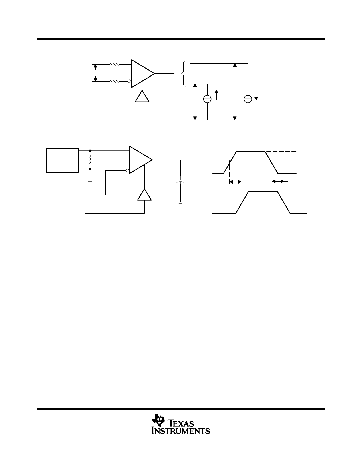
PARAMETER MEASUREMENT INFORMATION
500
Ω
VID
2 V
VOL
IOL
(+)
IOH
(–)
VOH
500
Ω
Figure 1. V
OH
, V
OL
Generator
(see Note A)
51
Ω
Output
CL = 15 pF
(see Note B)
1.5 V
2 V
Input 1.5 V
tPLH
tPHL
1.3 V
Output
VOL
VOH
0 V
3 V
1.3 V
1.5 V
TEST CIRCUIT
VOLTAGE WAVEFORMS
NOTES: A. The input pulse is supplied by a generator having the following characteristics: PRR
≤
1 MHz, duty cycle = 50%, tr
≤
6 ns,
tf
≤
6 ns.
B. CL includes probe and stray capacitance.
Figure 2. Test Circuit and Voltage Waveforms
MC3486
QUADRUPLE DIFFERENTIAL LINE RECEIVER
WITH 3-STATE OUTPUTS
SLLS097B – JUNE 1980 – REVISED MAY 1995
6
POST OFFICE BOX 655303
•
DALLAS, TEXAS 75265
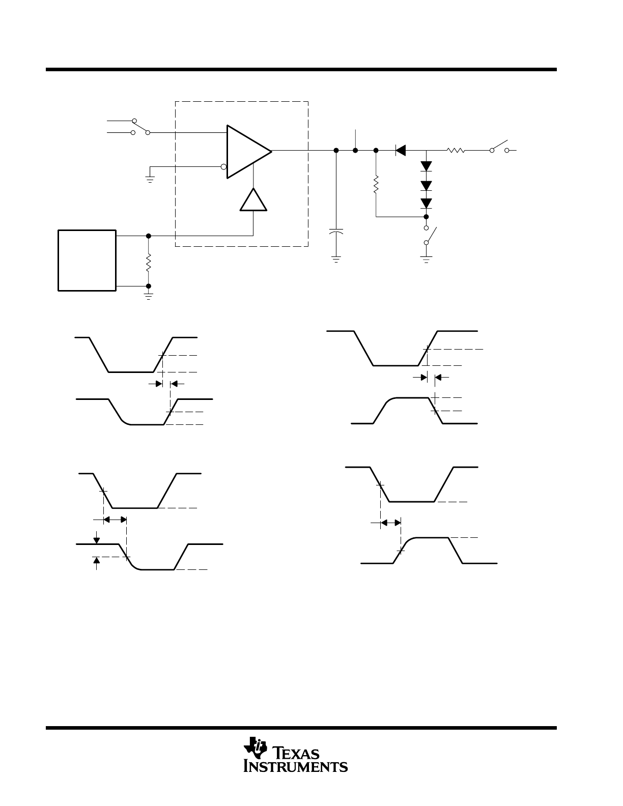
PARAMETER MEASUREMENT INFORMATION
tPZH
3 V
1.5 V
0 V
VOH
1.3 V
Input
Output
tPZH
SW1 to 1.5 V
SW2 Open
SW3 Closed
SW3 Closed
SW2 Closed
SW1 to 1.5 V
tPHZ
tPHZ
1.3 V
VOH
0 V
3 V
0.5 V
SW3 Open
SW2 Closed
SW1 to – 1.5 V
tPZL
tPZL
0 V
1.5 V
3 V
0 V
tPLZ
tPLZ
SW1 to – 1.5 V
SW2 Closed
SW3 Closed
4.5 V
1.5 V
VOL
3 V
1.3 V
0.5 V
VOL
1.5 V
1.5 V
Input
Output
Input
Output
Input
Output
NOTES: A. The input pulse is supplied by a generator having the following characteristics: PRR
≤
1 MHz, duty cycle = 50%, tr
≤
6 ns,
tf
≤
6 ns.
B. CL includes probe and stray capacitance.
C. All diodes are 1N916 or equivalent.
Generator
(see Note A)
51
Ω
– 1.5 V
1.5 V
SW1
CL = 15 pF
(see Note B)
5 k
Ω
See Note C
SW3
SW2
5 V
2 k
Ω
Output
TEST CIRCUIT
Figure 3. Test Circuit and Voltage Waveforms

IMPORTANT NOTICE
Texas Instruments and its subsidiaries (TI) reserve the right to make changes to their products or to discontinue
any product or service without notice, and advise customers to obtain the latest version of relevant information
to verify, before placing orders, that information being relied on is current and complete. All products are sold
subject to the terms and conditions of sale supplied at the time of order acknowledgment, including those
pertaining to warranty, patent infringement, and limitation of liability.
TI warrants performance of its products to the specifications applicable at the time of sale in accordance with
TI’s standard warranty. Testing and other quality control techniques are utilized to the extent TI deems necessary
to support this warranty. Specific testing of all parameters of each device is not necessarily performed, except
those mandated by government requirements.
Customers are responsible for their applications using TI components.
In order to minimize risks associated with the customer’s applications, adequate design and operating
safeguards must be provided by the customer to minimize inherent or procedural hazards.
TI assumes no liability for applications assistance or customer product design. TI does not warrant or represent
that any license, either express or implied, is granted under any patent right, copyright, mask work right, or other
intellectual property right of TI covering or relating to any combination, machine, or process in which such
products or services might be or are used. TI’s publication of information regarding any third party’s products
or services does not constitute TI’s approval, license, warranty or endorsement thereof.
Reproduction of information in TI data books or data sheets is permissible only if reproduction is without
alteration and is accompanied by all associated warranties, conditions, limitations and notices. Representation
or reproduction of this information with alteration voids all warranties provided for an associated TI product or
service, is an unfair and deceptive business practice, and TI is not responsible nor liable for any such use.
Resale of TI’s products or services with
statements different from or beyond the parameters stated by TI for
that product or service voids all express and any implied warranties for the associated TI product or service,
is an unfair and deceptive business practice, and TI is not responsible nor liable for any such use.
Also see: Standard Terms and Conditions of Sale for Semiconductor Products. www.ti.com/sc/docs/stdterms.htm
Mailing Address:
Texas Instruments
Post Office Box 655303
Dallas, Texas 75265
Copyright
2001, Texas Instruments Incorporated