
©2001 Fairchild Semiconductor Corporation
www.fairchildsemi.com
Rev. 1.0.1
Features
• Low input bias current : 250nA (Max)
• Low input offset current : 50nA (Max)
• Differential Input Voltage :
±
30V
• Power supply voltage : single 5.0V supply to
±
15V.
• Offset voltage null capability.
• Strobe capability.
Description
The LM311 series is a monolithic, low input current voltage
comparator. The device is also designed to operate from dual
or single supply voltage.
8-DIP
8-SOP
1
1
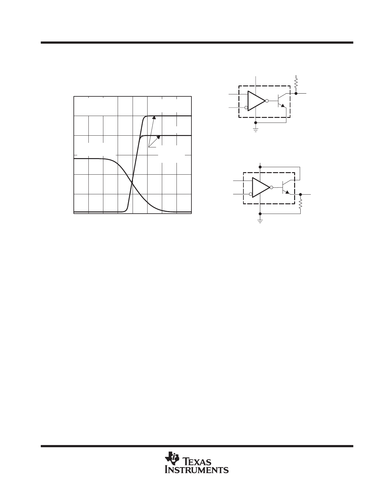
Internal Block Diagram
LM311
Single Comparator
LM311
2
Schematic Diagram
Absolute Maximum Ratings
Parameter
Symbol
Value
Unit
Total Supply Voltage
V
CC
36
V
Output to Negative Supply Voltage LM311
V
O
- V
EE
40
V
Ground to Negative voltage
V
EE
-30
V
Differential Input Voltage
V
I(DIFF)
30
V
Input Voltage
V
I
±
15
V
Output Short Circuit Duration
-
10
sec
Power Dissipation
P
D
500
mW
Operating Temperature Range
T
OPR
0 ~ +70
°
C
Storage Temperature Range
T
STG
- 65 ~ +150
°
C
LM311
3
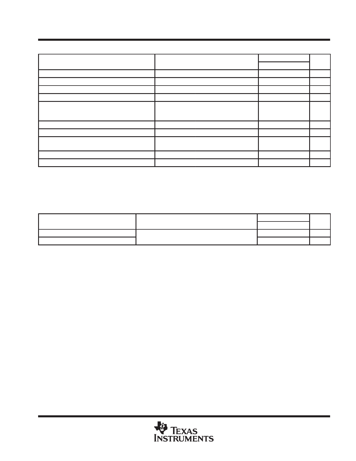
Electrical Characteristics
(V
CC
= 15V, T
A
= 25
°
C, unless otherwise specified)
Notes :
1. 0
≤
T
A
≤
+70
°
C
2. The response time specified is for a 100mV input step with 5mV over drive.
Parameter
Symbol
Conditions
Min.
Typ.
Max.
Unit
Input Offset Voltage
V
IO
R
S
≤
50K
Ω
-
1.0
7.5
mV
Note 1
-
-
10
Input Offset Current
I
IO
-
6
50
nA
Note 1
-
-
70
Input Bias Current
I
BIAS
-
100
250
nA
Note 1
-
-
300
Voltage Gain
G
V
-
40
200
-
V/mV
Response Time
T
RES
Note 2
-
200
-
ns
Saturation Voltage
V
SAT
I
O
=50mA, V
I
≤
-10mV
-
0.75
1.5
V
V
CC
≥
4.5V, V
EE
=0V
I
O
=8mA, V
I
≤
-10mV, Note 1
-
0.23
0.4
Strobe “ON” Current
I
STR(ON)
-
-
3
-
mA
Output Leakage Current
I
SINK
I
STR
=3mA, V
I
≥
10mV
V
O
=15V, V
CC
=±15V
-
0.2
50
nA
Input Voltage Range
V
I(R)
Note 1
-14.5
to
13.0
-14.7
to
13.8
-
V
Positive Supply Current
I
CC
-
-
3.0
7.5
mA
Negative Supply Current
I
EE
-
-
-2.2
-5.0
mA
Strobe Current
I
STR
-
-
3
-
mA
LM311
4
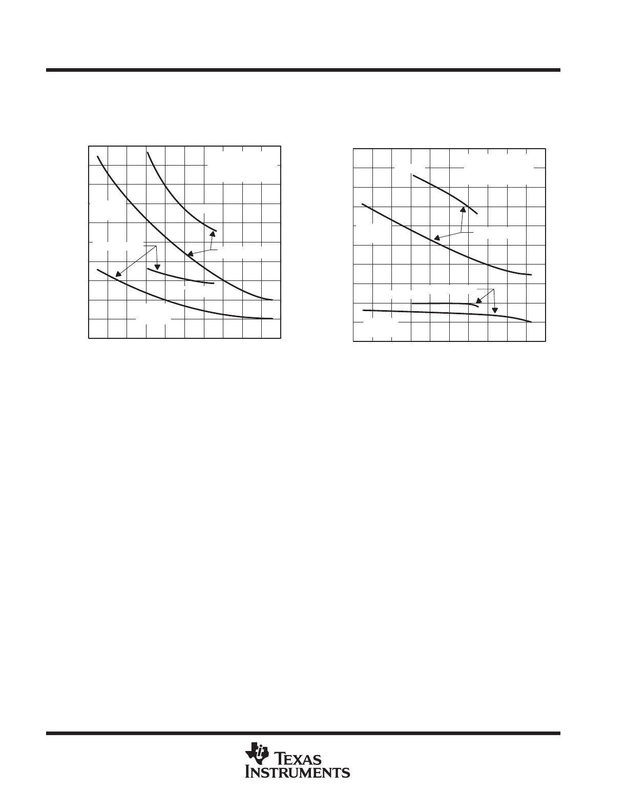
Typical Performance Characteristics
Figure 1. Input Bias Current vs Temperature
Figure 2. Input Offset Current vs Temperature
Figure 3. Offset Voltage vs Input Resistance
Figure 4. Input Bias Current vs
Differential input voltage
Figure 5. Common Mode Limits vs Temperature
Figure 6. Output Voltage vs
Differential input voltage
LM311
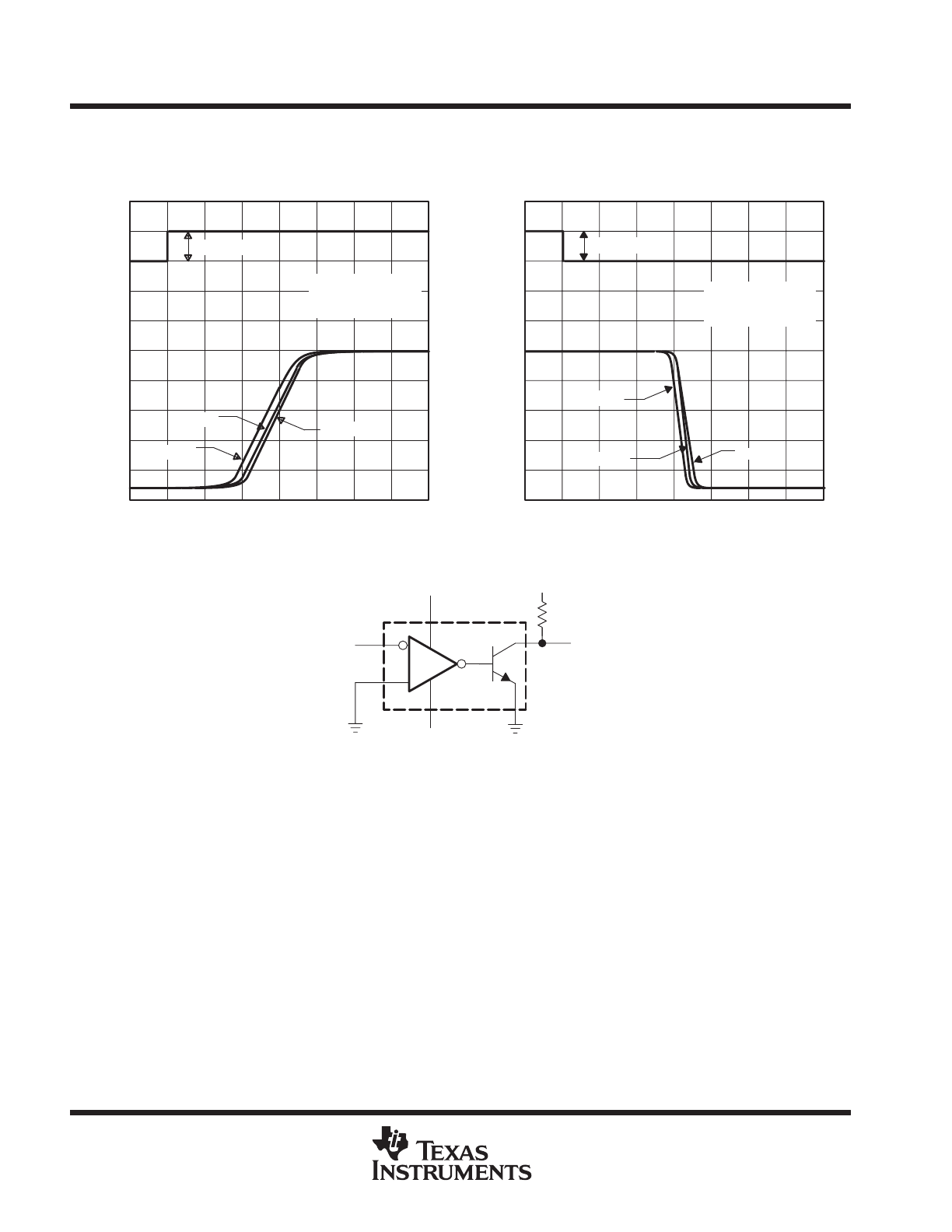
5
Typical Performance Characteristics (continued)
Figure 7. Saturation voltage vs Current
Figure 8. Supply Current vs Temperature
Figure 9. Leakage Current vs Temperature
Figure 10. Supply Current vs Supply Voltage
Figure 11. Current Saturation Voltage
Figure 12. Output Limiting Characterstics
LM311
6
Mechanical Dimensions
Package
6.40
±
0.20
3.30
±
0.30
0.130
±
0.012
3.40
±
0.20
0.134
±
0.008
#1
#4
#5
#8
0.252
±
0.008
9.20
±
0.20
0.79
2.54
0.100
0.031
()
0.46
±
0.10
0.018
±
0.004
0.060
±
0.004
1.524
±
0.10
0.362
±
0.008
9.60
0.378
MAX
5.08
0.200
0.33
0.013
7.62
0~15
°
0.300
MAX
MIN
0.25
+0.10
–0.05
0.010
+0.004
–0.002
8-DIP
LM311
7
Mechanical Dimensions
(Continued)
Package
4.92
±
0.20
0.194
±
0.008
0.41
±
0.10
0.016
±
0.004
1.27
0.050
5.72
0.225
1.55
±
0.20
0.061
±
0.008
0.1~0.25
0.004~0.001
6.00
±
0.30
0.236
±
0.012
3.95
±
0.20
0.156
±
0.008
0.50
±
0.20
0.020
±
0.008
5.13
0.202
MAX
#1
#4
#5
0~8
°
#8
0.56
0.022
()
1.80
0.071
MAX0.10
MAX0.004
MAX
MIN
+
0.10
-0.05
0.15
+
0.004
-0.002
0.006
8-SOP
LM311
8
Ordering Information
Product Number
Package
Operating Temperature
LM311N
8-DIP
0 ~ +70
°
C
LM311M
8-SOP
LM311
9
LM311
6/1/01 0.0m 001
Stock#DSxxxxxxxx
2001 Fairchild Semiconductor Corporation
LIFE SUPPORT POLICY
FAIRCHILD’S PRODUCTS ARE NOT AUTHORIZED FOR USE AS CRITICAL COMPONENTS IN LIFE SUPPORT DEVICES
OR SYSTEMS WITHOUT THE EXPRESS WRITTEN APPROVAL OF THE PRESIDENT OF FAIRCHILD SEMICONDUCTOR
CORPORATION. As used herein:
1. Life support devices or systems are devices or systems
which, (a) are intended for surgical implant into the body,
or (b) support or sustain life, and (c) whose failure to
perform when properly used in accordance with
instructions for use provided in the labeling, can be
reasonably expected to result in a significant injury of the
user.
2. A critical component in any component of a life support
device or system whose failure to perform can be
reasonably expected to cause the failure of the life support
device or system, or to affect its safety or effectiveness.
www.fairchildsemi.com
DISCLAIMER
FAIRCHILD SEMICONDUCTOR RESERVES THE RIGHT TO MAKE CHANGES WITHOUT FURTHER NOTICE TO ANY
PRODUCTS HEREIN TO IMPROVE RELIABILITY, FUNCTION OR DESIGN. FAIRCHILD DOES NOT ASSUME ANY
LIABILITY ARISING OUT OF THE APPLICATION OR USE OF ANY PRODUCT OR CIRCUIT DESCRIBED HEREIN; NEITHER
DOES IT CONVEY ANY LICENSE UNDER ITS PATENT RIGHTS, NOR THE RIGHTS OF OTHERS.
LM111, LM211, LM311
DIFFERENTIAL COMPARATORS WITH STROBES
SLCS007C – SEPTEMBER 1973 – REVISED OCTOBER 2000
1
POST OFFICE BOX 655303
•
DALLAS, TEXAS 75265
D
Fast Response Times
D
Strobe Capability
D
Maximum Input Bias Current . . . 300 nA
D
Maximum Input Offset Current . . . 70 nA
D
Can Operate From Single 5-V Supply
D
Designed to Be Interchangeable With
National Semiconductor LM111, LM211, and
LM311
D
Available in Q-Temp Automotive
– High Reliability Automotive Applications
– Configuration Control/Print Support
– Qualification to Automotive Standards
description
The LM111, LM211, and LM311 are single
high-speed voltage comparators. These devices
are designed to operate from a wide range of
power-supply voltages, including
±
15-V supplies
for operational amplifiers and 5-V supplies for
logic systems. The output levels are compatible
with most TTL and MOS circuits. These
comparators are capable of driving lamps or
relays and switching voltages up to 50 V at 50 mA.
All inputs and outputs can be isolated from system
ground. The outputs can drive loads referenced to
ground, V
CC+
or V
CC–
. Offset balancing and
strobe capabilities are available, and the outputs
can be wire-OR connected. If the strobe is low, the
output is in the off state, regardless of the
differential input.
The LM111 is characterized for operation over the full military temperature range of –55
°
C to 125
°
C. The LM211
is characterized for operation from –40
°
C to 85
°
C. The LM211Q is characterized for operation over the full
automotive range of –40
°
C to 125
°
C. The LM311 is characterized for operation from 0
°
C to 70
°
C.
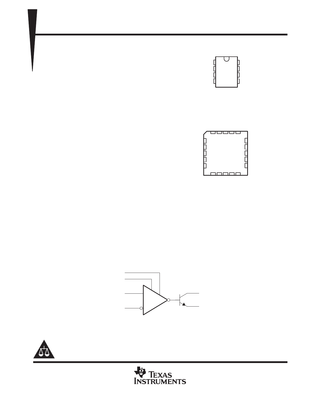
functional block diagram
BAL/STRB
COL OUT
IN–
IN+
BALANCE
EMIT OUT
+
–
Please be aware that an important notice concerning availability, standard warranty, and use in critical applications of
Texas Instruments semiconductor products and disclaimers thereto appears at the end of this data sheet.
Copyright
2000, Texas Instruments Incorporated
PRODUCTION DATA information is current as of publication date.
Products conform to specifications per the terms of Texas Instruments
standard warranty. Production processing does not necessarily include
testing of all parameters.
1
2
3
4
8
7
6
5
EMIT OUT
IN+
IN–
V
CC–
V
CC+
COL OUT
BAL/STRB
BALANCE
LM111 . . . JG PACKAGE
LM211, LM311 . . . D, P, OR PW PACKAGE
(TOP VIEW)
3
2
1 20 19
9 10 11 12 13
4
5
6
7
8
18
17
16
15
14
NC
COL OUT
NC
BAL/STRB
NC
NC
IN+
NC
IN–
NC
LM111 . . . FK PACKAGE
(TOP VIEW)
NC
EMIT
OUT
NC
BALANCE
NC
NC
NC
NC
CC–
V
CC+
V
NC – No internal connection
On products compliant to MIL-PRF-38535, all parameters are tested
unless otherwise noted. On all other products, production
processing does not necessarily include testing of all parameters.
LM111, LM211, LM311
DIFFERENTIAL COMPARATORS WITH STROBES
SLCS007C – SEPTEMBER 1973 – REVISED OCTOBER 2000
2
POST OFFICE BOX 655303
•
DALLAS, TEXAS 75265
AVAILABLE OPTIONS
PACKAGED DEVICES
TA
VIO max
AT 25
°
C
PLASTIC
SMALL
OUTLINE
(D)
CERAMIC
CHIP
CARRIER
(FK)
CERAMIC
DIP
(JG)
PLASTIC
DIP
(P)
PLASTIC
TSSOP
(PW)
CHIP
FORM
0
°
C to 70
°
C
7.5 mV
LM311D
LM311P
LM311PWR
–40
°
C to 85
°
C
3 mV
LM211D
LM211P
LM311Y
–40
°
C to 125
°
C
3 mV
LM211QD
LM311Y
–55
°
C to 125
°
C
3 mV
LM111FK
LM111JG
The D package also is available taped and reeled. Add the suffix R to device type (e.g., LM311DR). The PW package
is only available taped and reeled. Chip forms are tested at 25
°
C only.
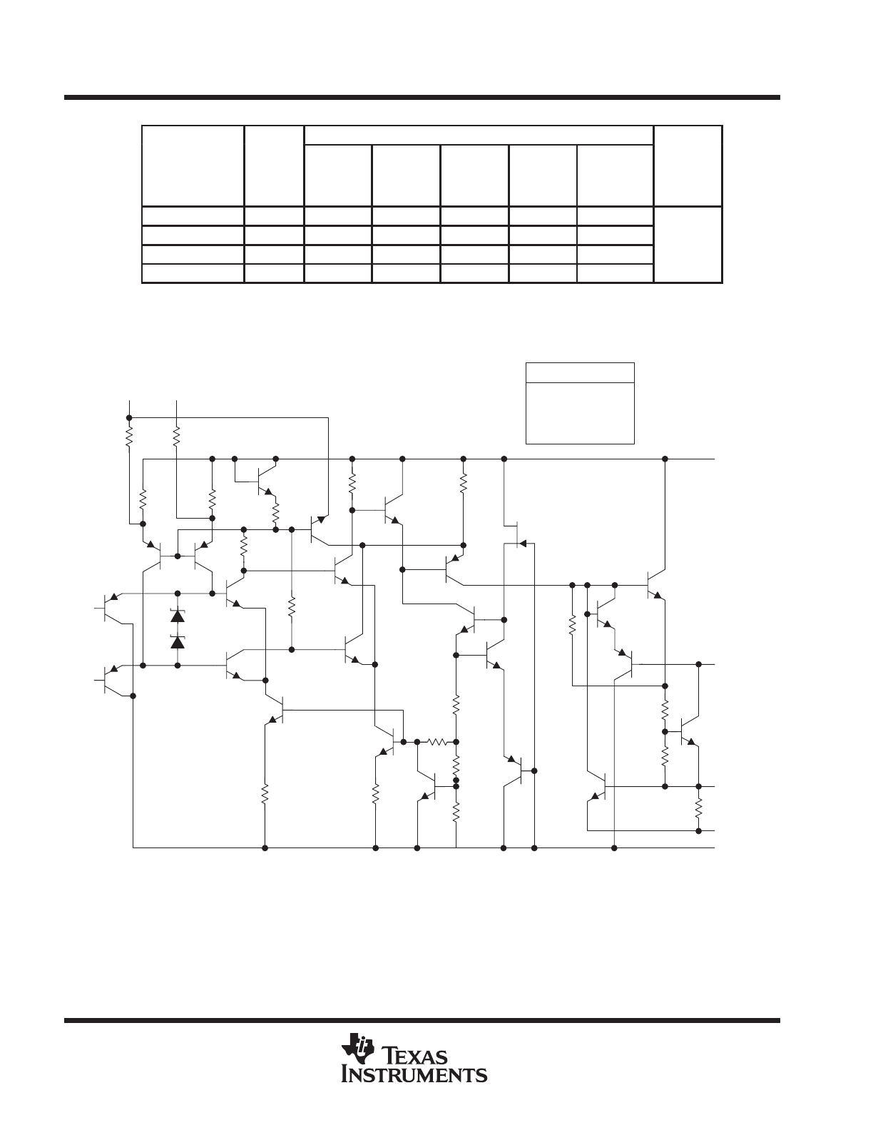
schematic
All resistor values shown are nominal.
BAL/STRB BALANCE
IN+
IN–
450
Ω
450
Ω
2.4
k
Ω
1.2 k
Ω
70
Ω
2.4
k
Ω
1.2 k
Ω
60
Ω
400
Ω
450
Ω
2 k
Ω
200
Ω
250
Ω
600
Ω
130
Ω
4
Ω
4 k
Ω
VCC+
VCC–
EMIT OUT
COL OUT
750
Ω
600
Ω
Component Count
Resistors
20
Diodes
2
EPI FET
1
Transistors 22
LM111, LM211, LM311
DIFFERENTIAL COMPARATORS WITH STROBES
SLCS007C – SEPTEMBER 1973 – REVISED OCTOBER 2000
3
POST OFFICE BOX 655303
•
DALLAS, TEXAS 75265
absolute maximum ratings over operating free-air temperature range (unless otherwise noted)
†
Supply voltage: V
CC+
(see Note 1)
18 V
. . . . . . . . . . . . . . . . . . . . . . . . . . . . . . . . . . . . . . . . . . . . . . . . . . . . . . . . . . .
V
CC–
(see Note 1)
–18 V
. . . . . . . . . . . . . . . . . . . . . . . . . . . . . . . . . . . . . . . . . . . . . . . . . . . . . . . . . .
V
CC+
– V
CC–
36 V
. . . . . . . . . . . . . . . . . . . . . . . . . . . . . . . . . . . . . . . . . . . . . . . . . . . . . . . . . . . . . . .
Differential input voltage, V
ID
(see Note 2)
±
30 V
. . . . . . . . . . . . . . . . . . . . . . . . . . . . . . . . . . . . . . . . . . . . . . . . . . .
Input voltage, V
I
(either input, see Notes 1 and 3)
±
15 V
. . . . . . . . . . . . . . . . . . . . . . . . . . . . . . . . . . . . . . . . . . . . .
Voltage from emitter output to V
CC–
30
V
. . . . . . . . . . . . . . . . . . . . . . . . . . . . . . . . . . . . . . . . . . . . . . . . . . . . . . . . . .
Voltage from collector output to V
CC–
: LM111 50
V
. . . . . . . . . . . . . . . . . . . . . . . . . . . . . . . . . . . . . . . . . . . . . . . . .
LM211 50
V
. . . . . . . . . . . . . . . . . . . . . . . . . . . . . . . . . . . . . . . . . . . . . . . . .
LM211Q 50
V
. . . . . . . . . . . . . . . . . . . . . . . . . . . . . . . . . . . . . . . . . . . . . . .
LM311 40
V
. . . . . . . . . . . . . . . . . . . . . . . . . . . . . . . . . . . . . . . . . . . . . . . . .
Duration of output short circuit (see Note 4)
10 s
. . . . . . . . . . . . . . . . . . . . . . . . . . . . . . . . . . . . . . . . . . . . . . . . . . .
Continuous total dissipation
See Dissipation Rating Table
. . . . . . . . . . . . . . . . . . . . . . . . . . . . . . . . . . . . . . . . . . .
Package thermal impedance,
θ
JA
(see Note 5): D package
97
°
C/W
. . . . . . . . . . . . . . . . . . . . . . . . . . . . . . . . . . .
P package
85
°
C/W
. . . . . . . . . . . . . . . . . . . . . . . . . . . . . . . . . . .
PW package
149
°
C/W
. . . . . . . . . . . . . . . . . . . . . . . . . . . . . . . .
Case temperature for 60 seconds: FK package
260
°
C
. . . . . . . . . . . . . . . . . . . . . . . . . . . . . . . . . . . . . . . . . . . . . .
Lead temperature 1,6 mm (1/16 inch) from case for 10 seconds: J or JG package
300
°
C
. . . . . . . . . . . . . . . .
Lead temperature 1,6 mm (1/16 inch) from case for 60 seconds: D, P, or PW package
260
°
C
. . . . . . . . . . . .
Storage temperature range, T
stg
–65
°
C to 150
°
C
. . . . . . . . . . . . . . . . . . . . . . . . . . . . . . . . . . . . . . . . . . . . . . . . . . .
† Stresses beyond those listed under “absolute maximum ratings” may cause permanent damage to the device. These are stress ratings only, and
functional operation of the device at these or any other conditions beyond those indicated under “recommended operating conditions” is not
implied. Exposure to absolute-maximum-rated conditions for extended periods may affect device reliability.
NOTES:
1. All voltage values, unless otherwise noted, are with respect to the midpoint between VCC+ and VCC–.
2. Differential voltages are at IN+ with respect to IN–.
3. The magnitude of the input voltage must never exceed the magnitude of the supply voltage or
±
15 V, whichever is less.
4. The output may be shorted to ground or either power supply.
5. The package thermal impedance is calculated in accordance with JESD 51-7.
DISSIPATION RATING TABLE
PACKAGE
TA
≤
25
°
C
POWER RATING
DERATING
FACTOR
DERATE
ABOVE TA
TA = 70
°
C
POWER RATING
TA = 85
°
C
POWER RATING
TA = 125
°
C
POWER RATING
FK
500 mW
11.0 mW/
°
C
105
°
C
500 mW
500 mW
275 mW
JG
500 mW
8.4 mW/
°
C
90
°
C
500 mW
500 mW
210 mW
recommended operating conditions
MIN
MAX
UNIT
Supply voltage, VCC+ – VCC–
3.5
30
V
Input voltage (|VCC
±
|
≤
15 V)
VCC–+0.5
VCC+–1.5
V
LM111
–55
125
Operating free air temperature range TA
LM211
–40
85
°
C
Operating free-air temperature range, TA
LM211Q
–40
125
°
C
LM311
0
70
LM111, LM211, LM311
DIFFERENTIAL COMPARATORS WITH STROBES
SLCS007C – SEPTEMBER 1973 – REVISED OCTOBER 2000
4
POST OFFICE BOX 655303
•
DALLAS, TEXAS 75265
electrical characteristics at specified free-air temperature, V
CC
±
=
±
15 V (unless otherwise noted)
PARAMETER
TEST CONDITIONS
TA†
LM111
LM211
LM211Q
LM311
UNIT
MIN
TYP‡
MAX
MIN
TYP‡
MAX
VIO
Input offset voltage
See Note 6
25
°
C
0.7
3
2
7.5
mV
VIO
Input offset voltage
See Note 6
Full range
4
10
mV
IIO
Input offset current
See Note 6
25
°
C
4
10
6
50
nA
IIO
Input offset current
See Note 6
Full range
20
70
nA
IIB
Input bias current
VO = 1 V to 14 V
25
°
C
75
100
100
250
nA
IIB
Input bias current
VO = 1 V to 14 V
Full range
150
300
nA
IIL(S)
Low-level
strobe current
(see Note 7)
V(strobe) = 0.3 V,
VID
≤
–10 mV
25
°
C
–3
–3
mA
VICR
Common-mode
input voltage range
Full range
13
to
–14.5
13.8
to
–14.7
13
to
–14.5
13.8
to
–14.7
V
AVD
Large-signal
differential voltage
amplification
VO = 5 V to 35 V,
RL = 1 k
Ω
25
°
C
40
200
40
200
V/mV
High-level
(
ll
t )
I(strobe) = –3 mA, VOH = 35 V,
25
°
C
0.2
10
nA
IOH
(collector)
output leakage
(strobe)
,
VID = 5 mV
OH
,
Full range
0.5
µ
A
out ut leakage
current
VID = 5 mV,
VOH = 35 V
25
°
C
0.2
50
nA
IOL = 50 mA
VID = –5 mV
25
°
C
0.75
1.5
Low-level
IOL = 50 mA
VID = –10 mV
25
°
C
0.75
1.5
VOL
(collector-to-emitter)
output voltage
VCC+ = 4.5 V,
VCC
0
VID = –6 mV
Full range
0.23
0.4
V
out ut voltage
VCC– = 0,
IOL = 8 mA
VID = –10 mV
Full range
0.23
0.4
ICC+
Supply current
from VCC+,
output low
VID = –10 mV,
No load
25
°
C
5.1
6
5.1
7.5
mA
ICC–
Supply current
from VCC–,
output high
VID = 10 mV,
No load
25
°
C
–4.1
–5
–4.1
–5
mA
† Unless otherwise noted, all characteristics are measured with BALANCE and BAL/STRB open and the emitter output grounded.
Full range for LM111 is –55
°
C to 125
°
C, for LM211 is –40
°
C to 85
°
C, for LM211Q is –40
°
C to 125
°
C, and for LM311 is 0
°
C to 70
°
C.
‡ All typical values are at TA = 25
°
C.
NOTES:
6. The offset voltages and offset currents given are the maximum values required to drive the collector output up to 14 V or down to
1 V with a pullup resistor of 7.5 k
Ω
to VCC+. These parameters actually define an error band and take into account the worst-case
effects of voltage gain and input impedance.
7. The strobe should not be shorted to ground; it should be current driven at –3 mA to –5 mA (see Figures 13 and 27).
switching characteristics, V
CC
±
=
±
15 V, T
A
= 25
°
C
PARAMETER
TEST CONDITIONS
LM111
LM211
LM211Q
LM311
UNIT
MIN
TYP
MAX
Response time, low-to-high-level output
RC = 500
Ω
to 5 V
CL = 5 pF
See Note 8
115
ns
Response time, high-to-low-level output
RC = 500
Ω
to 5 V,
CL = 5 pF,
See Note 8
165
ns
NOTE 8: The response time specified is for a 100-mV input step with 5-mV overdrive and is the interval between the input step function and the
instant when the output crosses 1.4 V.
LM111, LM211, LM311
DIFFERENTIAL COMPARATORS WITH STROBES
SLCS007C – SEPTEMBER 1973 – REVISED OCTOBER 2000
5
POST OFFICE BOX 655303
•
DALLAS, TEXAS 75265
electrical characteristics at V
CC
±
=
±
15 V, T
A
= 25
°
C (unless otherwise noted)
PARAMETER
TEST CONDITIONS†
LM311Y
UNIT
PARAMETER
TEST CONDITIONS†
MIN
TYP
MAX
UNIT
VIO
Input offset voltage
See Note 6
2
7.5
mV
IIO
Input offset current
See Note 6
6
50
nA
IIB
Input bias current
VO = 1 V to 14 V
100
250
nA
IIL(S)
Low-level strobe current (see Note 7)
V(strobe) = 0.3 V, VID
≤
–10 mV
–3
mA
VICR
Common-mode input voltage range
13
to
–14.5
13.8
to
–14.7
V
AVD
Large-signal differential voltage amplification
VO = 5 V to 35 V, RL = 1 k
Ω
40
200
V/mV
IOH
High-level (collector) output leakage current
Istrobe = –3 mA,
VID = 5 mV,
VOH = 35 V
0.2
50
nA
VOL
Low-level (collector-to-emitter)
output voltage
IOL = 50 mA,
VID = –10 mV
0.75
1.5
V
ICC+
Supply current from VCC+, output low
VID = –10 mV,
No load
5.1
7.5
mA
ICC–
Supply current from VCC–, output low
VID = 10 mV,
No load
–4.1
–5
mA
† Unless otherwise noted, all characteristics are measured with BALANCE and BAL/STRB open and the emitter output grounded.
NOTES:
6. The offset voltages and offset currents given are the maximum values required to drive the collector output up to 14 V or down to
1 V with a pullup resistor of 7.5 k
Ω
to VCC+. These parameters actually define an error band and take into account the worst-case
effects of voltage gain and input impedance.
7. The strobe should not be shorted to ground; it should be current driven at –3 mA to –5 mA (see Figures 13 and 27).
switching characteristics, V
CC
±
=
±
15 V, T
A
= 25
°
C
PARAMETER
TEST CONDITIONS
LM311Y
UNIT
PARAMETER
TEST CONDITIONS
MIN
TYP
MAX
UNIT
Response time, low-to-high-level output
RC = 500
Ω
to 5 V
CL = 5 pF
See Note 8
115
ns
Response time, high-to-low-level output
RC = 500
Ω
to 5 V,
CL = 5 pF,
See Note 8
165
ns
NOTE 8: The response time specified is for a 100-mV input step with 5-mV overdrive and is the interval between the input step function and the
instant when the output crosses 1.4 V.
LM111, LM211, LM311
DIFFERENTIAL COMPARATORS WITH STROBES
SLCS007C – SEPTEMBER 1973 – REVISED OCTOBER 2000
6
POST OFFICE BOX 655303
•
DALLAS, TEXAS 75265
TYPICAL CHARACTERISTICS
†
NOTE A: Condition 1 is with BALANCE and BAL/STRB open.
Condition 2 is with BALANCE and BAL/STRB connected
to VCC+.
Figure 1
10
8
4
2
0
18
6
–60 –40 –20
0
20
40
60
– Input Offset Current – nA
14
12
16
INPUT OFFSET CURRENT
vs
FREE-AIR TEMPERATURE
20
80
100 120 140
TA – Free-Air Temperature –
°
C
I
IO
LM311
Condition 2
Condition 1
LM111
LM211
LM111
LM211
LM311
VCC
±
=
±
15 V
VO = 1 V to 14 V
See Note A
NOTE A: Condition 1 is with BALANCE and BAL/STRB open.
Condition 2 is with BALANCE and BAL/STRB connected
to VCC+.
Figure 2
250
200
100
50
0
450
150
–60 –40 –20
0
20
40
60
– Input Bias Current – nA
350
300
400
500
80
100 120 140
I
IB
INPUT BIAS CURRENT
vs
FREE-AIR TEMPERATURE
TA – Free-Air Temperature –
°
C
LM311
LM311
LM111
LM211
Condition 2
VCC
±
=
±
15 V
VO = 1 V to 14 V
See Note A
LM111
LM211
Condition 1
† Data at high and low temperatures are applicable only within the rated operating free-air temperature ranges of the various devices.
LM111, LM211, LM311
DIFFERENTIAL COMPARATORS WITH STROBES
SLCS007C – SEPTEMBER 1973 – REVISED OCTOBER 2000
7
POST OFFICE BOX 655303
•
DALLAS, TEXAS 75265
TYPICAL CHARACTERISTICS
†
30
20
10
0
–1
–0.5
0
– Output V
oltage – V
40
50
VOLTAGE TRANSFER CHARACTERISTICS
60
0.5
1
V
O
VID – Differential Input Voltage – mV
VID
VCC+ = 30 V
1 k
Ω
Output
VCC–
VI = 50 V (LM111, LM211)
40 V (LM311)
VID
VCC+ = 30 V
600
Ω
VCC–
Output
COLLECTOR OUTPUT TRANSFER CHARACTERISTIC
TEST CIRCUIT FOR FIGURE 3
EMITTER OUTPUT TRANSFER CHARACTERISTIC
TEST CIRCUIT FOR FIGURE 3
Collector
Output
RL = 1 k
Ω
LM111
LM211
LM311
Emitter Output
RL = 600
Ω
VCC+ = 30 V
VCC– = 0
TA = 25
°
C
Figure 3
† Data at high and low temperatures are applicable only within the rated operating free-air temperature ranges of the various devices.
LM111, LM211, LM311
DIFFERENTIAL COMPARATORS WITH STROBES
SLCS007C – SEPTEMBER 1973 – REVISED OCTOBER 2000
8
POST OFFICE BOX 655303
•
DALLAS, TEXAS 75265
TYPICAL CHARACTERISTICS
Figure 4
4
3
1
0
0
50
100
150
200
250
5
t – Time – ns
300
350
2
Differential
Input V
oltage
– Output V
oltage – V
V
O
OUTPUT RESPONSE FOR
VARIOUS INPUT OVERDRIVES
100 mV
20 mV
2 mV
5 mV
VCC
±
=
±
15 V
RC = 500
Ω
to 5 V
TA = 25
°
C
Figure 5
4
3
1
0
0
50
100
150
200
250
5
t – Time – ns
OUTPUT RESPONSE FOR
VARIOUS INPUT OVERDRIVES
300
350
2
Differential
Input V
oltage
– Output V
oltage – V
V
O
20 mV
5 mV
2 mV
100 mV
VCC
±
=
±
15 V
RC = 500
Ω
to 5 V
TA = 25
°
C
VID
VCC+ = 15 V
500
Ω
VO
VCC– = –15 V
TEST CIRCUIT FOR FIGURES 4 AND 5
5 V
LM111, LM211, LM311
DIFFERENTIAL COMPARATORS WITH STROBES
SLCS007C – SEPTEMBER 1973 – REVISED OCTOBER 2000
9
POST OFFICE BOX 655303
•
DALLAS, TEXAS 75265
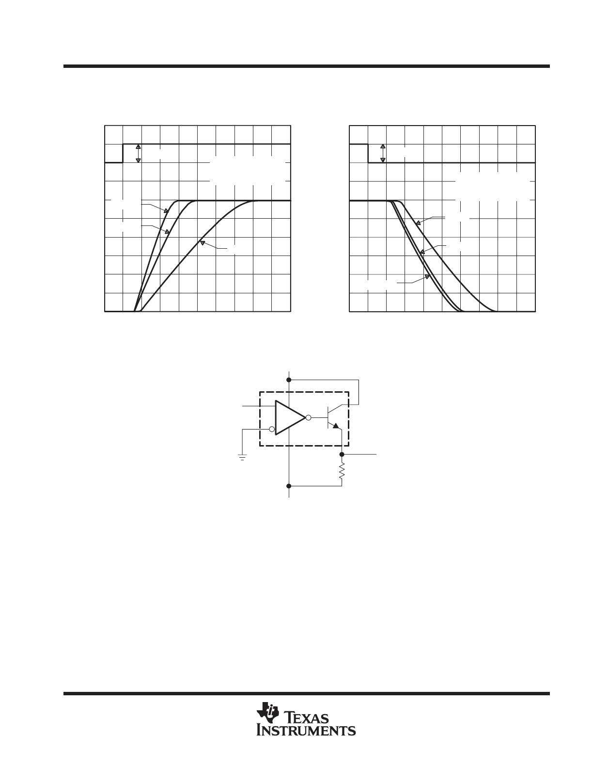
TYPICAL CHARACTERISTICS
Figure 6
5
0
–10
–15
0
0.2
0.4
0.6
0.8
1.0
10
t – Time – ns
1.2
1.4
–5
Differential
Input V
oltage
– Output V
oltage – V
V
O
OUTPUT RESPONSE FOR
VARIOUS INPUT OVERDRIVES
15
1.6
1.8
20 mV
100 mV
2 mV
5 mV
VCC
±
=
±
15 V
RE = 2 k
Ω
to –15 V
TA = 25
°
C
Figure 7
t – Time – ns
OUTPUT RESPONSE FOR
VARIOUS INPUT OVERDRIVES
Differential
Input V
oltage
– Output V
oltage – V
V
O
0
0.2
0.4
0.6
0.8
1.0
1.2
1.4 1.6
1.8
5
0
–10
–15
10
–5
15
20 mV
VCC
±
=
±
15 V
RE = 2 k
Ω
to –15 V
TA = 25
°
C
2 mV
5 mV
100 mV
VID
VCC+ = 15 V
RE = 2 k
Ω
VO
VCC– = –15 V
TEST CIRCUIT FOR FIGURES 6 AND 7
LM111, LM211, LM311
DIFFERENTIAL COMPARATORS WITH STROBES
SLCS007C – SEPTEMBER 1973 – REVISED OCTOBER 2000
10
POST OFFICE BOX 655303
•
DALLAS, TEXAS 75265
TYPICAL CHARACTERISTICS
Figure 8
60
40
20
0
0
5
10
– Output Current and Dissipation mA
80
100
120
15
I
O
VCC
±
=
±
15 V
t
≤
10 s
VID = –10 mV
TA = 25
°
C
VO – Output Voltage – V
140
160
300
200
100
0
– Output Dissipation – mW
400
500
600
P
O
700
800
OUTPUT CURRENT AND DISSIPATION
vs
OUTPUT VOLTAGE
PO (right scale)
IO (left scale)
Figure 9
3
2
1
0
0
5
10
4
5
6
15
TA = 25
°
C
No Load
VCC+ – Positive Supply Voltage – V
VID = –10 mV
POSITIVE SUPPLY CURRENT
vs
POSITIVE SUPPLY VOLTAGE
I
CC+
– Positive Supply Current – mA
VID = 10 mV
–3
–2
–1
0
0
–5
–10
–4
–5
–6
–15
NEGATIVE SUPPLY CURRENT
vs
NEGATIVE SUPPLY VOLTAGE
VCC– – Negative Supply Voltage – V
I
CC–
– Negative Supply Current – mA
VID = 10 mV or –10 mV
TA = 25
°
C
No Load
Figure 10
LM111, LM211, LM311
DIFFERENTIAL COMPARATORS WITH STROBES
SLCS007C – SEPTEMBER 1973 – REVISED OCTOBER 2000
11
POST OFFICE BOX 655303
•
DALLAS, TEXAS 75265
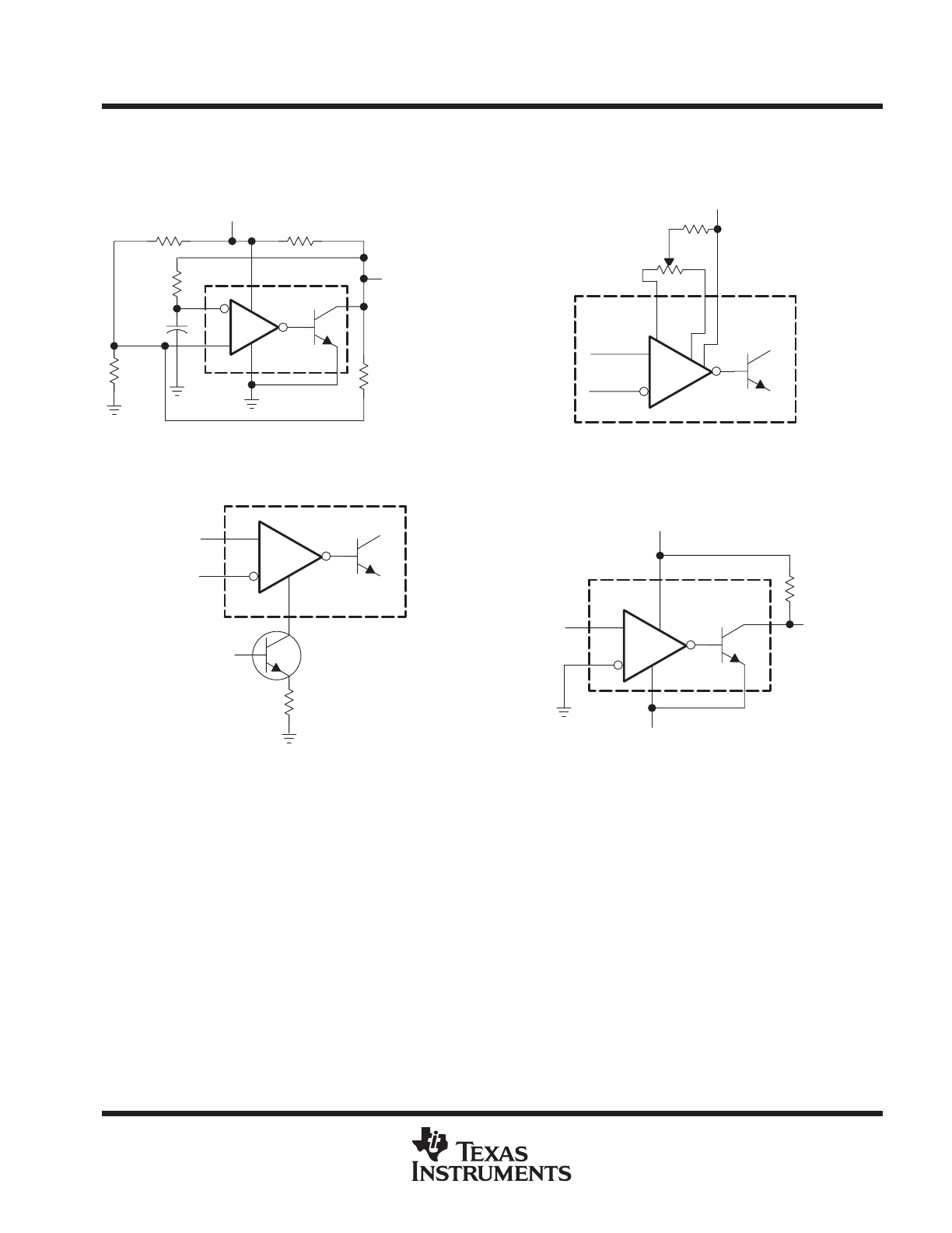
APPLICATION INFORMATION
Figure 11 through Figure 29 show various applications for the LM111, LM211, and LM311 comparators.
Figure 11. 100-kHz Free-Running Multivibrator
VCC+
39 k
Ω
1200 pF
20 k
Ω
1 k
Ω
10 k
Ω
20 k
Ω
Square Wave
Output
(fanout to two
Series 54 gates
or equivalent)
Figure 12. Offset Balancing
3 k
Ω
3 k
Ω
VCC+
BALANCE
BAL/
STRB
Figure 13. Strobing
1 k
Ω
BAL/STRB
TTL
Strobe
2N2222
Figure 14. Zero-Crossing Detector
VCC+
Input
VCC–
20 k
Ω
Output
LM111, LM211, LM311
DIFFERENTIAL COMPARATORS WITH STROBES
SLCS007C – SEPTEMBER 1973 – REVISED OCTOBER 2000
12
POST OFFICE BOX 655303
•
DALLAS, TEXAS 75265
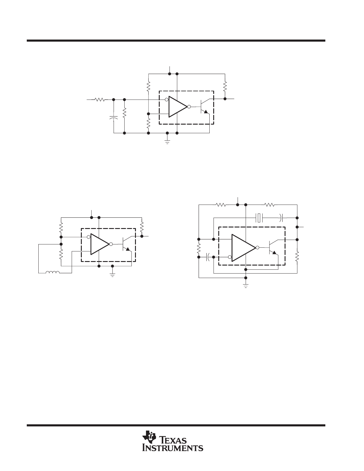
APPLICATION INFORMATION
† Resistor values shown are for a 0-to-30-V logic swing and a 15-V threshold.
‡ May be added to control speed and reduce susceptibility to noise spikes.
5 V
1 k
Ω
240 k
Ω
82 k
Ω
47 k
Ω
82 k
Ω
Output to TTL
Input†
‡
Figure 15. TTL Interface With High-Level Logic
Figure 16. Detector for Magnetic Transducer
5 V
2 k
Ω
4.5 k
Ω
1 k
Ω
Magnetic
Transducer
Output
to TTL
Figure 17. 100-kHz Crystal Oscillator
0.1
µ
F
50 k
Ω
VCC+
2 k
Ω
100 k
Ω
100 k
Ω
100 kHz
Output
10 pF
LM111, LM211, LM311
DIFFERENTIAL COMPARATORS WITH STROBES
SLCS007C – SEPTEMBER 1973 – REVISED OCTOBER 2000
13
POST OFFICE BOX 655303
•
DALLAS, TEXAS 75265
APPLICATION INFORMATION
Figure 18. Comparator and Solenoid Driver
Input
TIP30
22 k
Ω
Output
VCC+
Figure 19. Strobing Both Input and Output Stages
Simultaneously
†Typical input current is 50 pA with inputs strobed off.
VCC+
1 k
Ω
From D/A Network
0.1
µ
F
Sample
Analog
Input†
2N2222
TTL
Strobe
BAL/STRB
BALANCE
Figure 20. Low-Voltage Adjustable
Reference Supply
500
Ω
3.9 k
Ω
10 k
Ω
1.5
µ
F
+
VCC+
Output
2N2222
2N3708
1 k
Ω
Figure 21. Zero-Crossing Detector
Driving MOS Logic
3 k
Ω
3 k
Ω
VCC+ = 5 V
Input
10 k
Ω
VCC– = –10 V
Output
to MOS
BAL/
STRB
BALANCE
LM111, LM211, LM311
DIFFERENTIAL COMPARATORS WITH STROBES
SLCS007C – SEPTEMBER 1973 – REVISED OCTOBER 2000
14
POST OFFICE BOX 655303
•
DALLAS, TEXAS 75265
APPLICATION INFORMATION
† Adjust to set clamp level
3.9 k
Ω
30 k
Ω
†
1.5
µ
F
+
VCC+ = 5 V
Input
From
TTL
2N2222
2N3708
Output
510
Ω
1 k
Ω
1 k
Ω
2N2222
2N2222
2.2 k
Ω
1N914
1N914
2.7 k
Ω
Figure 22. Precision Squarer
5 k
Ω
0.01
µ
F
TTL
Output
1 k
Ω
1 k
Ω
1 k
Ω
100
Ω
From
TTL
Gate
50 k
Ω
TIL102
5 V
VCC+ = 5 V
Figure 23. Digital Transmission Isolator
1.5
µ
F
+
10 k
Ω
2 k
Ω
VCC+ = 15 V
TL081
Output
Input
1 M
Ω
VCC– = –15 V
–
+
Figure 24. Positive-Peak Detector
LM111, LM211, LM311
DIFFERENTIAL COMPARATORS WITH STROBES
SLCS007C – SEPTEMBER 1973 – REVISED OCTOBER 2000
15
POST OFFICE BOX 655303
•
DALLAS, TEXAS 75265
APPLICATION INFORMATION
15
µ
F
+
10 k
Ω
1 M
Ω
VCC+ = 15 V
TL081
Output
Input
VCC– = –15 V
2 k
Ω
+
–
Figure 25. Negative-Peak Detector
† R1 sets the comparison level. At comparison, the photodiode has less than 5 mV across it, decreasing dark current by an order of magnitude.
2N2222
2N3708
R1†
30 k
Ω
3.9 k
Ω
1 k
Ω
Output
to TTL
VCC+ = 5 V
1N2175
Figure 26. Precision Photodiode Comparator
‡ Transient voltage and inductive kickback protection
2N3708
VCC+
Inputs
TTL
Strobe
VCC–
‡
1 k
Ω
BAL/STRB
Figure 27. Relay Driver With Strobe
LM111, LM211, LM311
DIFFERENTIAL COMPARATORS WITH STROBES
SLCS007C – SEPTEMBER 1973 – REVISED OCTOBER 2000
16
POST OFFICE BOX 655303
•
DALLAS, TEXAS 75265
APPLICATION INFORMATION
300
Ω
VCC+
VCC–
100 k
Ω
Output
100 k
Ω
47
Ω
10 k
Ω
620
Ω
TIP30
TIP29
Input
0.1
µ
F
300
Ω
620
Ω
1
2
BAL/STRB
BAL/STRB
Figure 28. Switching Power Amplifier
V+
0.22
µ
F
300 k
Ω
620
Ω
1
VCC–
2
VCC–
620
Ω
620
Ω
620
Ω
620
Ω
620
Ω
TIP29
TIP30
39 k
Ω
510
Ω
510
Ω
15 k
Ω
15 k
Ω
39 k
Ω
300 k
Ω
Outputs
VCC+
Input
Reference
TIP29
TIP30
BAL/STRB
BAL/STRB
Figure 29. Switching Power Amplifiers

IMPORTANT NOTICE
Texas Instruments and its subsidiaries (TI) reserve the right to make changes to their products or to discontinue
any product or service without notice, and advise customers to obtain the latest version of relevant information
to verify, before placing orders, that information being relied on is current and complete. All products are sold
subject to the terms and conditions of sale supplied at the time of order acknowledgment, including those
pertaining to warranty, patent infringement, and limitation of liability.
TI warrants performance of its semiconductor products to the specifications applicable at the time of sale in
accordance with TI’s standard warranty. Testing and other quality control techniques are utilized to the extent
TI deems necessary to support this warranty. Specific testing of all parameters of each device is not necessarily
performed, except those mandated by government requirements.
Customers are responsible for their applications using TI components.
In order to minimize risks associated with the customer’s applications, adequate design and operating
safeguards must be provided by the customer to minimize inherent or procedural hazards.
TI assumes no liability for applications assistance or customer product design. TI does not warrant or represent
that any license, either express or implied, is granted under any patent right, copyright, mask work right, or other
intellectual property right of TI covering or relating to any combination, machine, or process in which such
semiconductor products or services might be or are used. TI’s publication of information regarding any third
party’s products or services does not constitute TI’s approval, warranty or endorsement thereof.
Copyright
2000, Texas Instruments Incorporated