
SN75176A
DIFFERENTIAL BUS TRANSCEIVER
SLLS100A – JUNE 1984 – REVISED MAY 1995
1
POST OFFICE BOX 655303
•
DALLAS, TEXAS 75265
D
Bidirectional Transceiver
D
Meets or Exceeds the Requirements of
ANSI Standards EIA/TIA-422-B and ITU
Recommendation V.11
D
Designed for Multipoint Transmission on
Long Bus Lines in Noisy Environments
D
3-State Driver and Receiver Outputs
D
Individual Driver and Receiver Enables
D
Wide Positive and Negative Input /Output
Bus Voltage Ranges
D
Driver Output Capability . . .
±
60 mA Max
D
Thermal-Shutdown Protection
D
Driver Positive- and Negative-Current
Limiting
D
Receiver Input Impedance . . . 12 k
Ω
Min
D
Receiver Input Sensitivity . . .
±
200 mV
D
Receiver Input Hysteresis . . . 50 mV Typ
D
Operates From Single 5-V Supply
D
Low Power Requirements
description
The SN75176A differential bus transceiver is a monolithic integrated circuit designed for bidirectional data
communication on multipoint bus-transmission lines. It is designed for balanced transmission lines and meets
ANSI Standard EIA/TIA-422-B and ITU Recommendation V.11.
The SN75176A combines a 3-state differential line driver and a differential input line receiver, both of which
operate from a single 5-V power supply. The driver and receiver have active-high and active-low enables,
respectively, that can be externally connected together to function as a direction control. The driver differential
outputs and the receiver differential inputs are connected internally to form differential input /output (I/O) bus
ports that are designed to offer minimum loading to the bus whenever the driver is disabled or V
CC
= 0. These
ports feature wide positive and negative common-mode voltage ranges making the device suitable for party-line
applications.
The driver is designed to handle loads up to 60 mA of sink or source current. The driver features positive- and
negative-current limiting and thermal shutdown for protection from line fault conditions. Thermal shutdown is
designed to occur at a junction temperature of approximately 150
°
C. The receiver features a minimum input
impedance of 12 k
Ω
, an input sensitivity of
±
200 mV, and a typical input hysteresis of 50 mV.
The SN75176A can be used in transmission-line applications employing the SN75172 and SN75174 quadruple
differential line drivers and SN75173 and SN75175 quadruple differential line receivers.
The SN75176A is characterized for operation from 0
°
C to 70
°
C.
Copyright
1995, Texas Instruments Incorporated
PRODUCTION DATA information is current as of publication date.
Products conform to specifications per the terms of Texas Instruments
standard warranty. Production processing does not necessarily include
testing of all parameters.
Please be aware that an important notice concerning availability, standard warranty, and use in critical applications of
Texas Instruments semiconductor products and disclaimers thereto appears at the end of this data sheet.
1
2
3
4
8
7
6
5
R
RE
DE
D
V
CC
B
A
GND
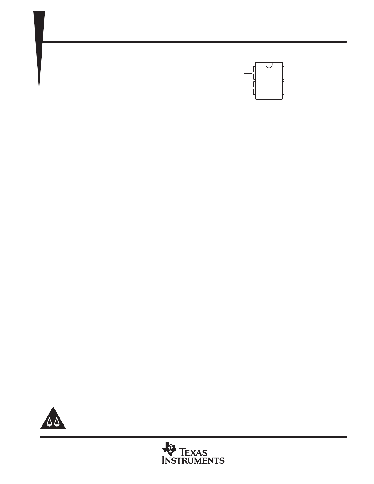
D OR P PACKAGE
(TOP VIEW)
SN75176A
DIFFERENTIAL BUS TRANSCEIVER
SLLS100A – JUNE 1984 – REVISED MAY 1995
2
POST OFFICE BOX 655303
•
DALLAS, TEXAS 75265
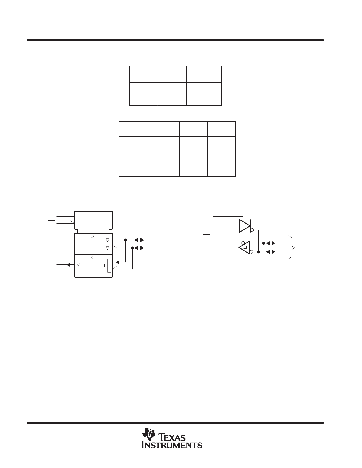
Function Tables
DRIVER
INPUT
ENABLE
OUTPUTS
D
DE
A
B
H
H
H
L
L
H
L
H
X
L
Z
Z
RECEIVER
DIFFERENTIAL INPUTS
ENABLE
OUTPUT
A – B
RE
R
VID
≥
0.2 V
L
H
– 0.2 V < VID < 0.2 V
L
?
VID
≤
– 0.2 V
L
L
X
H
Z
Open
L
?
H = high level, L = low level, ? = indeterminate,
X = irrelevant, Z = high impedance (off)
logic symbol
†
RE
DE
1
1
2
B
A
7
6
EN2
EN1
R
D
1
4
2
3
† This symbol is in accordance with ANSI/IEEE Std 91-1984
and IEC Publication 617-12.
logic diagram (positive logic)
DE
RE
R
6
7
3
1
2
B
A
Bus
D
4
SN75176A
DIFFERENTIAL BUS TRANSCEIVER
SLLS100A – JUNE 1984 – REVISED MAY 1995
3
POST OFFICE BOX 655303
•
DALLAS, TEXAS 75265
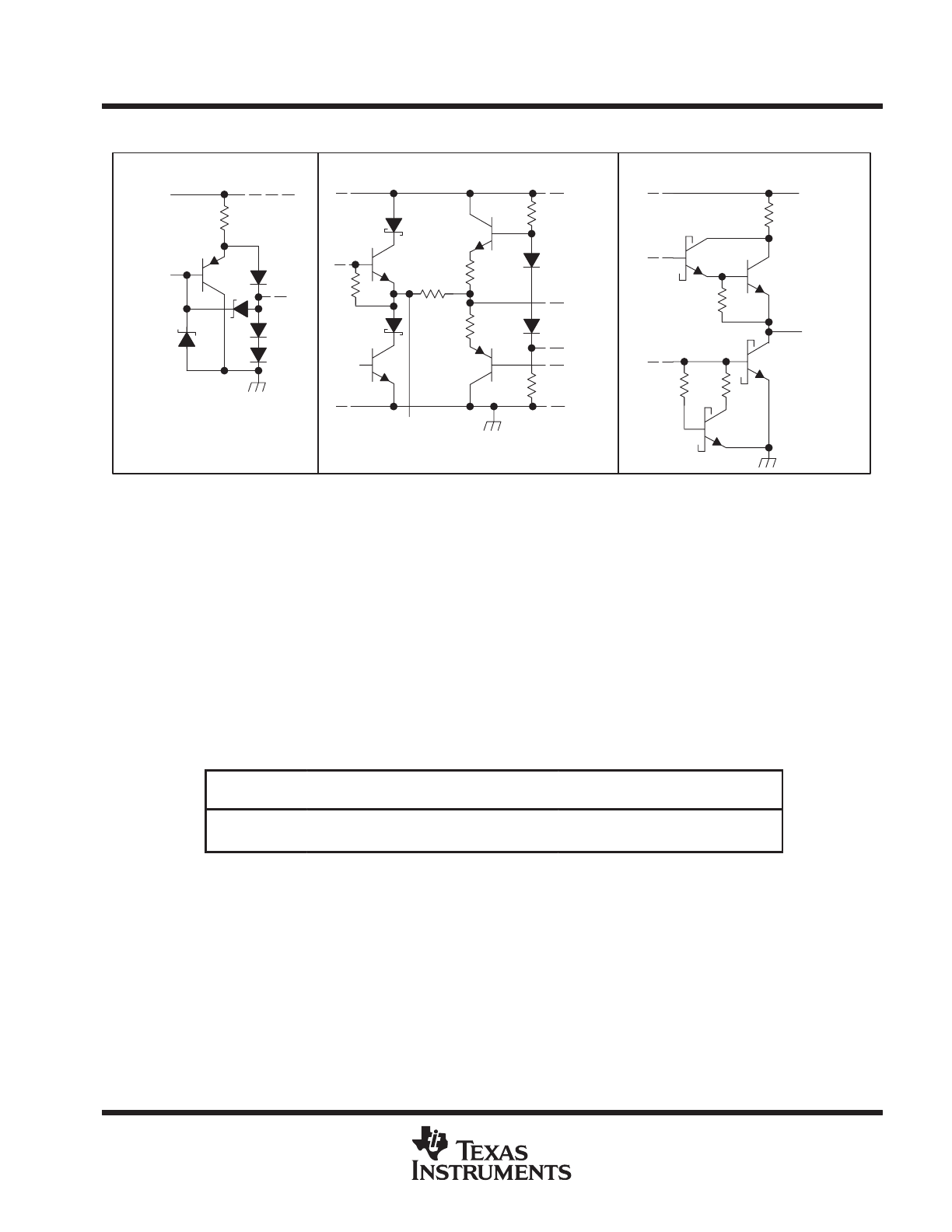
schematics of inputs and outputs
Output
85
Ω
NOM
TYPICAL OF RECEIVER OUTPUT
Input/Output
Port
960
Ω
NOM
16.8 k
Ω
NOM
TYPICAL OF A AND B I/O PORTS
Enable inputs: R(eq) = 8 k
Ω
NOM
Driver input: R(eq) = 3 k
Ω
NOM
R(eq)
VCC
EQUIVALENT OF EACH INPUT
VCC
Input
960
Ω
NOM
VCC
GND
R(eq) = equivalent resistor
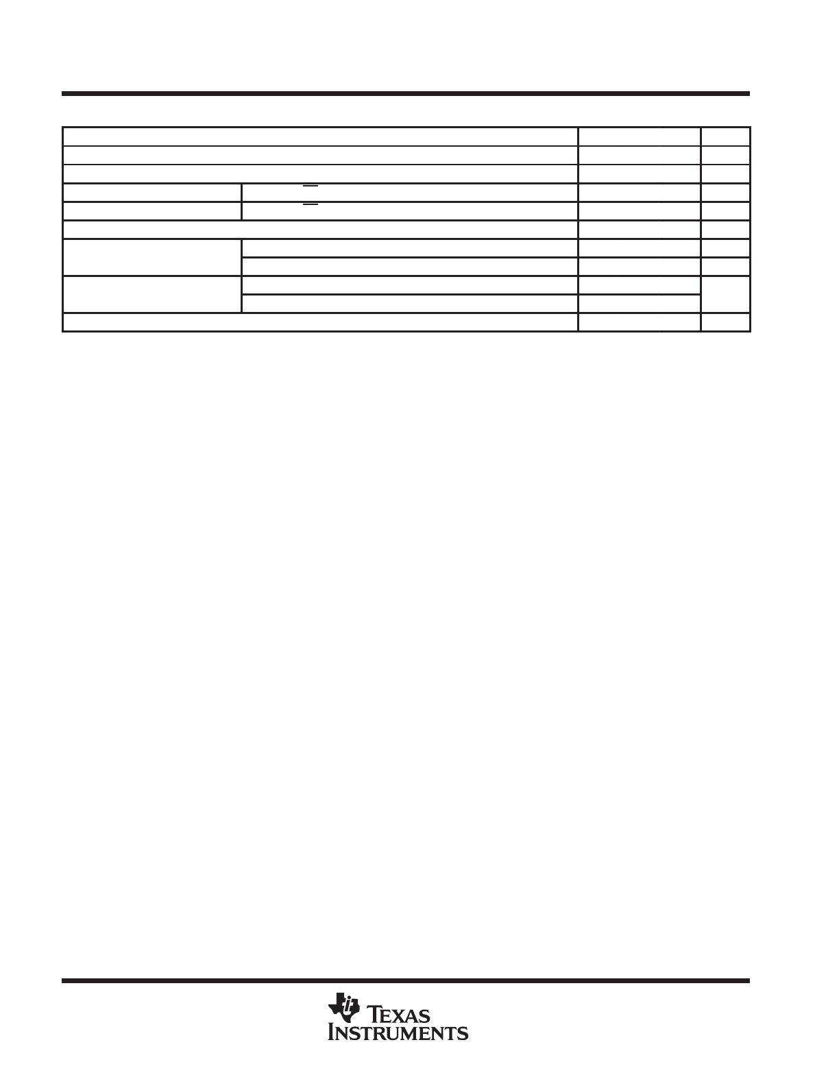
absolute maximum ratings over operating free-air temperature range (unless otherwise noted)
†
Supply voltage, V
CC
(see Note 1)
7 V
. . . . . . . . . . . . . . . . . . . . . . . . . . . . . . . . . . . . . . . . . . . . . . . . . . . . . . . . . . . . .
Voltage range at any bus terminal
– 10 V to 15 V
. . . . . . . . . . . . . . . . . . . . . . . . . . . . . . . . . . . . . . . . . . . . . . . . . . . .
Enable input voltage, V
I
5.5 V
. . . . . . . . . . . . . . . . . . . . . . . . . . . . . . . . . . . . . . . . . . . . . . . . . . . . . . . . . . . . . . . . . . . .
Continuous total power dissipation
See Dissipation Rating Table
. . . . . . . . . . . . . . . . . . . . . . . . . . . . . . . . . . . . .
Operating free-air temperature range, T
A
0
°
C to 70
°
C
. . . . . . . . . . . . . . . . . . . . . . . . . . . . . . . . . . . . . . . . . . . . . .
Storage temperature range, T
stg
– 65
°
C to 150
°
C
. . . . . . . . . . . . . . . . . . . . . . . . . . . . . . . . . . . . . . . . . . . . . . . . . . .
Lead temperature 1,6 mm (1/16 inch) from case for 10 seconds
260
°
C
. . . . . . . . . . . . . . . . . . . . . . . . . . . . . . .
† Stresses beyond those listed under “absolute maximum ratings” may cause permanent damage to the device. These are stress ratings only, and
functional operation of the device at these or any other conditions beyond those indicated under “recommended operating conditions” is not
implied. Exposure to absolute-maximum-rated conditions for extended periods may affect device reliability.
NOTE 1: All voltage values, except differential input/output bus voltage, are with respect to network ground terminal.
DISSIPATION RATING TABLE
PACKAGE
TA
≤
25
°
C
DERATING FACTOR
TA = 70
_
C
TA = 105
_
C
PACKAGE
A
POWER RATING
ABOVE TA = 25
°
C
A
POWER RATING
A
POWER RATING
D
725 mW
5.8 mW/
°
C
464 mW
261 mW
P
1100 mW
8.8 mW/
°
C
704 mW
396 mW
SN75176A
DIFFERENTIAL BUS TRANSCEIVER
SLLS100A – JUNE 1984 – REVISED MAY 1995
4
POST OFFICE BOX 655303
•
DALLAS, TEXAS 75265
recommended operating conditions
MIN
TYP
MAX
UNIT
Supply voltage, VCC
4.75
5
5.25
V
Voltage at any bus terminal (separately or common mode), VI or VIC
– 7
12
V
High-level input voltage, VIH
D, DE, and RE
2
V
Low-level input voltage, VIL
D, DE, and RE
0.8
V
Differential input voltage, VID (see Note 2)
±
12
V
High level output current IOH
Driver
– 60
mA
High-level output current, IOH
Receiver
– 400
µ
A
Low level output current IOL
Driver
60
mA
Low-level output current, IOL
Receiver
8
mA
Operating free-air temperature, TA
0
70
°
C
NOTE 2: Differential-input /output bus voltage is measured at the noninverting terminal A with respect to the inverting terminal B.
SN75176A
DIFFERENTIAL BUS TRANSCEIVER
SLLS100A – JUNE 1984 – REVISED MAY 1995
5
POST OFFICE BOX 655303
•
DALLAS, TEXAS 75265
DRIVER SECTION
electrical characteristics over recommended ranges of supply voltage and operating free-air
temperature (unless otherwise noted)
PARAMETER
TEST CONDITIONS
MIN
TYP†
MAX
UNIT
VIK
Input clamp voltage
II = – 18 mA
– 1.5
V
VOH
High level output voltage
VIH = 2 V,
VIL = 0.8 V,
3 7
V
VOH
High-level output voltage
IH
,
IOH = – 33 mA
IL
,
3.7
V
VOL
Low level output voltage
VIH = 2 V,
VIL = 0.8 V,
1 1
V
VOL
Low-level output voltage
IH
,
IOH = 33 mA
IL
,
1.1
V
|VOD1|
Differential output voltage
IO = 0
2VOD2
V
|VOD2|
Differential output voltage
RL = 100
Ω,
See Figure 1
2
2.7
V
|VOD2|
Differential output voltage
RL = 54
Ω,
See Figure 1
1.5
2.4
V
∆
|VOD|
Change in magnitude of differential output voltage ‡
±
0.2
V
VOC
Common-mode output voltage§
RL = 54
Ω
or 100
Ω,
See Figure 1
3
V
∆
|VOC|
Change in magnitude of common-mode output
±
0 2
V
∆
|VOC|
g
g
voltage ‡
±
0.2
V
IO
Output current
Output disabled,
VO = 12 V
1
mA
IO
Output current
,
See Note 3
VO = – 7 V
– 0.8
mA
IIH
High-level input current
VI = 2.4 V
20
µ
A
IIL
Low-level input current
VI = 0.4 V
– 400
µ
A
VO = – 7 V
– 250
IOS
Short-circuit output current
VO = VCC
250
mA
VO = 12 V
500
ICC
Supply current (total package)
No load
Outputs enabled
35
50
mA
ICC
Supply current (total package)
No load
Outputs disabled
26
40
mA
† All typical values are at VCC = 5 V and TA = 25
°
C.
‡
∆
|VOD| and
∆
|VOC| are the changes in magnitude of VOD and VOC respectively, that occur when the input is changed from a high level to a low
level.
§ In ANSI Standard EIA/TIA-422-B, VOC, which is the average of the two output voltages with respect to GND, is called output offset voltage, VOS.
NOTE 3: This applies for both power on and off; refer to ANSI Standard EIA/TIA-422-B for exact conditions.
switching characteristics, V
CC
= 5 V, T
A
= 25
°
C
PARAMETER
TEST CONDITIONS
MIN
TYP
MAX
UNIT
td(OD)
Differential-output delay time
RL = 60
Ω
See Figure 3
40
60
ns
tt(OD)
Differential-output transition time
RL = 60
Ω
,
See Figure 3
65
95
ns
tPZH
Output enable time to high level
RL = 110
Ω,
See Figure 4
55
90
ns
tPZL
Output enable time to low level
RL = 110
Ω,
See Figure 5
30
50
ns
tPHZ
Output disable time from high level
RL = 110
Ω,
See Figure 4
85
130
ns
tPLZ
Output disable time from low level
RL = 110
Ω,
See Figure 5
20
40
ns
SN75176A
DIFFERENTIAL BUS TRANSCEIVER
SLLS100A – JUNE 1984 – REVISED MAY 1995
6
POST OFFICE BOX 655303
•
DALLAS, TEXAS 75265
RECEIVER SECTION
electrical characteristics over recommended ranges of common-mode input voltage, supply
voltage, and operating free-air temperature (unless otherwise noted)
PARAMETER
TEST CONDITIONS
MIN
TYP†
MAX
UNIT
VIT +
Positive-going input threshold voltage
VO = 2.7 V,
IO = – 0.4 mA
0.2
V
VIT–
Negative-going input threshold voltage
VO = 0.5 V,
IO = 8 mA
– 0.2‡
V
Vhys
Input hysteresis voltage (VIT + – VIT –)
50
mV
VIK
Enable clamp voltage
II = – 18 mA
– 1.5
V
VOH
High level output voltage
VID = 200 mV,
IOH = – 400
µ
A,
2 7
V
VOH
High-level output voltage
ID
,
See Figure 2
OH
µ
,
2.7
V
VOL
Low level output voltage
VID = – 200 mV,
IOL = 8 mA,
0 45
V
VOL
Low-level output voltage
ID
,
See Figure 2
OL
,
0.45
V
IOZ
High-impedance-state output current
VO = 0.4 V to 2.4 V
±
20
µ
A
II
Line input current
Other input = 0 V,
VI = 12 V
1
mA
II
Line input current
,
See Note 3
VI = – 7 V
– 0.8
mA
IIH
High-level enable input current
VIH = 2.7 V
20
µ
A
IIL
Low-level enable input current
VIL = 0.4 V
– 100
µ
A
ri
Input resistance
12
k
Ω
IOS
Short-circuit output current
– 15
– 85
mA
ICC
Supply current (total package)
No load
Outputs enabled
35
50
mA
ICC
Supply current (total package)
No load
Outputs disabled
26
40
mA
† All typical values are at VCC = 5 V, TA = 25
°
C.
‡ The algebraic convention, in which the less-positive (more-negative) limit is designated minimum, is used in this data sheet for common-mode
input voltage and threshold voltage levels only.
NOTE 3: This applies for both power on and power off. Refer to ANSI Standard EIA/TIA-422-B for exact conditions.
switching characteristics, V
CC
= 5 V, C
L
= 15 pF, T
A
= 25
°
C
PARAMETER
TEST CONDITIONS
MIN
TYP
MAX
UNIT
tPLH
Propagation delay time, low-to-high-level output
VID = 1 5 V to 1 5 V
See Figure 6
21
35
ns
tPHL
Propagation delay time, high-to-low-level output
VID = – 1.5 V to 1.5 V, See Figure 6
23
35
ns
tPZH
Output enable time to high level
See Figure 7
10
30
ns
tPZL
Output enable time to low level
See Figure 7
12
30
ns
tPHZ
Output disable time from high level
See Figure 7
20
35
ns
tPLZ
Output disable time from low level
See Figure 7
17
25
ns
SN75176A
DIFFERENTIAL BUS TRANSCEIVER
SLLS100A – JUNE 1984 – REVISED MAY 1995
7
POST OFFICE BOX 655303
•
DALLAS, TEXAS 75265
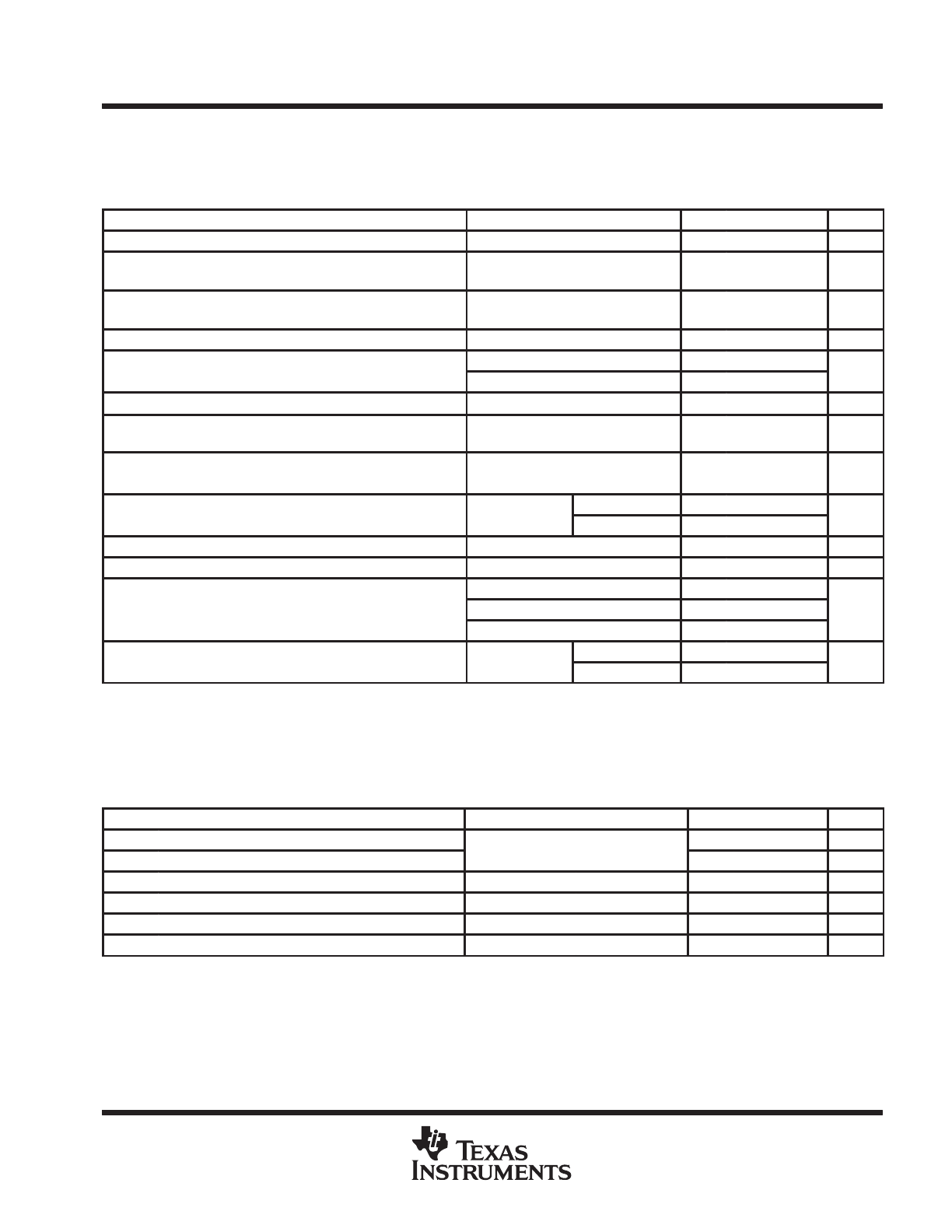
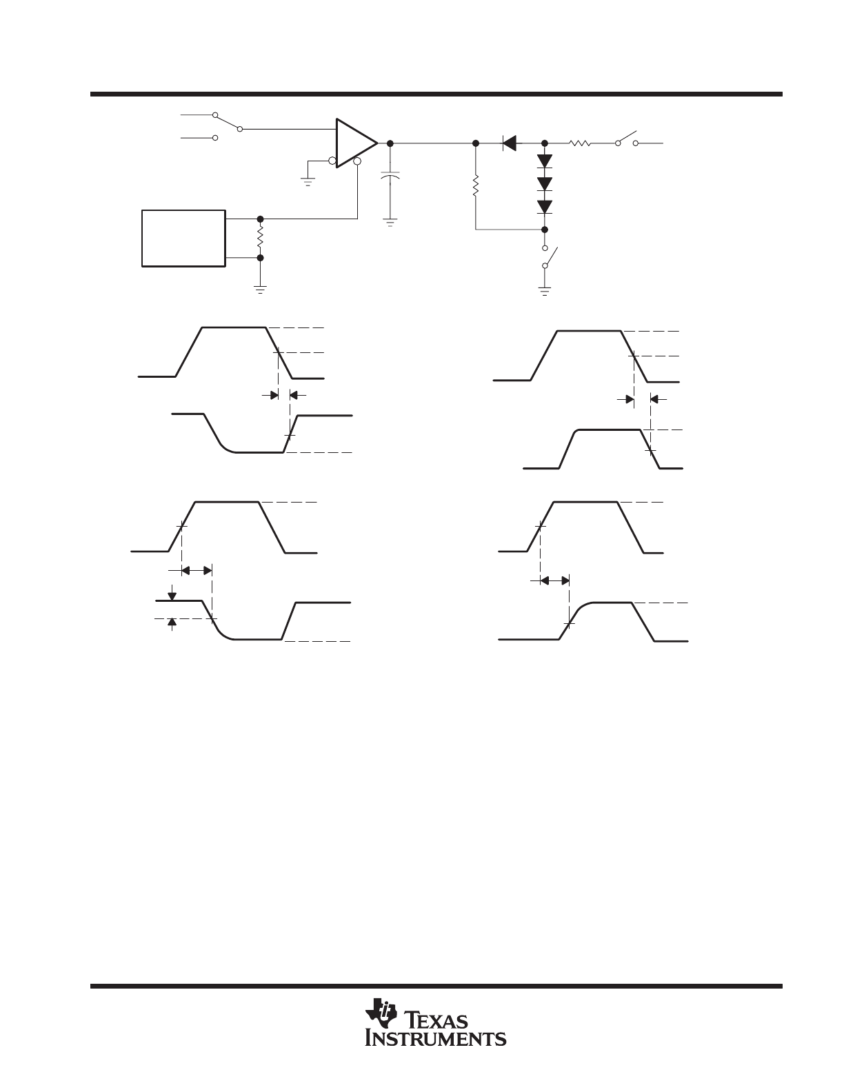
PARAMETER MEASUREMENT INFORMATION
2
RL
VOD2
VOC
2
RL
Figure 1. Driver V
OD
and V
OC
VOL
VOH
– IOH
+IOL
VID
0 V
Figure 2. Receiver V
OH
and V
OL
3 V
VOLTAGE WAVEFORMS
tt(OD)
td(OD)
1.5 V
10%
tt(OD)
≈
2.5 V
≈
– 2.5 V
90%
50%
Output
td(OD)
0 V
3 V
1.5 V
Input
TEST CIRCUIT
Output
CL = 50 pF
(see Note B)
50
Ω
RL = 60
Ω
Generator
(see Note A)
50%
10%
CL
NOTES: A. The input pulse is supplied by a generator having the following characteristics: PRR = 1 MHz, 50% duty cycle, tr
≤
6 ns, tf
≤
6 ns,
ZO = 50
Ω
.
B. CL includes probe and jig capacitance.
Figure 3. Driver Test Circuit and Voltage Waveforms
VOLTAGE WAVEFORMS
tPHZ
1.5 V
2.3 V
0.5 V
0 V
3 V
tPZH
Output
Input
1.5 V
S1
0 or 3 V
Output
CL = 50 pF
(see Note B)
TEST CIRCUIT
50
Ω
VOH
Voff
≈
0 V
RL = 110
Ω
Generator
(see Note A)
NOTES: A. The input pulse is supplied by a generator having the following characteristics: PRR = 1 MHz, 50% duty cycle, tr
≤
6 ns, tf
≤
6 ns,
ZO = 50
Ω
.
B. CL includes probe and jig capacitance.
Figure 4. Driver Test Circuit and Voltage Waveforms
SN75176A
DIFFERENTIAL BUS TRANSCEIVER
SLLS100A – JUNE 1984 – REVISED MAY 1995
8
POST OFFICE BOX 655303
•
DALLAS, TEXAS 75265
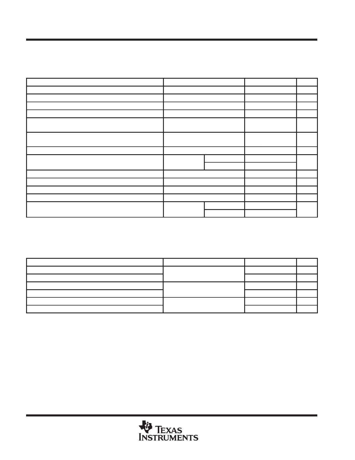
VOLTAGE WAVEFORMS
5 V
VOL
0.5 V
tPZL
3 V
0 V
tPLZ
2.3 V
1.5 V
Output
Input
TEST CIRCUIT
Output
RL = 110
Ω
5 V
S1
CL = 50 pF
(see Note B)
50
Ω
3 V or 0
Generator
(see Note A)
1.5 V
NOTES: A. The input pulse is supplied by a generator having the following characteristics: PRR = 1 MHz, 50% duty cycle, tr
≤
6 ns, tf
≤
6 ns,
ZO = 50
Ω
.
B. CL includes probe and jig capacitance.
Figure 5. Driver Test Circuit and Voltage Waveforms
VOLTAGE WAVEFORMS
1.3 V
0 V
3 V
VOL
VOH
tPHL
tPLH
1.5 V
Output
Input
TEST CIRCUIT
CL = 15 pF
(see Note B)
Output
0 V
1.5 V
51
Ω
Generator
(see Note A)
1.5 V
1.3 V
NOTES: A. The input pulse is supplied by a generator having the following characteristics: PRR = 1 MHz, 50% duty cycle, tr
≤
6 ns, tf
≤
6 ns,
ZO = 50
Ω
.
B. CL includes probe and jig capacitance.
Figure 6. Receiver Test Circuit and Voltage Waveforms
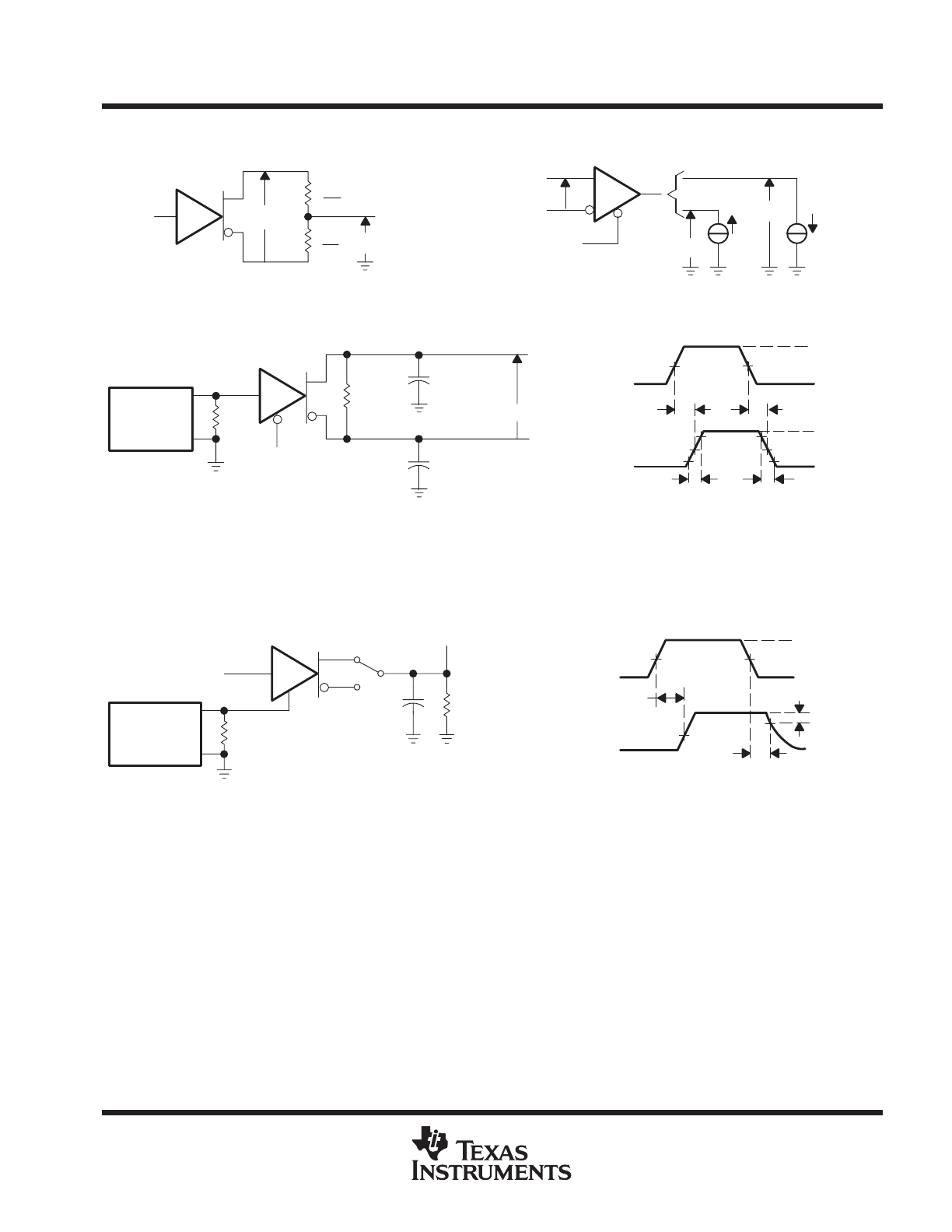
SN75176A
DIFFERENTIAL BUS TRANSCEIVER
SLLS100A – JUNE 1984 – REVISED MAY 1995
9
POST OFFICE BOX 655303
•
DALLAS, TEXAS 75265
VOH
0.5 V
≈
1.3 V
tPHZ
Output
Input
1.5 V
0 V
3 V
S1 to 1.5 V
S2 Closed
S3 Closed
tPLZ
≈
1.3 V
VOL
0.5 V
Output
Input
1.5 V
0 V
3 V
≈
4.5 V
VOL
1.5 V
S3 Open
S2 Closed
S1 to –1.5 V
0 V
1.5 V
3 V
tPZL
Output
Input
0 V
1.5 V
VOH
0 V
Output
Input
tPZH
S3 Closed
S2 Open
S1 to 1.5 V
1.5 V
3 V
TEST CIRCUIT
50
Ω
1N916 or Equivalent
S3
5 V
S2
2 k
Ω
5 k
Ω
S1
–1.5 V
1.5 V
VOLTAGE WAVEFORMS
S1 to – 1.5 V
S2 Closed
S3 Closed
Generator
(see Note A)
CL = 15 pF
(see Note B)
NOTES: A. The input pulse is supplied by a generator having the following characteristics: PRR = 1 MHz, 50% duty cycle, tr
≤
6 ns, tf
≤
6 ns,
ZO = 50
Ω
.
B. CL includes probe and jig capacitance.
Figure 7. Receiver Test Circuit and Voltage Waveforms
SN75176A
DIFFERENTIAL BUS TRANSCEIVER
SLLS100A – JUNE 1984 – REVISED MAY 1995
10
POST OFFICE BOX 655303
•
DALLAS, TEXAS 75265
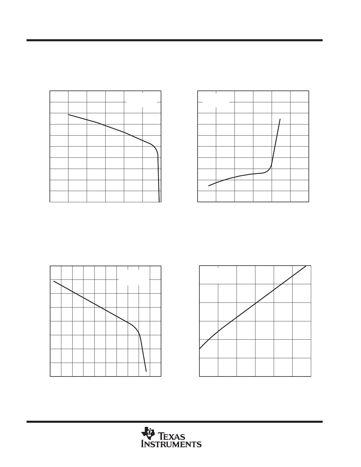
TYPICAL CHARACTERISTICS
Figure 8
VOH – High-Level Output V
oltage – V
DRIVER
HIGH-LEVEL OUTPUT VOLTAGE
vs
HIGH-LEVEL OUTPUT CURRENT
VCC = 5 V
4.5
4
3.5
3
2.5
2
1.5
1
0.5
– 100
– 80
– 60
– 40
– 20
0
– 120
5
IOH – High-Level Output Current – mA
0
V
OH
TA = 25
°
C
Figure 9
DRIVER
LOW-LEVEL OUTPUT VOLTAGE
vs
LOW-LEVEL OUTPUT CURRENT
VCC = 5 V
TA = 25
°
C
IOL – Low-Level Output Current – mA
0
120
20
40
60
80
100
5
0
0.5
1
1.5
2
2.5
3
3.5
4
4.5
– Low-Level Output V
oltage – V
V
OL
Figure 10
VOD – Differential Output V
oltage – V
DRIVER
DIFFERENTIAL OUTPUT VOLTAGE
vs
OUTPUT CURRENT
3.5
3
2.5
2
1.5
1
0.5
90
80
70
60
50
40
30
20
10
0
100
4
IO – Output Current – mA
0
V
OD
VCC = 5 V
TA = 25
°
C
Figure 11
VCC = 5 V
TA = 25
°
C
0.3
0.2
0.1
0
0
5
10
VOL
– Low-Level Output V
oltage – V
0.4
0.5
RECEIVER
LOW-LEVEL OUTPUT VOLTAGE
vs
LOW-LEVEL OUTPUT CURRENT
0.6
15
20
25
30
IOL – Low Level Output Current – mA
ÁÁ
ÁÁ
ÁÁ
V
OL
SN75176A
DIFFERENTIAL BUS TRANSCEIVER
SLLS100A – JUNE 1984 – REVISED MAY 1995
11
POST OFFICE BOX 655303
•
DALLAS, TEXAS 75265
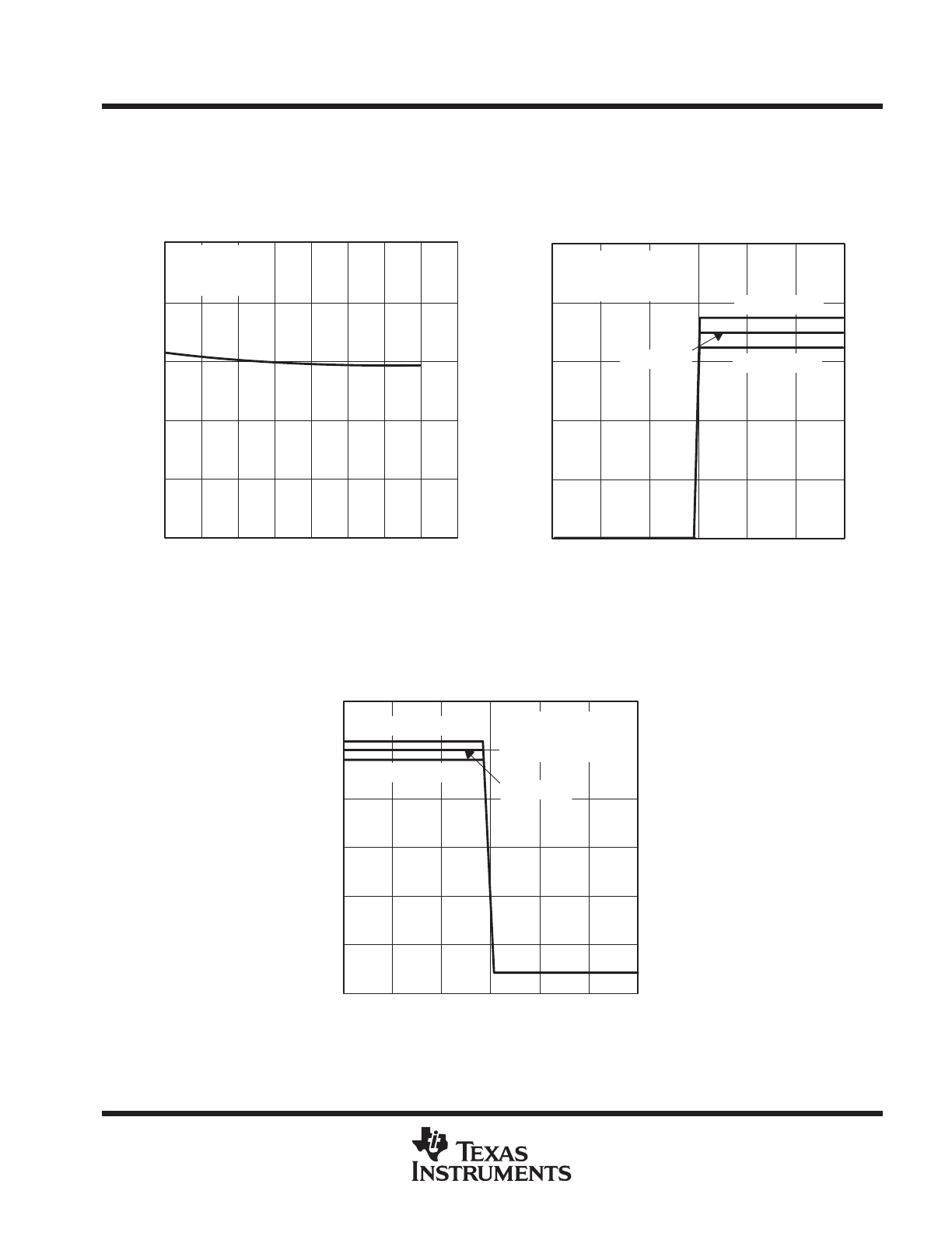
TYPICAL CHARACTERISTICS
Figure 12
RECEIVER
LOW-LEVEL OUTPUT VOLTAGE
vs
FREE-AIR TEMPERATURE
0.3
0.2
0.1
0
0
20
30
50
VOL
– Low-Levcel Output V
oltage – V
0.4
0.5
70
80
10
40
60
VCC = 5 V
VID = – 0.2 V
IOL = 8 mA
ÁÁ
ÁÁ
ÁÁ
V
OL
TA – Free-Air Temperature –
°
C
Figure 13
2
1
0
0
0.5
1
1.5
VO – Output V
oltage – V
3
4
RECEIVER
OUTPUT VOLTAGE
vs
ENABLE VOLTAGE
5
2
2.5
3
VID = 0.2 V
Load = 8 k
Ω
to GND
TA = 25
°
C
VCC = 5 V
VCC = 4.75 V
ÁÁ
ÁÁ
V
O
VI – Enable Voltage – V
VCC = 5.25 V
3
2
1
0
0
0.5
1
VO – Output V
oltage – V
4
5
RECEIVER
OUTPUT VOLTAGE
vs
ENABLE VOLTAGE
6
1.5
2
2.5
3
VID = 0.2 V
Load = 1 k
Ω
to VCC
TA = 25
°
C
VCC = 5.25 V
VCC = 5 V
VCC = 4.75 V
ÁÁ
ÁÁ
V
O
VI – Enable Voltage – V
Figure 14
SN75176A
DIFFERENTIAL BUS TRANSCEIVER
SLLS100A – JUNE 1984 – REVISED MAY 1995
12
POST OFFICE BOX 655303
•
DALLAS, TEXAS 75265
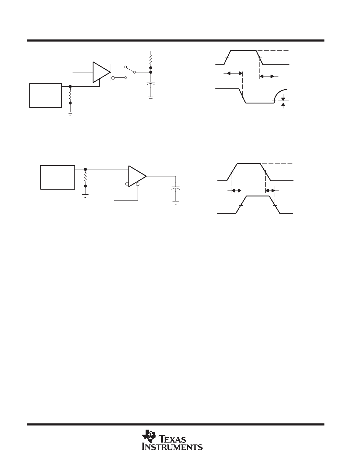
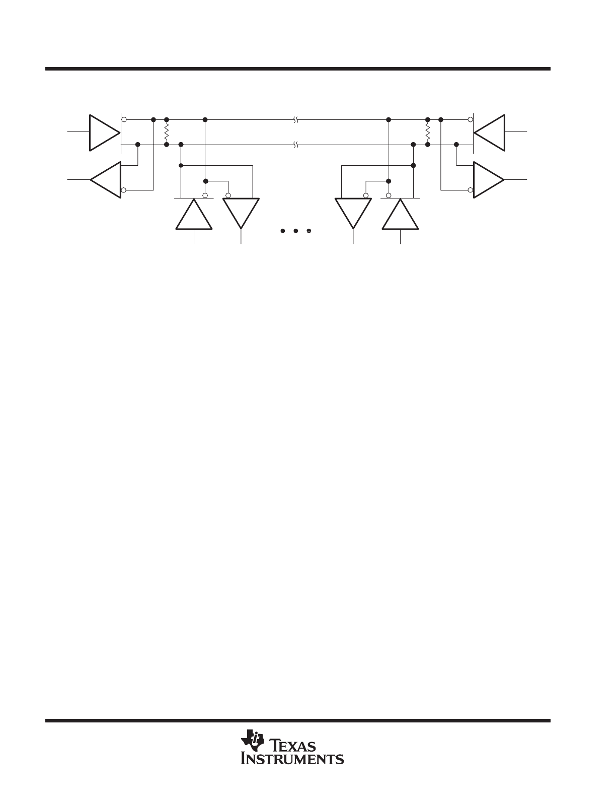
APPLICATION INFORMATION
Up to 32
Transceivers
SN65176A
SN65176A
RT
RT
NOTE A: The line should be terminated at both ends in its characteristic impedance (RT = ZO). Stub lengths off the main line should be kept
as short as possible.
Figure 15. Typical Application Circuit

IMPORTANT NOTICE
Texas Instruments and its subsidiaries (TI) reserve the right to make changes to their products or to discontinue
any product or service without notice, and advise customers to obtain the latest version of relevant information
to verify, before placing orders, that information being relied on is current and complete. All products are sold
subject to the terms and conditions of sale supplied at the time of order acknowledgement, including those
pertaining to warranty, patent infringement, and limitation of liability.
TI warrants performance of its semiconductor products to the specifications applicable at the time of sale in
accordance with TI’s standard warranty. Testing and other quality control techniques are utilized to the extent
TI deems necessary to support this warranty. Specific testing of all parameters of each device is not necessarily
performed, except those mandated by government requirements.
CERTAIN APPLICATIONS USING SEMICONDUCTOR PRODUCTS MAY INVOLVE POTENTIAL RISKS OF
DEATH, PERSONAL INJURY, OR SEVERE PROPERTY OR ENVIRONMENTAL DAMAGE (“CRITICAL
APPLICATIONS”). TI SEMICONDUCTOR PRODUCTS ARE NOT DESIGNED, AUTHORIZED, OR
WARRANTED TO BE SUITABLE FOR USE IN LIFE-SUPPORT DEVICES OR SYSTEMS OR OTHER
CRITICAL APPLICATIONS. INCLUSION OF TI PRODUCTS IN SUCH APPLICATIONS IS UNDERSTOOD TO
BE FULLY AT THE CUSTOMER’S RISK.
In order to minimize risks associated with the customer’s applications, adequate design and operating
safeguards must be provided by the customer to minimize inherent or procedural hazards.
TI assumes no liability for applications assistance or customer product design. TI does not warrant or represent
that any license, either express or implied, is granted under any patent right, copyright, mask work right, or other
intellectual property right of TI covering or relating to any combination, machine, or process in which such
semiconductor products or services might be or are used. TI’s publication of information regarding any third
party’s products or services does not constitute TI’s approval, warranty or endorsement thereof.
Copyright
1998, Texas Instruments Incorporated