
TIP110/112
TIP115/117
COMPLEMENTARY SILICON POWER
DARLINGTON TRANSISTORS
■
STMicroelectronics PREFERRED
SALESTYPES
■
COMPLEMENTARY PNP - NPN DEVICES
■
MONOLITHIC DARLINGTON
CONFIGURATION
■
INTEGRATED ANTIPARALLEL
COLLECTOR-EMITTER DIODE
APPLICATIONS
■
LINEAR AND SWITCHING INDUSTRIAL
EQUIPMENT
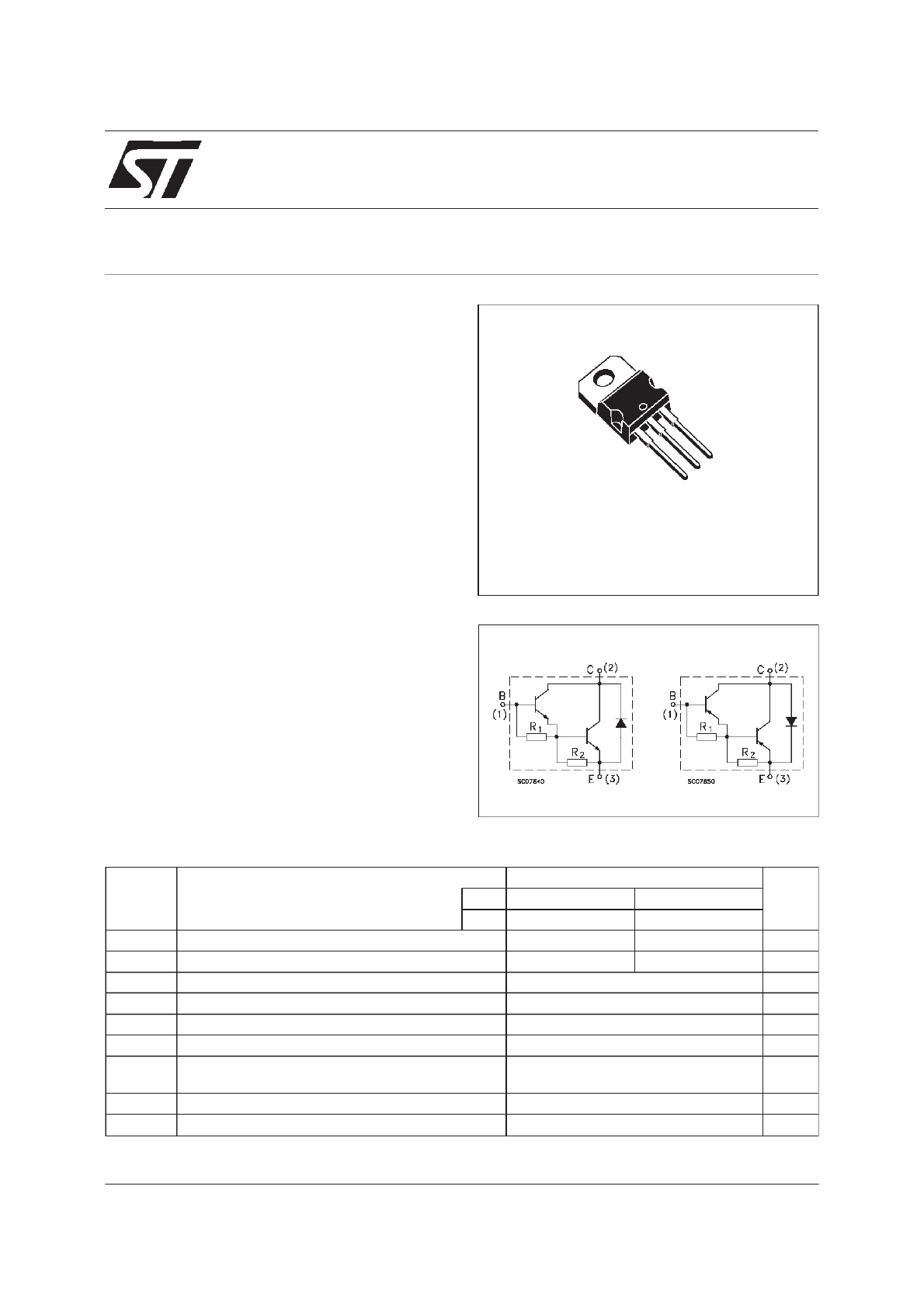
DESCRIPTION
The
TIP110
and
TIP112
are
silicon
Epitaxial-Base NPN transistors in monolithic
Darlington
configuration
mounted
in
Jedec
TO-220 plastic package. They are intented for
use in medium power linear and switching
applications.
The complementary PNP types are TIP115 and
TIP117.
INTERNAL SCHEMATIC DIAGRAM
R
1
T yp. = 7K
Ω
R
2
T yp.= 230
June 1999
1
2
3
TO-220
ABSOLUTE MAXIMUM RATINGS
Symbol
Parameter
Val ue
Uni t
NPN
TIP110
TIP112
PNP
TIP115
TIP117
V
CBO
Collect or-Base Voltage (I
E
= 0)
60
100
V
V
CEO
Collect or-Emitter Voltage (I
B
= 0)
60
100
V
V
EBO
Emitter-Base Voltage (I
C
= 0)
5
V
I
C
Collect or Current
2
A
I
CM
Collect or Peak Current
4
A
I
B
Base Current
50
mA
P
t ot
Tot al Dissipation at T
cas e
≤
25
o
C
T
am b
≤
25
o
C
50
2
W
W
T
stg
Storage T emperat ure
-65 to 150
o
C
T
j
Max. O perating Junction Temperature
150
o
C
* For PNP types voltage and current values are negative
1/6
THERMAL DATA
R
t hj-ca se
R
t hj- amb
Thermal Resistance Junction-case
Max
Thermal Resistance Junction-ambient
Max
2.5
62.5
o
C/W
o
C/W
ELECTRICAL CHARACTERISTICS (T
case
= 25
o
C unless otherwise specified)
Symb ol
Parameter
Test Cond ition s
Mi n.
Typ .
Max.
Un it
I
CEO
Collector Cut -of f
Current (I
B
= 0)
V
CE
= Half Rated V
CEO
2
mA
I
CBO
Collector Cut -of f
Current (I
E
= 0)
V
CB
= Rated V
CBO
1
mA
I
EBO
Emitt er Cut -of f Current
(I
C
= 0)
V
EB
= 5 V
2
mA
V
CEO(sus )
∗
Collector-Emit ter
Sustaining Voltage
(I
B
= 0)
I
C
= 30 mA
for TIP110/115
for TIP112/117
60
100
V
V
V
CE(sat )
∗
Collector-Emit ter
Saturation Voltage
I
C
= 2 A
I
B
= 8 mA
2.5
V
V
BE
∗
Base-Emitt er Voltage
I
C
= 2 A
V
CE
= 4 V
2.8
V
h
F E
∗
DC Current Gain
I
C
= 1 A
V
CE
= 4 V
I
C
= 2 A
V
CE
= 4 V
1000
500
∗
Pulsed: Pulse duration = 300
µ
s, duty cycle 1.5 %
For PNP types voltage and current values are negative.
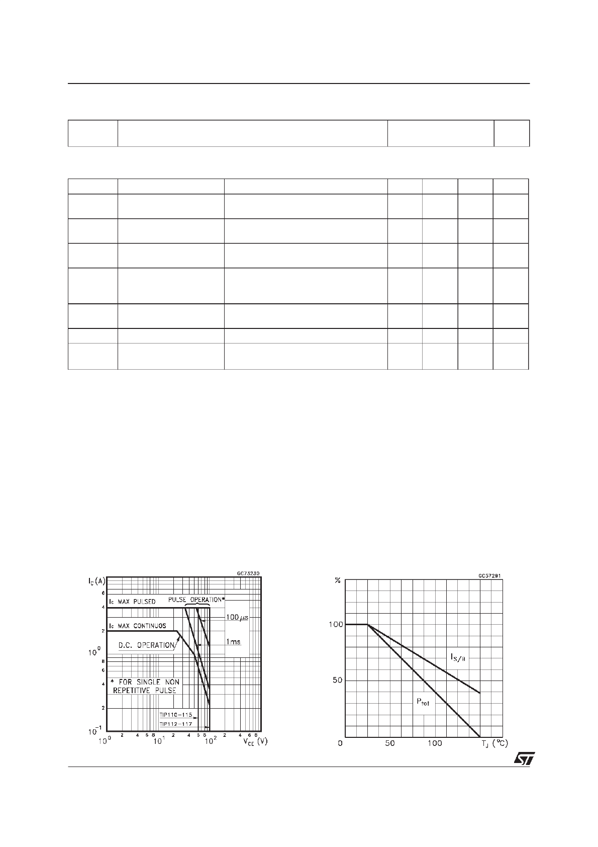
Safe Operating Areas
Derating Curve
TIP110/TIP112/TIP115/TIP117
2/6
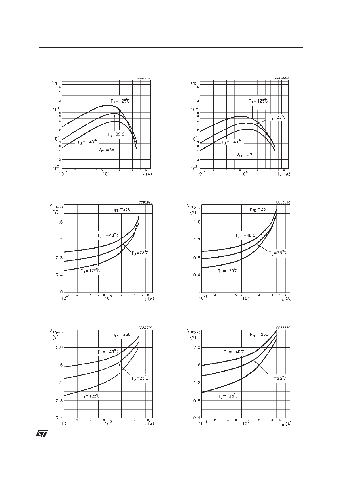
DC Current Gain (NPN type)
Collector-Emitter Saturation Voltage (NPN type)
Base-Emitter Saturation Voltage (NPN type)
DC Current Gain (PNP type)
Collector-Emitter Saturation Voltage (PNP type)
Base-Emitter Saturation Voltage (PNP type)
TIP110/TIP112/TIP115/TIP117
3/6
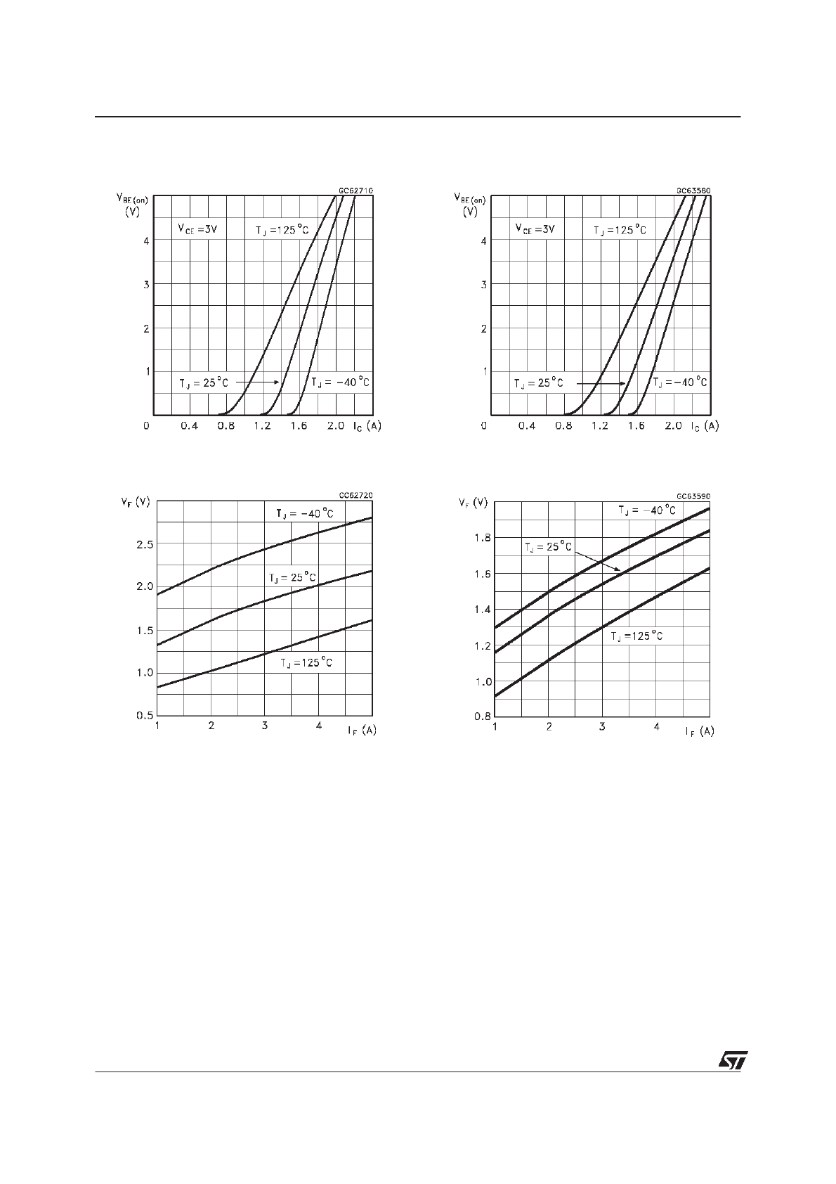
Base-Emitter On Voltage (NPN type)
Base-Emitter On Voltage (PNP type)
Freewheel Diode Forward Voltage (NPN types)
Freewheel Diode Forward Voltage (PNP types)
TIP110/TIP112/TIP115/TIP117
4/6
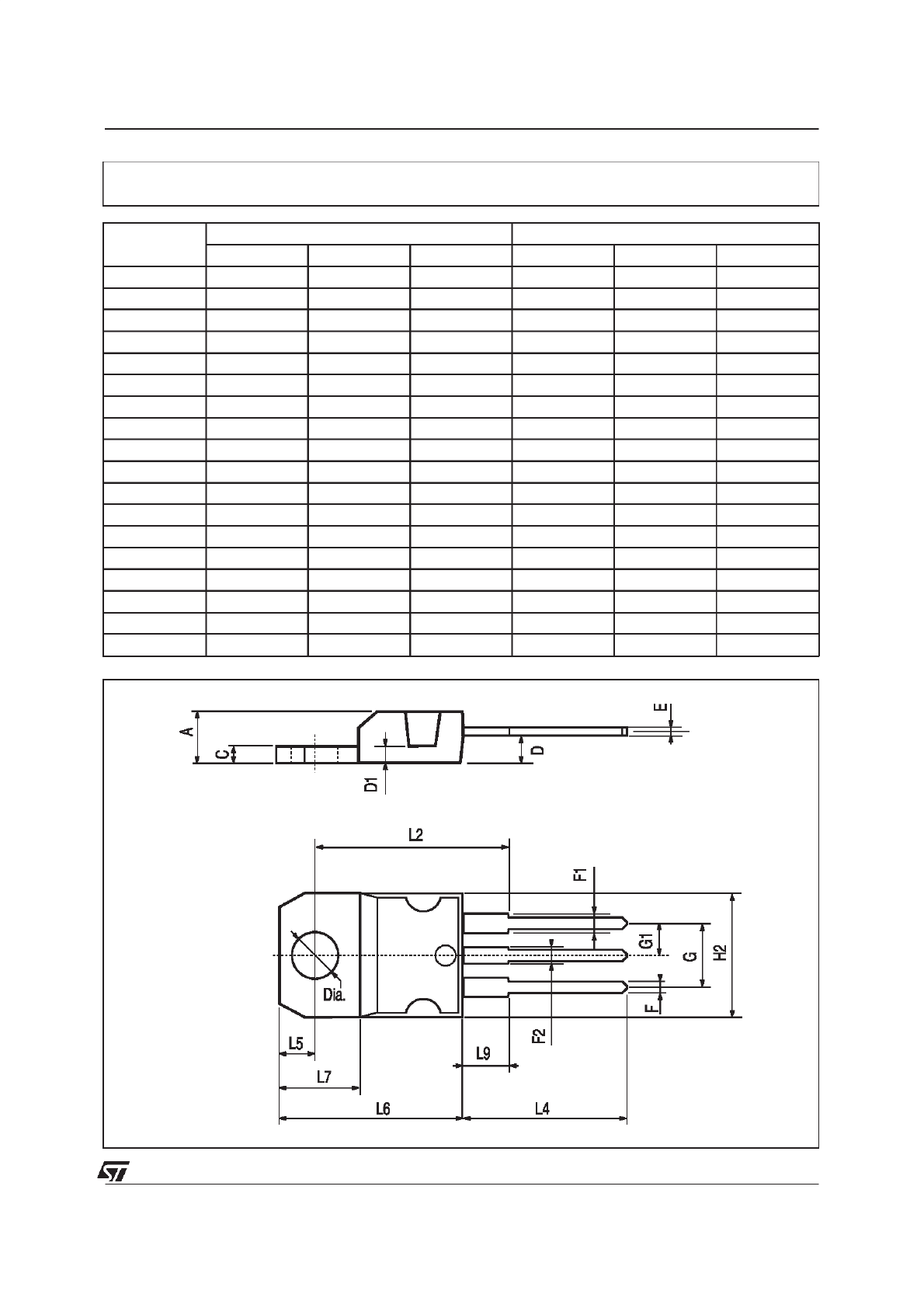
DIM.
mm
inch
MIN.
TYP.
MAX.
MIN.
TYP.
MAX.
A
4.40
4.60
0.173
0.181
C
1.23
1.32
0.048
0.051
D
2.40
2.72
0.094
0.107
D1
1.27
0.050
E
0.49
0.70
0.019
0.027
F
0.61
0.88
0.024
0.034
F1
1.14
1.70
0.044
0.067
F2
1.14
1.70
0.044
0.067
G
4.95
5.15
0.194
0.203
G1
2.4
2.7
0.094
0.106
H2
10.0
10.40
0.393
0.409
L2
16.4
0.645
L4
13.0
14.0
0.511
0.551
L5
2.65
2.95
0.104
0.116
L6
15.25
15.75
0.600
0.620
L7
6.2
6.6
0.244
0.260
L9
3.5
3.93
0.137
0.154
DIA.
3.75
3.85
0.147
0.151
P011C
TO-220 MECHANICAL DATA
TIP110/TIP112/TIP115/TIP117
5/6

Information furnished is believed to be accurate and reliable. However, STMicroelectronics assumes no responsibility for the consequences
of use of such information nor for any infringement of patents or other rights of third parties which may result from its use. No license is
granted by implication or otherwise under any patent or patent rights of STMicroelectronics. Specification mentioned in this publication are
subject to change without notice. This publication supersedes and replaces all information previously supplied. STMicroelectronics products
are not authorized for use as critical components in life support devices or systems without express written approval of STMicroelectronics.
The ST logo is a trademark of STMicroelectronics
1999 STMicroelectronics – Printed in Italy – All Rights Reserved
STMicroelectronics GROUP OF COMPANIES
Australia - Brazil - Canada - China - France - Germany - Italy - Japan - Korea - Malaysia - Malta - Mexico - Morocco - The Netherlands -
Singapore - Spain - Sweden - Switzerland - Taiwan - Thailand - United Kingdom - U.S.A.
http://www.st.com
.
TIP110/TIP112/TIP115/TIP117
6/6