
1/9
■
LOW POWER CONSUMPTION
■
WIDE COMMON-MODE (UP TO V
CC
+
) AND
DIFFERENTIAL VOLTAGE RANGE
■
LOW INPUT BIAS AND OFFSET CURRENT
■
OUTPUT SHORT-CIRCUIT PROTECTION
■
HIGH INPUT IMPEDANCE J–FET INPUT
STAGE
■
INTERNAL FREQUENCY COMPENSATION
■
LATCH UP FREE OPERATION
■
HIGH SLEW RATE : 16V/
µ
s (typ)
DESCRIPTION
The LF353 are high speed J–FET input dual oper-
ational amplifiers incorporating well matched, high
voltage J–FET and bipolar transistors in a mono-
lithic integrated circuit.
The devices feature high slew rates, low input bias
and offset currents, and low offset voltage temper-
ature coefficient.
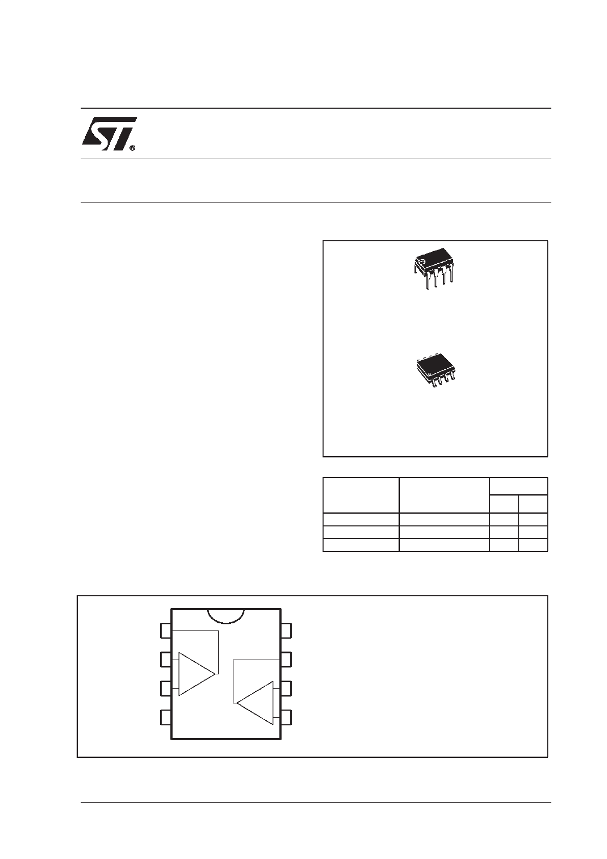
ORDER CODE
N = Dual in Line Package (DIP)
D = Small Outline Package (SO) - also available in Tape & Reel (DT)
PIN CONNECTIONS (top view)
Part Number
Temperature Range
Package
N
D
LF353
0
°
C, +70
°
C
•
•
LF253
-40
°
C, +105
°
C
•
•
LF153
-55
°
C, +125
°
C
•
•
N
DIP8
(Plastic Package)
D
SO8
(Plastic Micropackage)
1
2
3
4
5
6
7
8
-
+
-
+
1 - Output1
2 - Inverting input 1
3 - Non-inverting input 1
4 - V
CC
-
5 - Non-invertig input 2
6 - Inverting input 2
7 - Output 2
8 - V
CC
+
LF153
LF253 - LF353
WIDE BANDWIDTH
DUAL J-FET OPERATIONAL AMPLIFIERS
March 2001
LF153 - LF253 - LF353
2/9
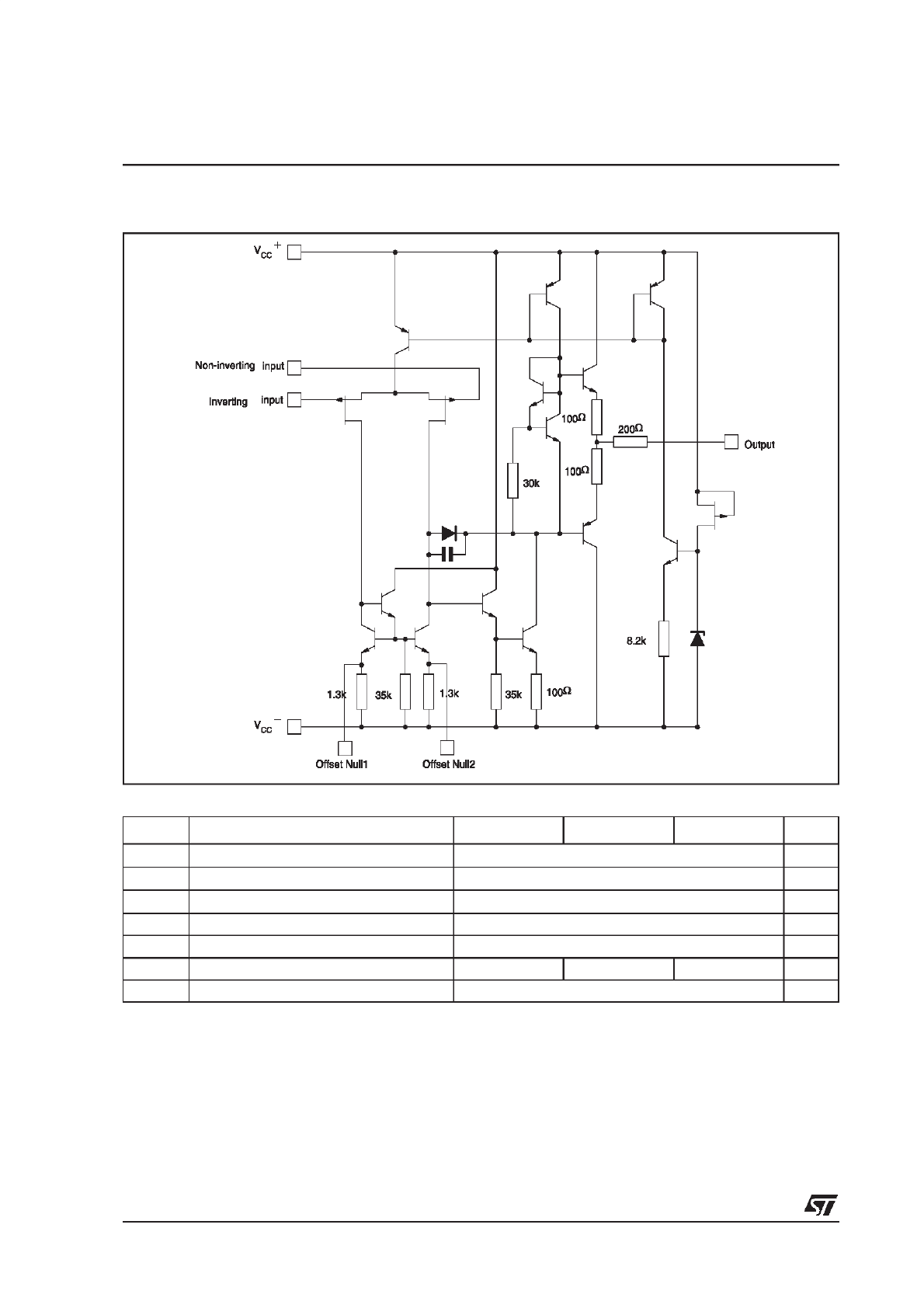
SCHEMATIC DIAGRAM (each amplifier)
ABSOLUTE MAXIMUM RATINGS
Symbol
Parameter
LF153
LF253
LF353
Unit
V
CC
Supply voltage - note
1)
1.
All voltage values, except differential voltage, are with respect to the zero reference level (ground) of the supply voltages where the zero reference
level is the midpoint between V
CC
+
and V
CC
-
.
±
18
V
V
i
Input Voltage - note
2)
2.
The magnitude of the input voltage must never exceed the magnitude of the supply voltage or 15 volts, whichever is less.
±
15
V
V
id
Differential Input Voltage - note
3)
3.
Differential voltages are the non-inverting input terminal with respect to the inverting input terminal.
±
30
V
P
tot
Power Dissipation
680
mW
Output Short-circuit Duration - note
4)
4.
The output may be shorted to ground or to either supply. Temperature and/or supply voltages must be limited to ensure that the dissipation rating
is not exceeded
Infinite
T
oper
Operating Free-air Temperature Range
-55 to +125
-40 to +105
0 to +70
°
C
T
stg
Storage Temperature Range
-65 to +150
°
C
LF153 - LF253 - LF353
3/9
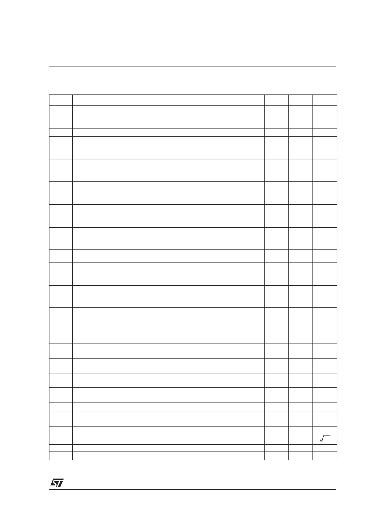
ELECTRICAL CHARACTERISTICS
V
CC
=
±
15V, T
amb
= +25
°
C (unless otherwise specified)
Symbol
Parameter
Min.
Typ.
Max.
Unit
V
io
Input Offset Voltage (R
s
=
10k
Ω
)
T
amb
= +25
°
C
T
min
≤
T
amb
≤
T
max
3
10
13
mV
DV
io
Input Offset Voltage Drift
10
µ
V/
°
C
I
io
Input Offset Current- note
1)
T
amb
= +25
°
C
T
min
≤
T
amb
≤
T
max
1.
The input bias currents are junction leakage currents which approximately double for every 10
°
C increase in the junction temperature.
5
100
4
pA
nA
I
ib
Input Bias Current -note 1
T
amb
= +25
°
C
T
min
≤
T
amb
≤
T
max
20
200
20
nA
A
vd
Large Signal Voltage Gain
(
R
L
= 2k
Ω
, V
o
=
±
10V)
T
amb
= +25
°
C
T
min
≤
T
amb
≤
T
max
50
25
200
V/mV
SVR
Supply Voltage Rejection Ratio (R
S
=
10k
Ω)
T
amb
= +25
°
C
T
min
≤
T
amb
≤
T
max
80
80
86
dB
I
CC
Supply Current, no load
T
amb
= +25
°
C
T
min
≤
T
amb
≤
T
max
1.4
3.2
3.2
mA
V
icm
Input Common Mode Voltage Range
±
11
+15
-12
V
CMR
Common Mode Rejection Ratio (R
S
=
10k
Ω)
T
amb
= +25
°
C
T
min
≤
T
amb
≤
T
max
70
70
86
dB
I
OS
Output Short-circuit Current
T
amb
= +25
°
C
T
min
≤
T
amb
≤
T
max
10
10
40
60
60
mA
±
V
opp
Output Voltage Swing
T
amb
= +25
°
C
R
L
= 2k
Ω
R
L
= 10k
Ω
T
min
≤
T
amb
≤
T
max
R
L
= 2k
Ω
R
L
= 10k
Ω
10
12
10
12
12
13.5
V
SR
Slew Rate
V
i
= 10V, R
L
= 2k
Ω
, C
L
= 100pF, T
amb
= +25
°
C, unity gain
12
16
V/
µ
s
t
r
Rise Time
V
i
= 20mV, R
L
= 2k
Ω
, C
L
= 100pF, T
amb
= +25
°
C, unity gain
0.1
µ
s
K
ov
Overshoot
V
i
= 20mV, R
L
= 2k
Ω
, C
L
= 100pF, T
amb
= +25
°
C, unity gain
10
%
GBP
Gain Bandwidth Product
f = 100kHz, T
amb
= +25
°
C,V
in
= 10mV, R
L
= 2k
Ω
, C
L
= 100pF
2.5
4
MHz
R
i
Input Resistance
10
12
Ω
THD
Total Harmonic Distortion ( f = 1kHz, A
v
= 20dB
R
L
= 2k
Ω,
C
L
= 100pF, T
amb
= +25
°
C,V
o
= 2V
pp
)
0.01
e
n
Equivalent Input Noise Voltage
R
S
=
100
Ω,
f = 1KHz
15
∅
m
Phase Margin
45
Degrees
V
o1
/V
o2
Channel Separation (Av = 100, T
amb
= +25
°
C)
120
dB
nV
Hz
------------
LF153 - LF253 - LF353
4/9
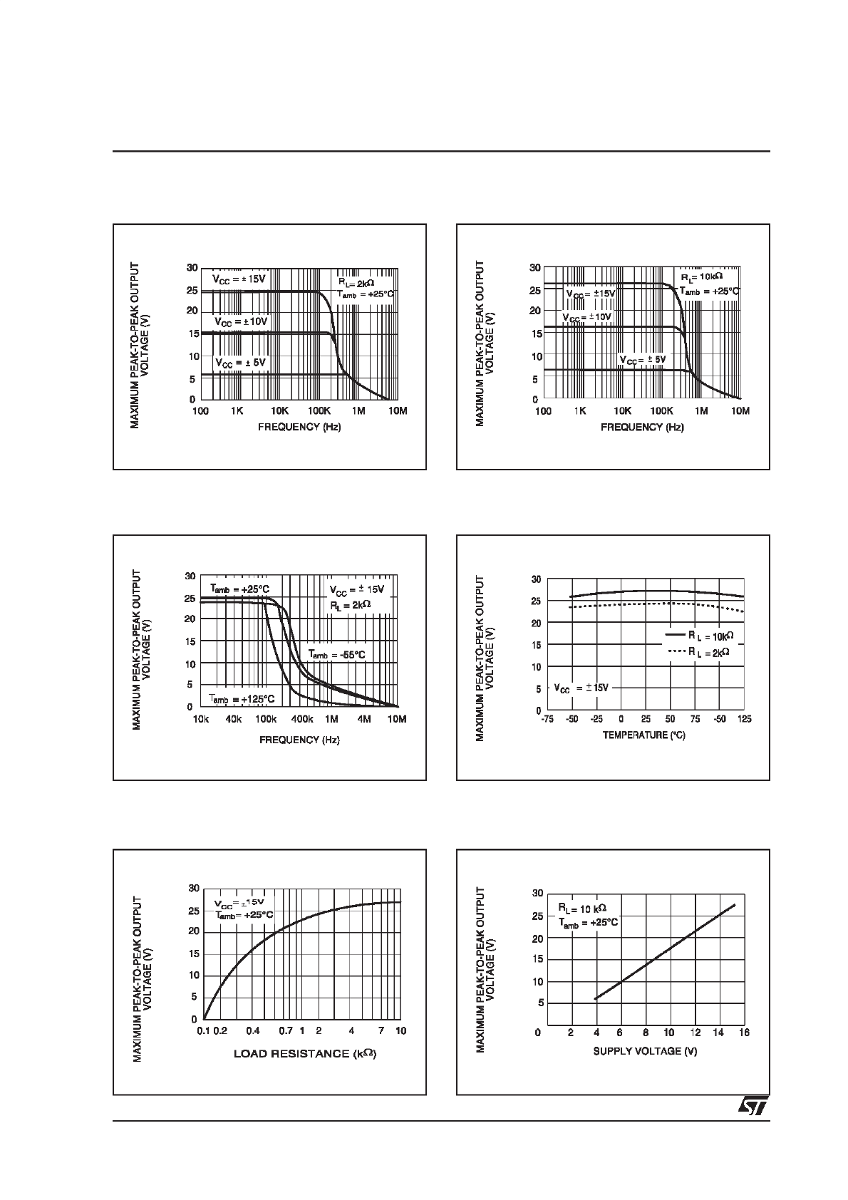
MAXIMUM PEAK-TO-PEAK OUTPUT
VOLTAGE versus FREQUENCY
MAXIMUM PEAK-TO-PEAK OUTPUT
VOLTAGE versus FREQUENCY
MAXIMUM PEAK-TO-PEAK OUTPUT
VOLTAGE versus LOAD RESISTANCE
MAXIMUM PEAK-TO-PEAK OUTPUT
VOLTAGE versus FREQUENCY
MAXIMUM PEAK-TO-PEAK OUTPUT
VOLTAGE versus FREE AIR TEMP.
MAXIMUM PEAK-TO-PEAK OUTPUT
VOLTAGE versus SUPLY VOLTAGE
LF153 - LF253 - LF353
5/9
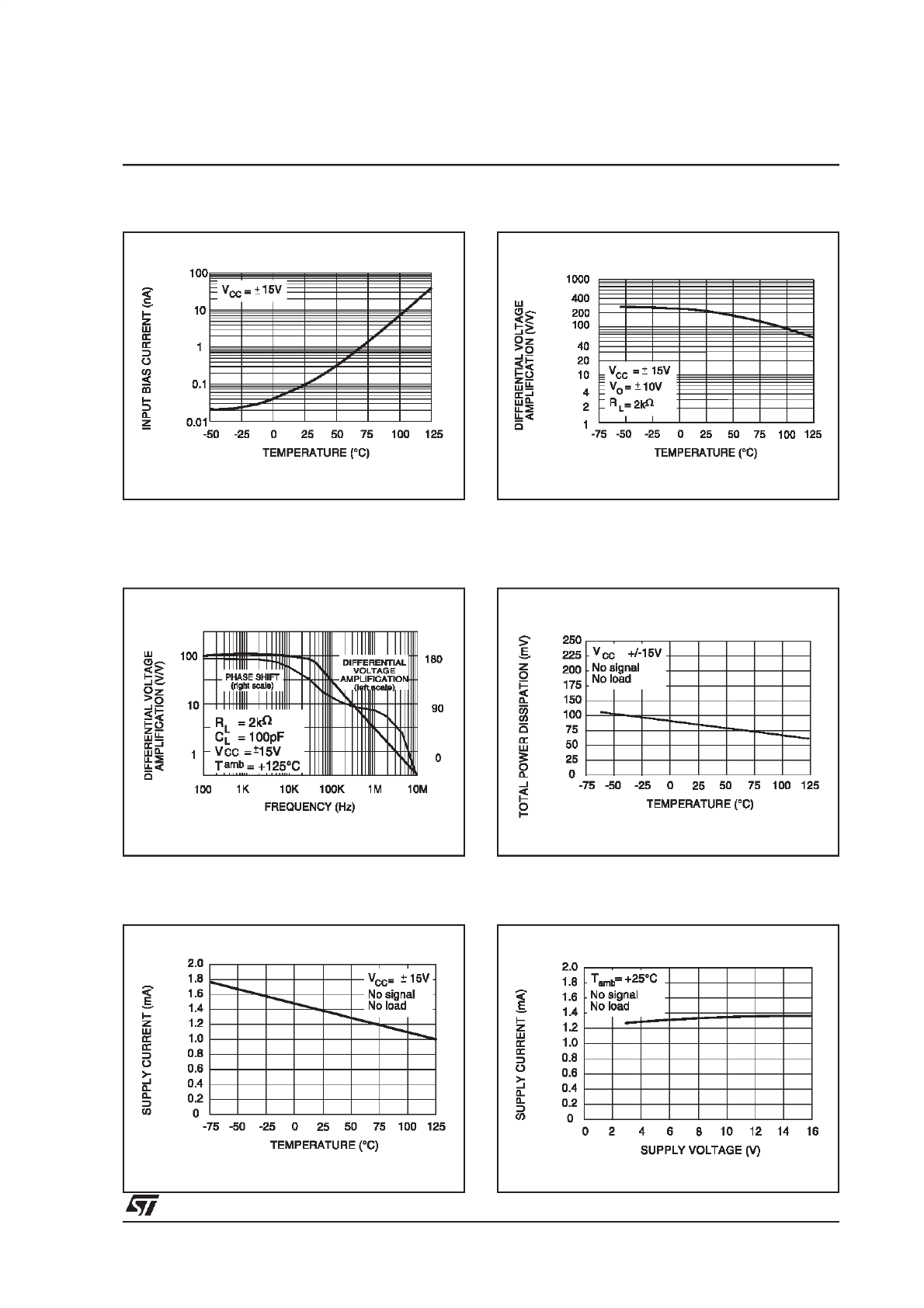
INPUT BIAS CURRENT versus FREE AIR
TEMPERATURE
LARGE SIGNAL DIFFERENTIAL VOLTAGE
AMPLIFICATION AND PHASE SHIFT versus
FREQUENCY
SUPPLY CURRENT PER AMPLIFIER versus
FREE AIR TEMPERATURE
LARGE SIGNAL DIFFERENTIAL VOLTAGE
AMPLIFICATION versus FREE AIR TEMP.
TOTAL POWER DISSIPATION versus FREE AIR
TEMPERATURE
SUPPLY CURRENT PER AMPLIFIER versus
SUPPLY VOLTAGE
LF153 - LF253 - LF353
6/9
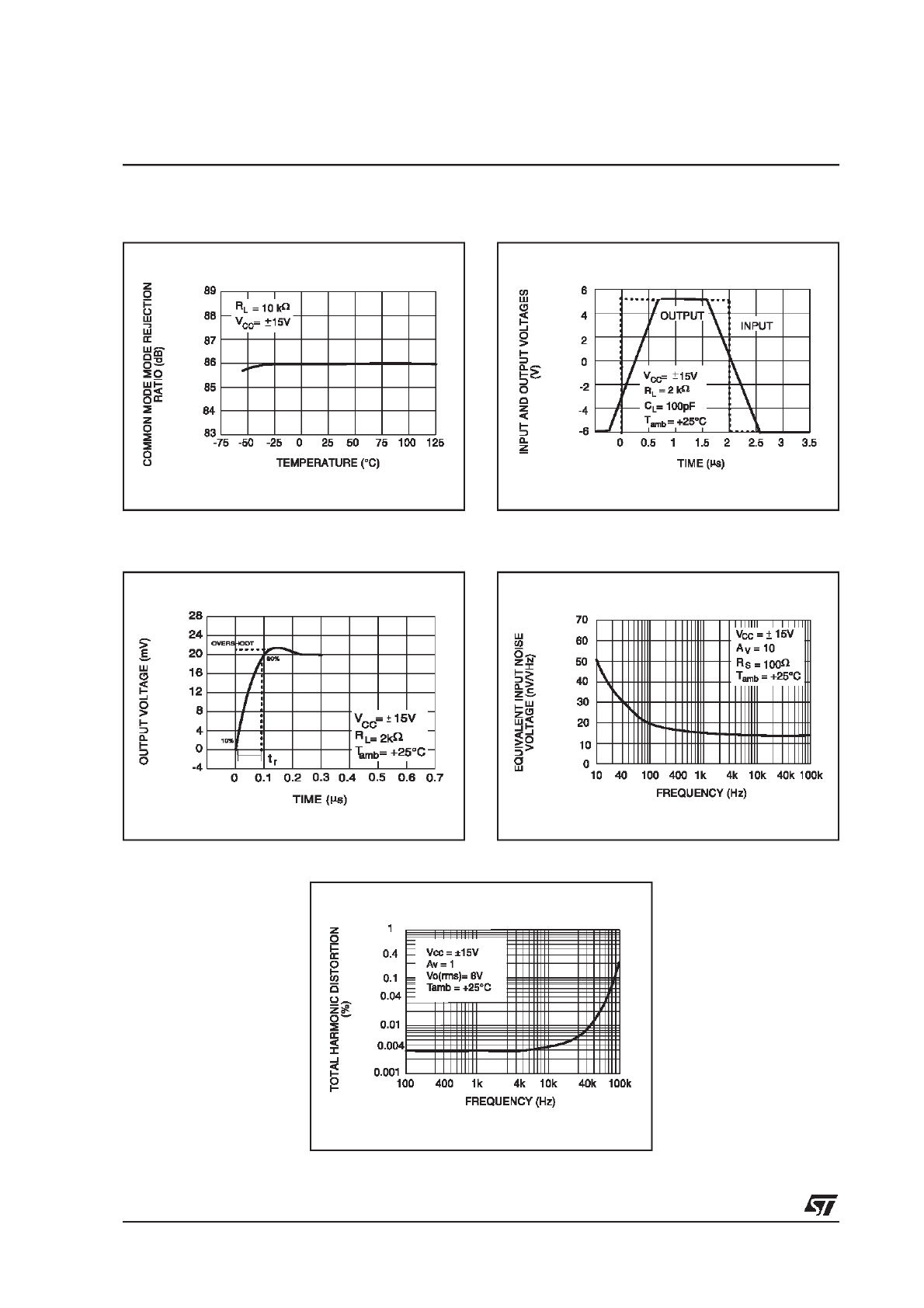
COMMON MODE REJECTION RATIO versus
FREE AIR TEMPERATURE
OUTPUT VOLTAGE versus ELAPSED TIME
VOLTAGE FOLLOWER LARGE SIGNAL PULSE
RESPONSE
EQUIVALENT INPUT NOISE VOLTAGE versus
FREQUENCY
TOTAL HARMONIC DISTORTION versus FREQUENCY
LF153 - LF253 - LF353
7/9
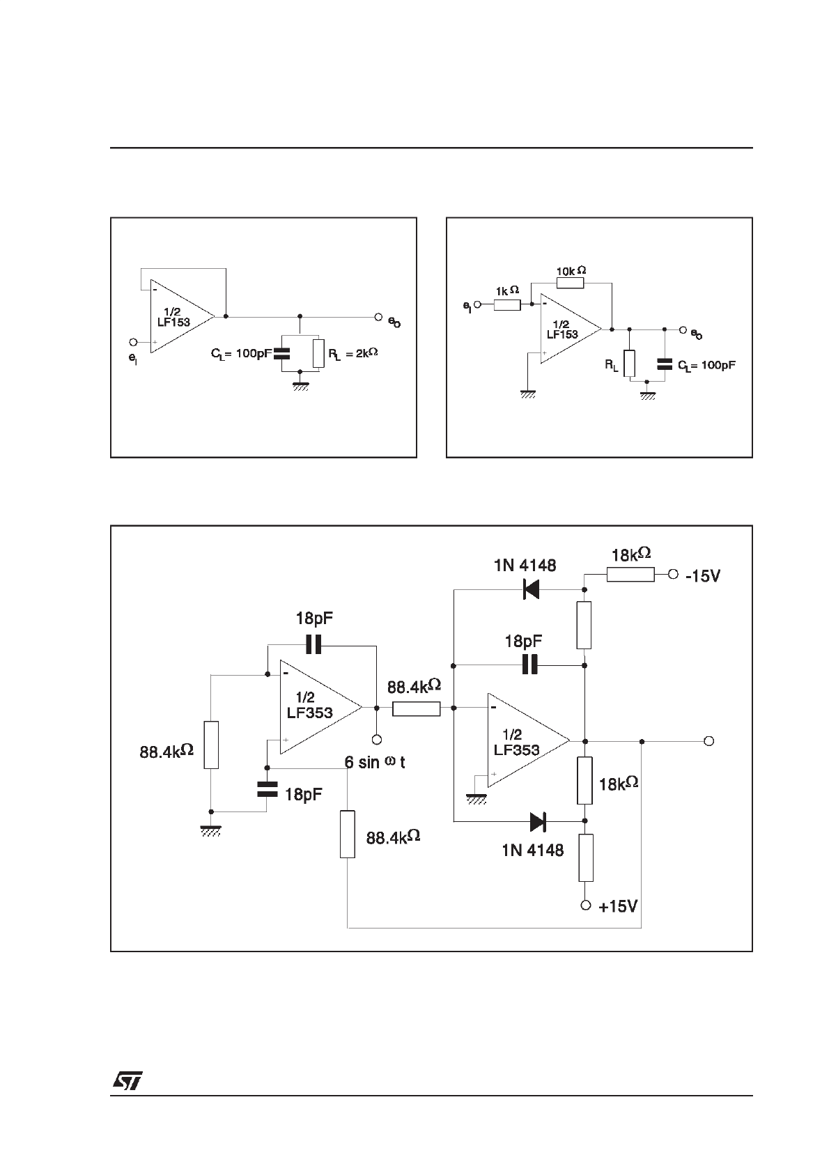
PARAMETER MEASUREMENT INFORMATION
Figure 1 : Voltage Follower
Figure 2 : Gain-of-10 inverting amplifier
TYPICAL APPLICATION
QUADRUPLE OSCILLATOR
LF153 - LF253 - LF353
8/9
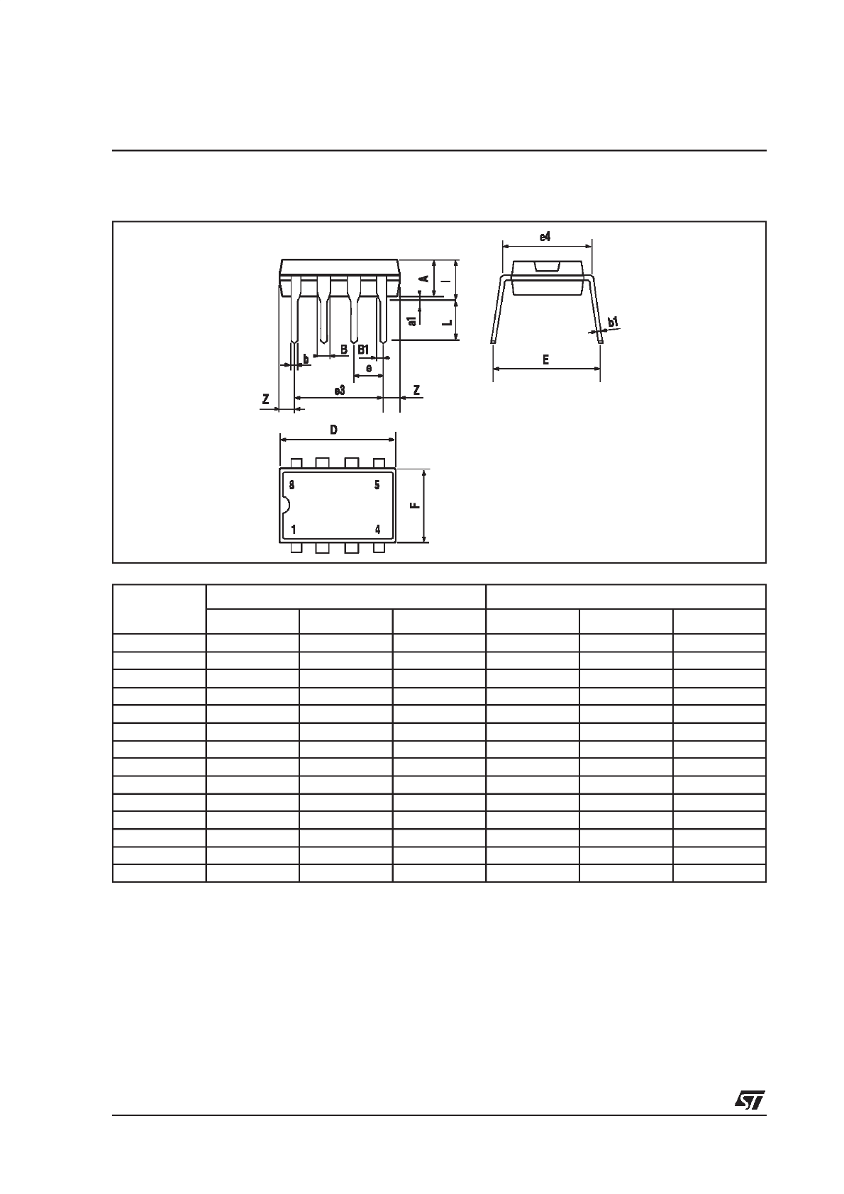
PACKAGE MECHANICAL DATA
8 PINS - PLASTIC DIP
Dim.
Millim eters
Inches
Min.
Typ.
Max.
Min.
Typ.
Max.
A
3.32
0.131
a1
0.51
0.020
B
1.15
1.65
0.045
0.065
b
0.356
0.55
0.014
0.022
b1
0.204
0.304
0.008
0.012
D
10.92
0.430
E
7.95
9.75
0.313
0.384
e
2.54
0.100
e3
7.62
0.300
e4
7.62
0.300
F
6.6
0260
i
5.08
0.200
L
3.18
3.81
0.125
0.150
Z
1.52
0.060
LF153 - LF253 - LF353
9/9
Information furn ished is believed to be accurate and reliable. However, STMicroelectronics assumes no responsibi lity for the
consequences of use of such inform ation nor for any infringement of patents or other rights of third parties which may result from
its use. No license is granted by implication or otherwise under any patent or patent right s of STMicroelectronics. Specifications
mentioned in this publicat ion are subject to change without notice. This pub lication supersedes and replaces all information
previously suppl ied. STMicroelectronics products are not authorized for use as critical components in life suppo rt devices or
systems without express written approval of STMicroelectronics.
The ST logo is a registered trademark of STMicroelectronics
2001 STMicroelectronics - Printed in Italy - All Righ ts Reserved
STMicroelectronics GROUP OF COMPANI ES
Australia - Brazil - China - Finland - France - Germany - Hong Kong - India - Italy - Japan - Malaysia - Malta - Morocco
Singapore - Spain - Sweden - Switzerland - United Kingdom
http://www .st.com
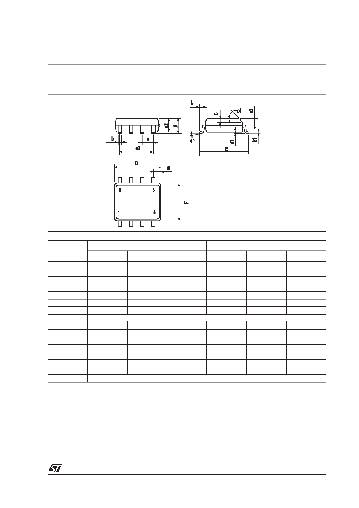
PACKAGE MECHANICAL DATA
8 PINS - PLASTIC MICROPACKAGE (SO)
Dim.
Millim eters
Inches
Min.
Typ.
Max.
Min.
Typ.
Max.
A
1.75
0.069
a1
0.1
0.25
0.004
0.010
a2
1.65
0.065
a3
0.65
0.85
0.026
0.033
b
0.35
0.48
0.014
0.019
b1
0.19
0.25
0.007
0.010
C
0.25
0.5
0.010
0.020
c1
45
°
(typ.)
D
4.8
5.0
0.189
0.197
E
5.8
6.2
0.228
0.244
e
1.27
0.050
e3
3.81
0.150
F
3.8
4.0
0.150
0.157
L
0.4
1.27
0.016
0.050
M
0.6
0.024
S
8
°
(max.)