
L6219
STEPPER MOTOR DRIVER
ABLE TO DRIVE BOTH WINDINGS OF BIPO-
LAR STEPPER MOTOR
OUTPUT CURRENT UP TO 750mA EACH
WINDING
WIDE VOLTAGE RANGE 10V TO 46V
HALF-STEP, FULL-STEP AND MICROSTEPP-
ING MODE
BUILT-IN PROTECTION DIODES
INTERNAL PWM CURRENT CONTROL
LOW OUTPUT SATURATION VOLTAGE
DESIGNED FOR UNSTABILIZED MOTOR
SUPPLY VOLTAGE
INTERNAL THERMAL SHUTDOWN
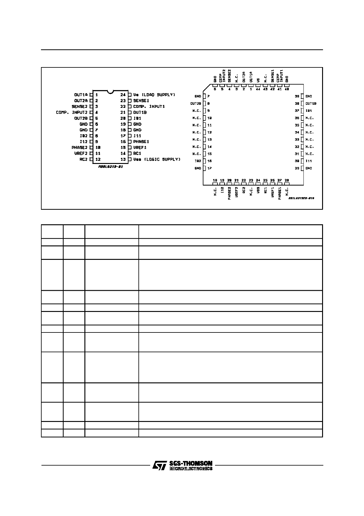
DESCRIPTION
The L6219 is a bipolar monolithic integrated cir-
cuits intended to control and drive both winding of
a bipolar stepper motor or bidirectionally control
two DC motors.
The L6219 with a few external components form
a complete control and drive circuit for LS-TTL or
microprocessor controlled stepper motor system.
The power stage is a dual full bridge capable of
sustaining 46V and including four diodes for cur-
rent recirculation.
A cross conduction protection is provided to avoid
simultaneous cross conduction during switching
current direction.
An internal pulse-width-modulation (PWM) con-
trols the output current to 750mA with peak start-
up current up to 1A.
Wide range of current control from 750mA (each
bridge) is permitted by means of two logic inputs
and an external voltage reference. A phase input
to each bridge determines the load current direc-
tion.
A thermal protection circuitry disables the outputs
if the chip temperature exceeds safe operating
limits.
December 1996
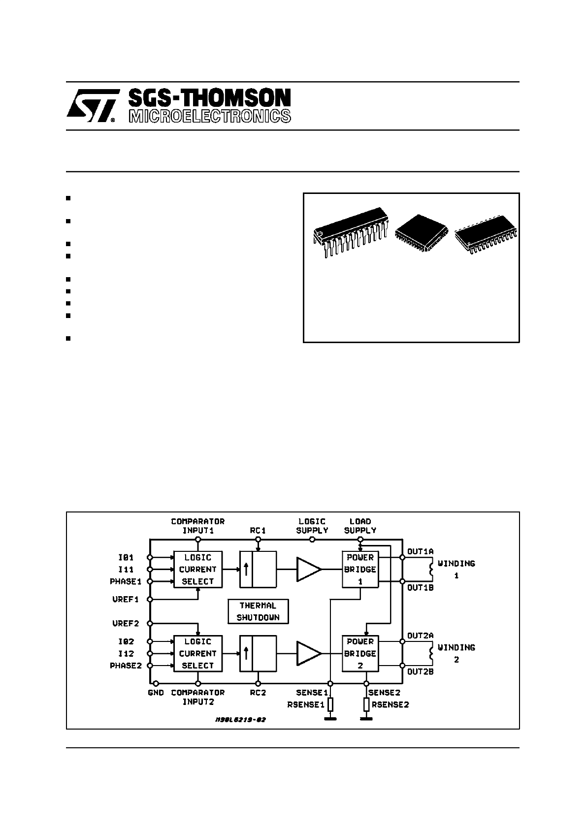
Powerdip 20+2+2
PLCC44
SO20+2+2
ORDERING NUMBERS:
L6219
L6219D
L6219DS
BLOCK DIAGRAM
1/10
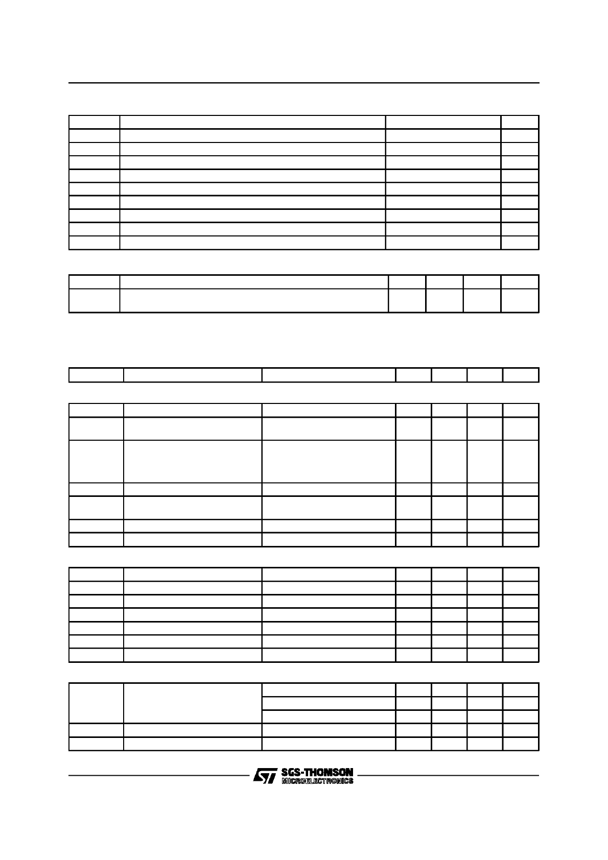
PIN FUNCTIONS
PLCC
(*)
PDIP &
SO
Name
Function
1;2
1;2
OUTPUT A
See pins 5;21
4;42
3;23
SENSE RESISTOR
Connection to Lower Emitters of Output Stage for Insertion of Current Sense
Resistor
5;41
4;22
COMPARATOR
INPUT
Input connected to the comparators. The voltage across the sense resistor is
feedback to this input throught the low pass filter RC CC. The higher power
transistors are disabled when the sense voltage exceeds the reference
voltage of the selected comparator. When this occurs the current decays for
a time set by R
T
C
T
(t
off
= 1.1 R
T
C
T
). See fig. 1.
8;38
5;21
OUTPUT B
Output Connection. The output stage is a ”H” bridge formed by four
transistors and four diodes suitable for switching applications.
6;7;17
6;19
GROUND
See pins 7;18
29;39;
40
7;18
GROUND
Ground Connection. With pins 6 and 19 also conducts heat from die to
printed circuit copper.
16;37
8;20
INPUT 0
See INPUT 1 (pins 9;17)
19;30
9;17
INPUT 1
These pins and pins 8;20 (INPUT 0) are logic inputs which select the outputs
of the comparators to set the current level. Current also depends on the
sensing resistor and reference voltage. See Funcional Description.
20;27
10;16
PHASE
This TTL-compatible logic inputs sets the direction of current flow through
the load. A high level causes current to flow from OUTPUT A (source) to
OUTPUT B (sink). A schmitt trigger on this input provides good noise
immunity and a delay circuit prevents output stage short circuits during
switching.
21;26
11;15
REFERENCE
VOLTAGE
A voltage applied to this pin sets the reference voltage of the comparators,
this determining the output current (also thus depending on R
s
and the two
inputs INPUT 0 and INPUT 1).
22;25
12;14
RC
A parallel RC network connected to this pin sets the OFF time of the higher
power transistors. The pulse generator is a monostable triggered by the
output of the comparators (t
off
= 1.1 R
T
C
T
).
24
13
V
ss
- LOGIC SUPPLY Supply Voltage Input for Logic Circuitry
44
24
Vs - LOAD SUPPLY Supply Voltage Input for the Output Stages.
(*) Pins: 3, 9,10,11,12,13,14,15,18,23,28,31,32,33,34,35,36,43 are Not Connected.
Note: ESD on GND, V
S
, V
SS
, OUT 1A and OUT 2A is guaranteed up to 1.5KV (Human Body Model, 1500
Ω
, 100pF).
PIN CONNECTIONS (Top view)
Powerdip and SO
PLCC44
L6219
2/10
ABSOLUTE MAXIMUM RATINGS
Symbol
Parameter
Value
Unit
V
S
Supply Voltage
50
V
I
o
Output Current (peak)
±
1
A
I
o
Output Current (continuous)
±
0.75
A
V
SS
Logic Supply Voltage
7
V
V
IN
Logic Input Voltage Range
-0.3 to +7
V
V
sense
Sense Output Voltage
1.5
V
T
J
Junction Temperature
+150
°
C
T
op
Operating Temperature Range
0 to 70
°
C
T
stg
Storage Temperature Range
-55 to +150
°
C
THERMAL DATA
Symbol
Description
PLCC
PDIP
SO
Unit
R
thj-case
R
thj-amb
Thermal Resistance Junction-case
Max.
Thermal Resistance Junction-ambient
Max.
12
45 (*)
14
60 (*)
18
75 (*)
°
C/W
°
C/W
(*) With minimized copper area.
ELECTRICAL CHARACTERISTICS (T
j
= 25
°
C, V
S
= 46V, V
SS
= 4.75V to 5.25V, V
REF
= 5V; unless oth-
erwise specified) See fig. 3.
Symbol
Parameter
Test Condition
Min.
Typ.
Max.
Unit
OUTPUT DRIVERS (OUT
A
or OUT
B
)
V
S
Motor Supply Range
10
46
V
I
CEX
Output Leakage Current
V
OUT
= Vs
V
OUT
= 0
-
-
<1
<-1
50
-50
µ
A
µ
A
V
CE(sat)
Output Saturation Voltage
Sink Driver, I
OUT
= +500mA
Sink Driver, I
OUT
= +750mA
Source Driver, I
OUT
= -500mA
Source Driver, I
OUT
= -750mA
-
-
-
-
0.3
0.7
1.1
1.3
0.6
1
1.4
1.6
V
V
V
V
I
R
Clamp Diode Leakage Current
V
R
= 50V
-
<1
50
µ
A
V
F
Clamp Diode Forward Voltage
Sink Diode
Source Diode I
F
=750mA
1
1
1.5
1.5
V
V
I
S(on)
Driver Supply Current
Both Bridges ON, No Load
-
8
15
mA
I
S(off)
Driver Supply Current
Both Bridges OFF
-
6
10
mA
CONTROL LOGIC
V
IN(H)
Input Voltage
All Inputs
2.4
-
-
V
V
IN(L)
Input Voltage
All Inputs
-
-
0.8
V
I
IN(H)
Input Current
VIN = 2.4V
-
<1
20
µ
A
I
IN(L)
Input Current
VIN = 0.84V
-
-3
-200
µ
A
V
REF
Reference Voltage
Operating
1.5
-
7.5
V
I
SS(ON)
Total Logic Supply Current
I
o
= I
1
= 0.8V, No Load
-
64
74
mA
I
SS(OFF)
Total Logic Supply Current
I
o
= I
1
= 2.4V, No Load
-
10
14
mA
COMPARATORS
V
REF
/ V
sense
Current Limit Threshold (at trip
point
I
o
= I
1
= 0.8V
9.5
10
10.5
-
I
o
= 2.4V, I
1
= 0.8V
13.5
15
16.5
-
I
o
= 0.8V, I
1
= 2.4V
25.5
30
34.5
-
t
off
Cutoff Time
Rt = 56K
Ω
C
t
= 820pF
-
50
s
t
d
Turn Off Delay
Fig. 1
-
1
s
µ
µ
L6219
3/10
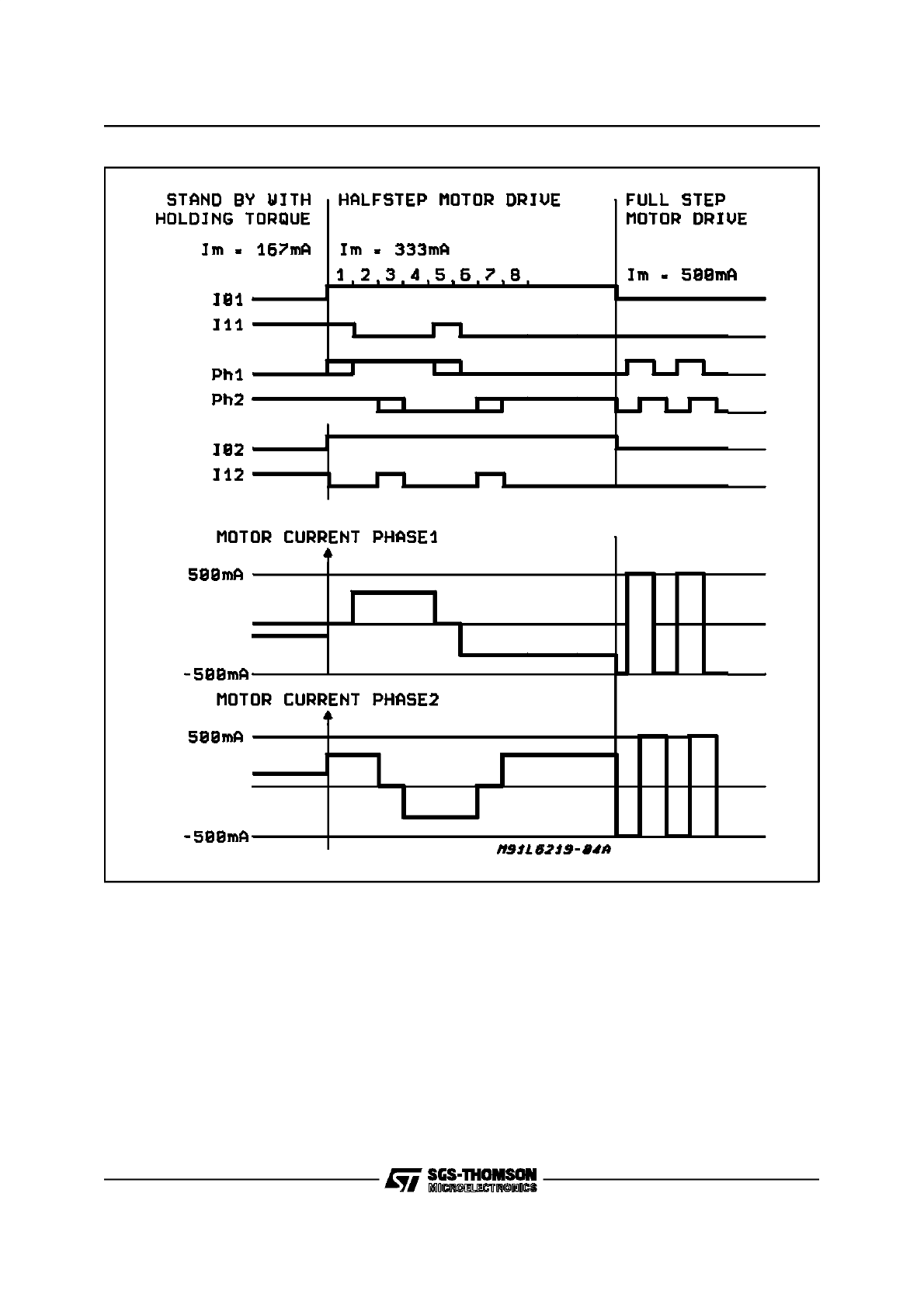
FUNCTIONAL DESCRIPTION
The circuit is intended to drive both windings of a
bipolar stepper motor.
The peak current control is generated through
switch mode regulation.
There is a choice of three different current levels
with the two logic inputs I
01
- I
11
for winding 1 and
I
02
- I
12
for winding 2.
The current can also be switched off completely
Input Logic (I
0
and I
1
)
The current level in the motor winding is selected
with these inputs. (See fig. 2)
If any of the logic inputs is left open, the circuit will
treat it has a high level input.
I
o
I
1
Current Level
H
L
H
L
H
H
L
L
No Current
Low Current 1/3 I
o
max
Medium Current 2/3 I
o
max
Maximum Current I
o
max
Phase
This input determines the direction of current flow
in the windings, depending on the motor connec-
tions. The signal is fed through a Schmidt-trigger
for noise immunity, and through a time delay in
order to guarantee that no short-circuit occurs in
the output stage during phase-shift.
High level on the PHASE input causes the motor
current flow from Out A through the winding to
Out B
Current Sensor
This part contains a current sensing resistor (R
S
),
a low pass filter (R
C
, C
C
) and three comparators.
Only one comparator is active at a time. It is acti-
vated by the input logic according to the current
level chosen with signals I
o
and I
1
.
The motor current flows through the sensing re-
sistor R
S
.
When the current has increased so that the volt-
age across R
S
becomes higher than the refer-
ence voltage on the other comparator input, the
comparator goes high, which triggers the pulse
generator.
The max peak current I
max
can be defined by:
I
max
=
V
ref
10 R
s
Figure 1
ELECTRICAL CHARACTERISTICS (Continued)
Symbol
Parameter
Test Condition
Min.
Typ.
Max.
Unit
PROTECTION
T
J
Thermal Shutdown Temperature
-
170
-
°
C
L6219
4/10
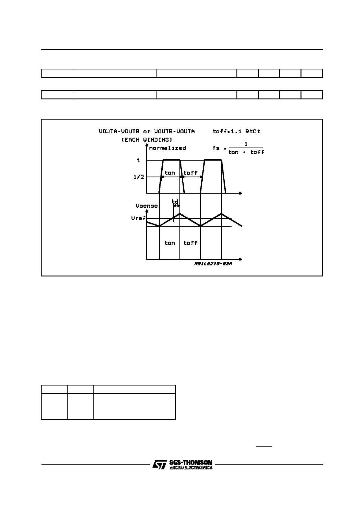
Single-pulse Generator
The pulse generator is a monostable triggered on
the positive going edge of the comparator output.
The monostable output is high during the pulse
time, t
off
, which is determined by the time compo-
nents R
t
and C
t
.
t
off
= 1.1
•
R
t
C
t
The single pulse switches off the power feed to
the motor winding, causing the winding current to
decrease during t
off
.
If a new trigger signal should occur during t
off
, it is
ignored.
Output Stage
The output stage contains four Darlington transis-
tors (source drivers) four saturated transistors
(sink drivers) and eight diodes, connected in two
H bridge.
The source transistors are used to switch the
power supplied to the motor winding, thus driving
a constant current through the winding.
It should be noted however, that is not permitted
to short circuit the outputs.
Internal circuitry is added in order to increase the
accuracy of the motor current particularly with low
current levels.
Figure 2: Principle Operating Sequence
L6219
5/10
V
S
, V
SS
, V
Ref
The circuit will stand any order of turn-on or turn-
off the supply voltages V
S
and V
SS
. Normal dV/dt
values are then assumed.
Preferably, V
Ref
should be tracking V
SS
during
power-on and power-off if V
S
is established.
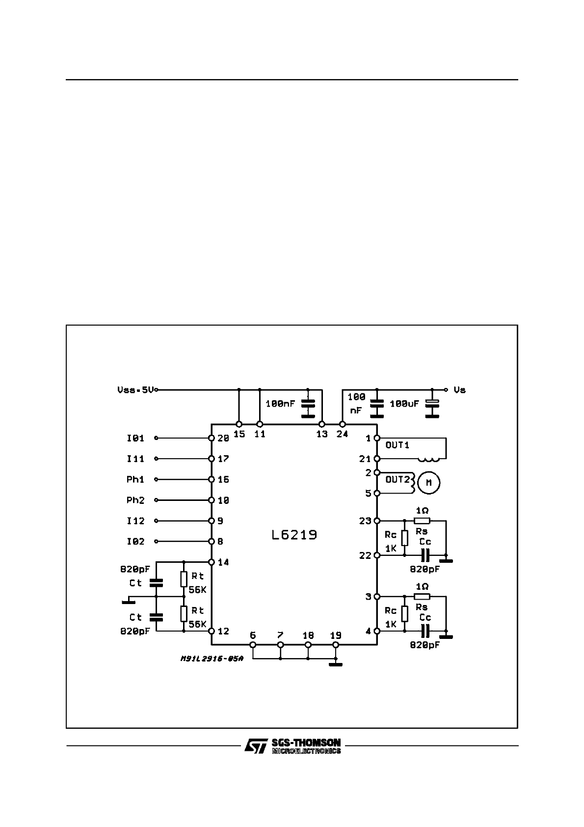
APPLICATION INFORMATIONS (Note 1)
Some stepper motors are not designed for contin-
uous operation at maximum current. As the circuit
drives a constant current through the motor, its
temperature might increase exceedingly both at
low and high speed operation.
Also, some stepper motors have such high core
losses that they are not suited for switch mode
current regulation.
Unused inputs should be connected to proper
voltage levels in order to get the highest noise im-
munity.
As the circuit operates with switch mode current
regulation,
interference
generation
problems
might arise in some applications. A good measure
might then be to decouple the circuit with a 100nF
capacitor, located near the package between
power line and ground.
The ground lead between R
s
, and circuit GND
should be kept as short as possible.
A typical Application Circuit is shown in Fig. 3.
Note that C
t
must be NPO type or similar else.
To sense the winding current, paralleled metal
film resistors are recommended (R
s
)
Note 1 - Other information is available as ”Smart
Power Development System”:
Test board HWL6219 (Stepper driver)
Software SWL6219 (Floppy disc)
Figure 3: Typical Application Circuit. (Pin out referred to DIP24 package)
L6219
6/10
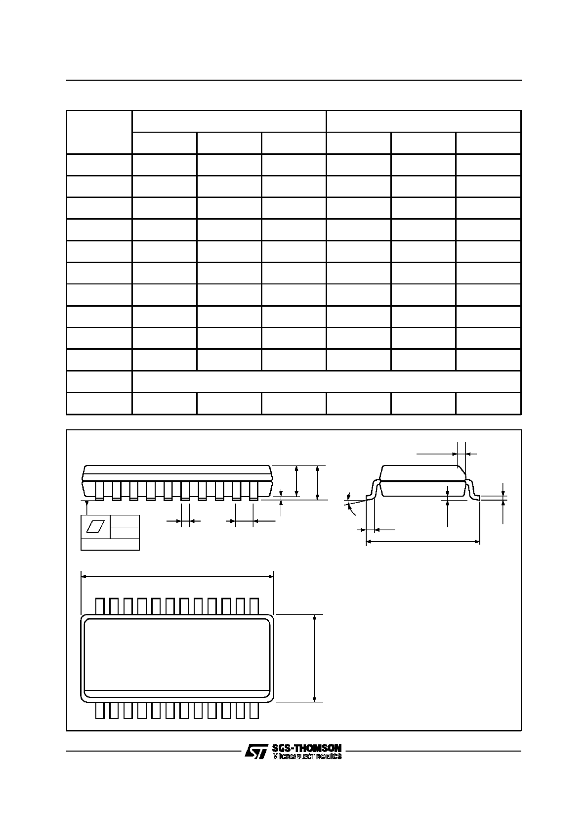
DIM.
mm
inch
MIN.
TYP.
MAX.
MIN.
TYP.
MAX.
A
4.320
0.170
A1
0.380
0.015
A2
3.300
0.130
B
0.410
0.460
0.510
0.016
0.018
0.020
B1
1.400
1.520
1.650
0.055
0.060
0.065
c
0.200
0.250
0.300
0.008
0.010
0.012
D
31.62
31.75
31.88
1.245
1.250
1.255
E
7.620
8.260
0.300
0.325
e
2.54
0.100
E1
6.350
6.600
6.860
0.250
0.260
0.270
e1
7.620
0.300
L
3.180
3.430
0.125
0.135
M
0
°
min, 15
°
max.
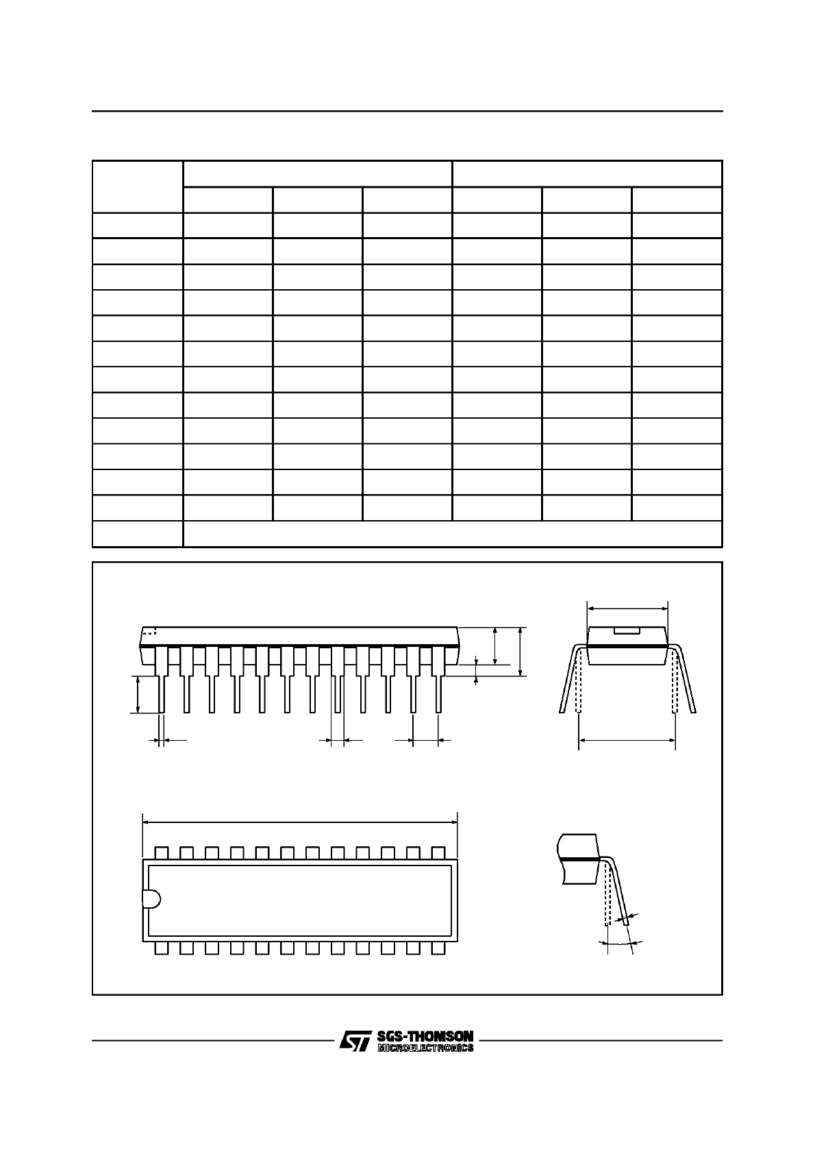
DIP24 PACKAGE MECHANICAL DATA
A1
B
e
B1
D
13
12
24
1
L
A
e1
A2
c
E1
SDIP24L
M
L6219
7/10
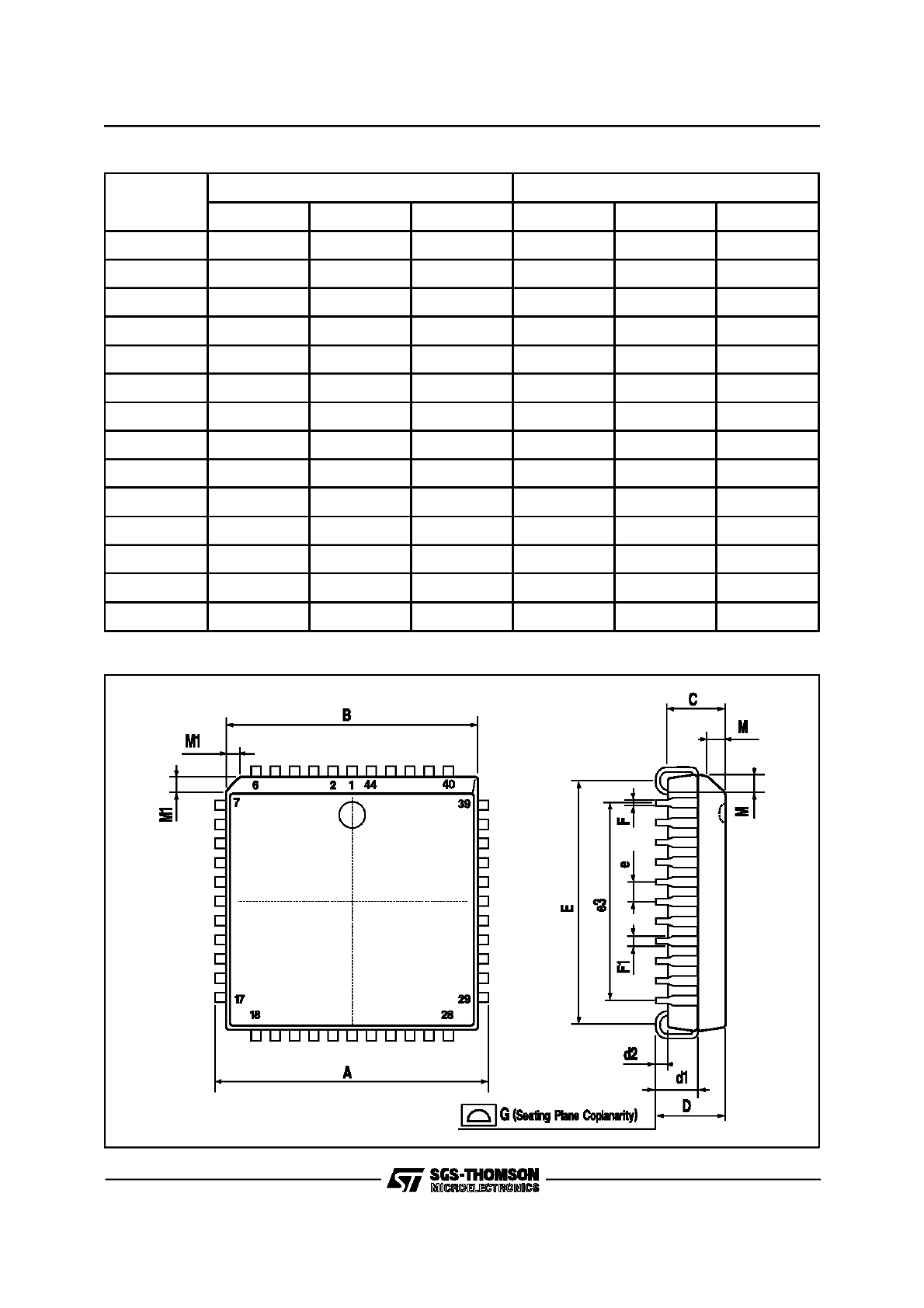
PLCC44 PACKAGE MECHANICAL DATA
DIM.
mm
inch
MIN.
TYP.
MAX.
MIN.
TYP.
MAX.
A
17.4
17.65
0.685
0.695
B
16.51
16.65
0.650
0.656
C
3.65
3.7
0.144
0.146
D
4.2
4.57
0.165
0.180
d1
2.59
2.74
0.102
0.108
d2
0.68
0.027
E
14.99
16
0.590
0.630
e
1.27
0.050
e3
12.7
0.500
F
0.46
0.018
F1
0.71
0.028
G
0.101
0.004
M
1.16
0.046
M1
1.14
0.045
P027B
L6219
8/10
DIM.
mm
inch
MIN.
TYP.
MAX.
MIN.
TYP.
MAX.
A
2.35
2.65
0.093
0.104
A1
0.10
0.30
0.004
0.012
A2
2.55
0.100
B
0.33
0.51
0.013
0.0200
C
0.23
0.32
0.009
0.013
D
15.20
15.60
0.598
0.614
E
7.40
7.60
0.291
0.299
e
1.27
0,050
H
10.0
10.65
0.394
0.419
h
0.25
0.75
0.010
0.030
k
0
°
(min.), 8
°
(max.)
L
0.40
1.27
0.016
0.050
B
e
A2
A
1
12
13
24
D
L
H
A1
C
E
K
h x 45?
SO24
Seating Plane
0.10mm
.004
A1
SO24 PACKAGE MECHANICAL DATA
L6219
9/10

Information furnished is believed to be accurate and reliable. However, SGS-THOMSON Microelectronics assumes no responsibility for the
consequences of use of such information nor for any infringement of patents or other rights of third parties which may result from its use. No
license is granted by implication or otherwise under any patent or patent rights of SGS-THOMSON Microelectronics. Specification mentioned
in this publication are subject to change without notice. This publication supersedes and replaces all information previously supplied. SGS-
THOMSON Microelectronics products are not authorized for use as critical components in life support devices or systems without express
written approval of SGS-THOMSON Microelectronics.
1996 SGS-THOMSON Microelectronics – Printed in Italy – All Rights Reserved
SGS-THOMSON Microelectronics GROUP OF COMPANIES
Australia - Brazil - Canada - China - France - Germany - Hong Kong - Italy - Japan - Korea - Malaysia - Malta - Morocco - The Netherlands -
Singapore - Spain - Sweden - Switzerland - Taiwan - Thailand - United Kingdom - U.S.A.
L6219
10/10