
L297
L297D
STEPPER MOTOR CONTROLLERS
NORMAL/WAWE DRIVE
HALF/FULL STEP MODES
CLOCKWISE/ANTICLOCKWISE DIRECTION
SWITCHMODE LOAD CURRENT REGULA-
TION
PROGRAMMABLE LOAD CURRENT
FEW EXTERNAL COMPONENTS
RESET INPUT & HOME OUTPUT
ENABLE INPUT
DESCRIPTION
The L297/A/D Stepper Motor Controller IC gener-
ates four phase drive signals for two phase bipolar
and four phase unipolar step motors in microcom-
puter-controlled applications. The motor can be
driven in half step, normal and wawe drive modes
and on-chip PWM chopper circuits permit switch-
mode control of the current in the windings. A
August 1996
Symbol
Parameter
Value
Unit
V
s
Supply voltage
10
V
V
i
Input signals
7
V
P
tot
Total power dissipation (T
amb
= 70
°
C)
1
W
T
stg
, T
j
Storage and junction temperature
-40 to + 150
°
C
ABSOLUTE MAXIMUM RATINGS
feature of this device is that it requires only clock,
direction and mode input signals. Since the phase
are generated internally the burden on the micro-
processor, and the programmer, is greatly reduced.
Mounted in DIP20 and SO20 packages, the L297
can be used with monolithic bridge drives such as
the L298N or L293E, or with discrete transistors
and darlingtons.
TWO PHASE BIPOLAR STEPPER MOTOR CONTROL CIRCUIT
DIP20
SO20
ORDERING NUMBERS : L297 (DIP20)
L297D (SO20)
1/11
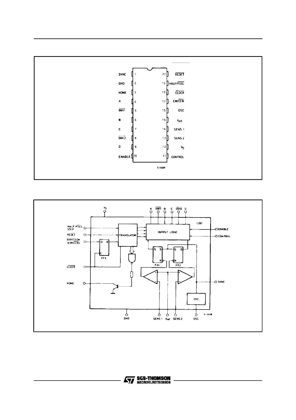
PIN CONNECTION (Top view)
BLOCK DIAGRAM (L297/L297D)
2/11
L297
L297D
L297-L297D
N
°
NAME
FUNCTION
1
SYNC
Output of the on-chip chopper oscillator.
The SYNC connections The SYNC connections of all L297s to be
synchronized are connected together and the oscillator
components are omitted on all but one. If an external clock source
is used it is injected at this terminal.
2
GND
Ground connection.
3
HOME
Open collector output that indicates when the L297 is in its initial
state (ABCD = 0101).
The transistor is open when this signal is active.
4
A
Motor phase A drive signal for power stage.
5
INH1
Active low inhibit control for driver stage of A and B phases.
When a bipolar bridge is used this signal can be used to ensure
fast decay of load current when a winding is de-energized. Also
used by chopper to regulate load current if CONTROL input is low.
6
B
Motor phase B drive signal for power stage.
7
C
Motor phase C drive signal for power stage.
8
INH2
Active low inhibit control for drive stages of C and D phases.
Same functions as INH1.
9
D
Motor phase D drive signal for power stage.
10
ENABLE
Chip enable input. When low (inactive) INH1, INH2, A, B, C and D
are brought low.
11
CONTROL
Control input that defines action of chopper.
When low chopper acts on INH1 and INH2; when high chopper
acts on phase lines ABCD.
12
V
s
5V supply input.
13
SENS
2
Input for load current sense voltage from power stages of phases
C and D.
14
SENS
1
Input for load current sense voltage from power stages of phases
A and B.
15
V
ref
Reference voltage for chopper circuit. A voltage applied to this pin
determines the peak load current.
16
OSC
An RC network (R to V
CC
, C to ground) connected to this terminal
determines the chopper rate. This terminal is connected to ground
on all but one device in synchronized multi - L297 configurations. f
≅
1/0.69 RC
17
CW/CCW
Clockwise/counterclockwise direction control input.
Physical direction of motor rotation also depends on connection
of windings.
Synchronized internally therefore direction can be changed at any
time.
18
CLOCK
Step clock. An active low pulse on this input advances the motor
one increment. The step occurs on the rising edge of this signal.
PIN FUNCTIONS - L297/L297D
3/11
L297-L297D
N
°
NAME
FUNCTION
19
HALF/FULL
Half/full step select input. When high selects half step operation,
when low selects full step operation. One-phase-on full step mode
is obtained by selecting FULL when the L297’s translator is at an
even-numbered state.
Two-phase-on full step mode is set by selecting FULL when the
translator is at an odd numbered position. (The home position is
designate state 1).
20
RESET
Reset input. An active low pulse on this input restores the
translator to the home position (state 1, ABCD = 0101).
PIN FUNCTIONS - L297/L297D (continued)
CIRCUIT OPERATION
The L297 is intended for use with a dual bridge
driver, quad darlington array or discrete power
devices in step motor driving applications. It re-
ceives step clock, direction and mode signals from
the systems controller (usually a microcomputer
chip) and generates control signals for the power
stage.
The principal functions are a translator, which gen-
erates the motor phase sequences, and a dual
PWM chopper circuit which regulates the current in
the motor windings.The translator generatesthree
different sequences, selected by the HALF/FULL
input. These are normal (two phases energised),
wave drive (one phase energised) and half-step
(alternately one phase energised/two phases en-
ergised). Two inhibit signals are also generated by
the L297 in half step and wave drive modes. These
signals, which connect directly to the L298’senable
inputs, are intended to speed current decay when
a winding is de-energised. When the L297 is used
to drive a unipolar motor the chopper acts on these
lines.
An input called CONTROL determines whether the
chopper will act on the phase lines ABCD or the
inhibit lines INH1 and INH2. When the phase lines
are chopped the non-active phase line of each pair
(AB or CD) is activated (rather than interrupting the
line then active).In L297 + L298 configurationsthis
technique reduces dissipation in the load current
sense resistors.
A common on-chip oscillator drives the dual chop-
per.It suppliespulses at the chopper rate which set
the two flip-flops FF1 and FF2. When the current in
a winding reaches the programmed peak value the
voltage across the sense resistor (connected to
one of the sense inputs SENS
1
or SENS
2
) equals
V
ref
and the corresponding comparator resets its
flip flop, interrupting the drive current until the next
oscillator pulse arrives. The peak current for both
windingsis programmedby a voltage divideron the
V
ref
input.
Ground noise problems in multiple configurations
can be avoided by synchronising the chopper os-
cillators. This is done by connecting all the SYNC
pins together, mounting the oscillator RC network
on one device only and grounding the OSC pin on
all other devices.
Symbol
Parameter
DIP20
SO20
Unit
R
th-j-amb
Thermal resistance junction-ambient
max
80
100
°
C/W
THERMAL DATA
4/11
L297-L297D
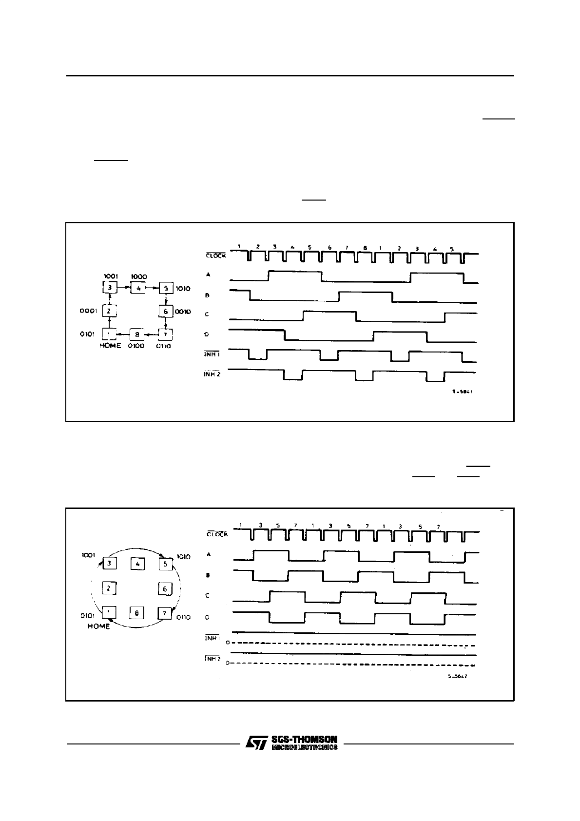
MOTOR DRIVING PHASE SEQUENCES
The L297’s translator generates phase sequences
for normal drive, wave drive and half step modes.
The state sequences and output waveforms for
these three modes are shown below. In all cases
the translator advances on the low to high transis-
tion of CLOCK.
Clockwise rotation is indicate; for anticlockwise ro-
tation the sequences are simply reversed RESET
restores the translator to state 1, where ABCD =
0101.
HALF STEP MODE
Half step mode is selected by a high level on the HALF/FULL input.
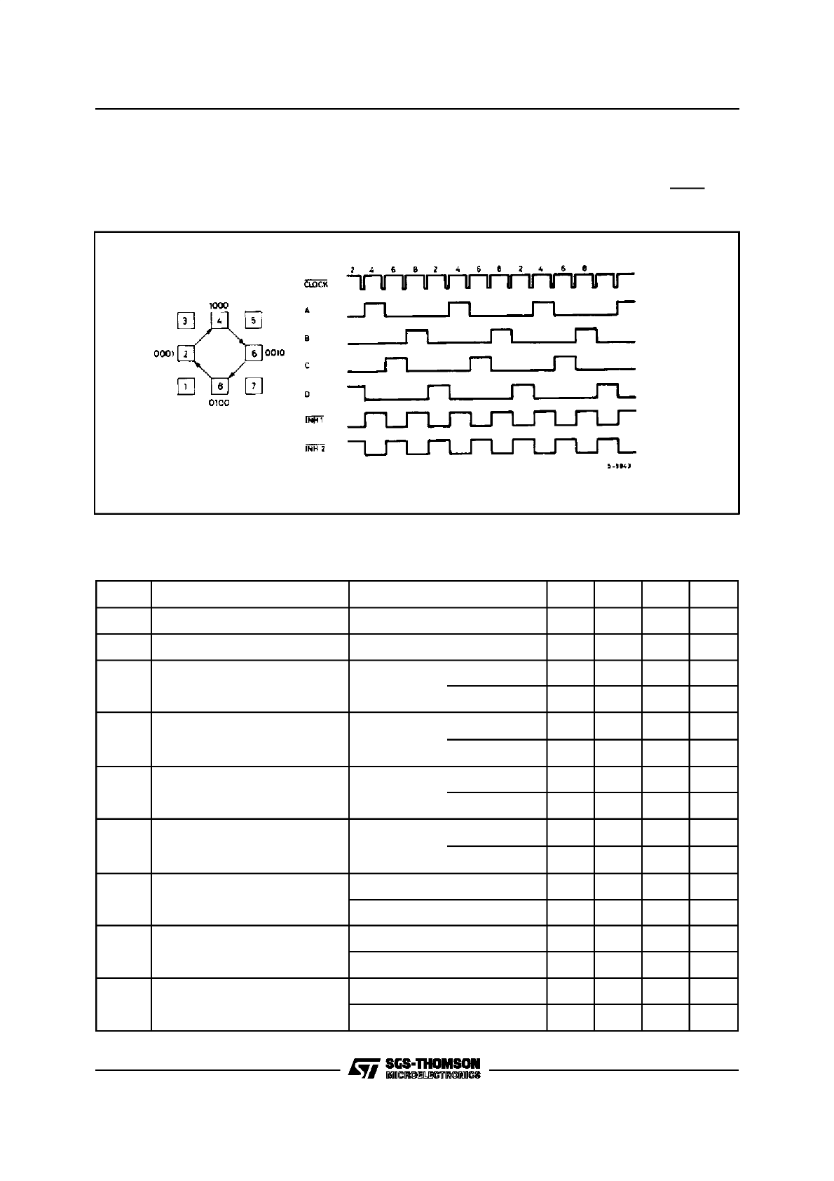
NORMAL DRIVE MODE
Normal drive mode (also called ”two-phase-on” drive) is selected by a low level on the HALF/FULL input
when the translator is at an odd numbered state (1, 3, 5 or 7). In this mode the INH1 and INH2 outputs
remain high throughout.
5/11
L297-L297D
MOTOR DRIVING PHASE SEQUENCES (continued)
WAVE DRIVE MODE
Wave drive mode (also called ”one-phase-on” drive) is selected by a low level on the HALF/FULL input
when the translator is at an even numbered state (2, 4, 6 or 8).
Symbol
Parameter
Test conditions
Min.
Typ
Max.
Unit
V
s
Supply voltage (pin 12)
4.75
7
V
I
s
Quiescent supply current (pin 12)
Outputs floating
50
80
mA
V
i
Input voltage
(pin 11, 17, 18, 19, 20)
Low
0.6
V
High
2
V
s
V
I
i
Input current
(pin 11, 17, 18, 19, 20)
V
i
= L
100
µ
A
V
i
= H
10
µ
A
V
en
Enable input voltage (pin 10)
Low
1.3
V
High
2
V
s
V
I
en
Enable input current (pin 10)
V
en
= L
100
µ
A
V
en
= H
10
µ
A
V
o
Phase output voltage
(pins 4, 6, 7, 9)
I
o
= 10mA
V
OL
0.4
V
I
o
= 5mA
V
OH
3.9
V
V
inh
Inhibit output voltage (pins 5, 8)
I
o
= 10mA
V
inh L
0.4
V
I
o
= 5mA
V
inh H
3.9
V
V
SYNC
Sync Output Voltage
I
o
= 5mA
V
SYNC H
3.3
V
I
o
= 5mA
V
SYNC V
0.8
ELECTRICAL CHARACTERISTICS (Refer to the block diagram T
amb
= 25
°
C, V
s
= 5V unless otherwise
specified)
6/11
L297-L297D
Symbol
Parameter
Test conditions
Min.
Typ
Max.
Unit
I
leak
Leakage current (pin 3)
V
CE
= 7 V
1
µ
A
V
sat
Saturation voltage (pin 3)
I = 5 mA
0.4
V
V
off
Comparators offset voltage
(pins 13, 14, 15)
V
ref
= 1 V
5
mV
I
o
Comparator bias current
(pins 13, 14, 15)
-100
10
µ
A
V
ref
Input reference voltage (pin 15)
0
3
V
t
CLK
Clock time
0.5
µ
s
t
S
Set up time
1
µ
s
t
H
Hold time
4
µ
s
t
R
Reset time
1
µ
s
t
RCLK
Reset to clock delay
1
µ
s
ELECTRICAL CHARACTERISTICS (continued)
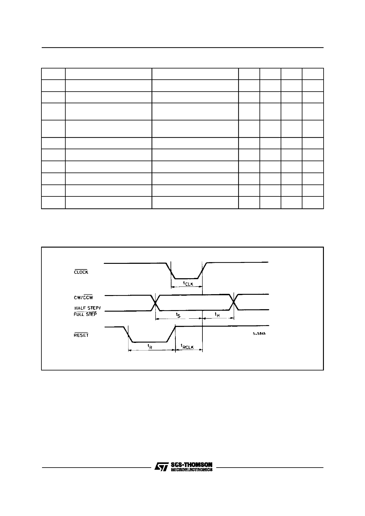
Figure 1.
7/11
L297-L297D
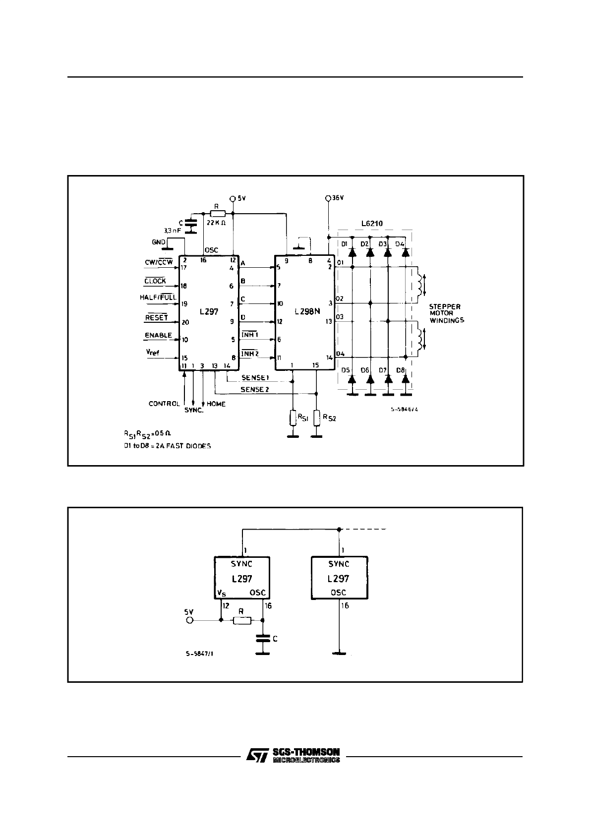
APPLICATION INFORMATION
TWO PHASE BIPOLAR STEPPER MOTOR CONTROL CIRCUIT
This circuit drives bipolar stepper motors with winding currents up to 2A. The diodes are fast 2A types.
Figure 2.
Figure 3 : Synchronising L297s
8/11
L297-L297D
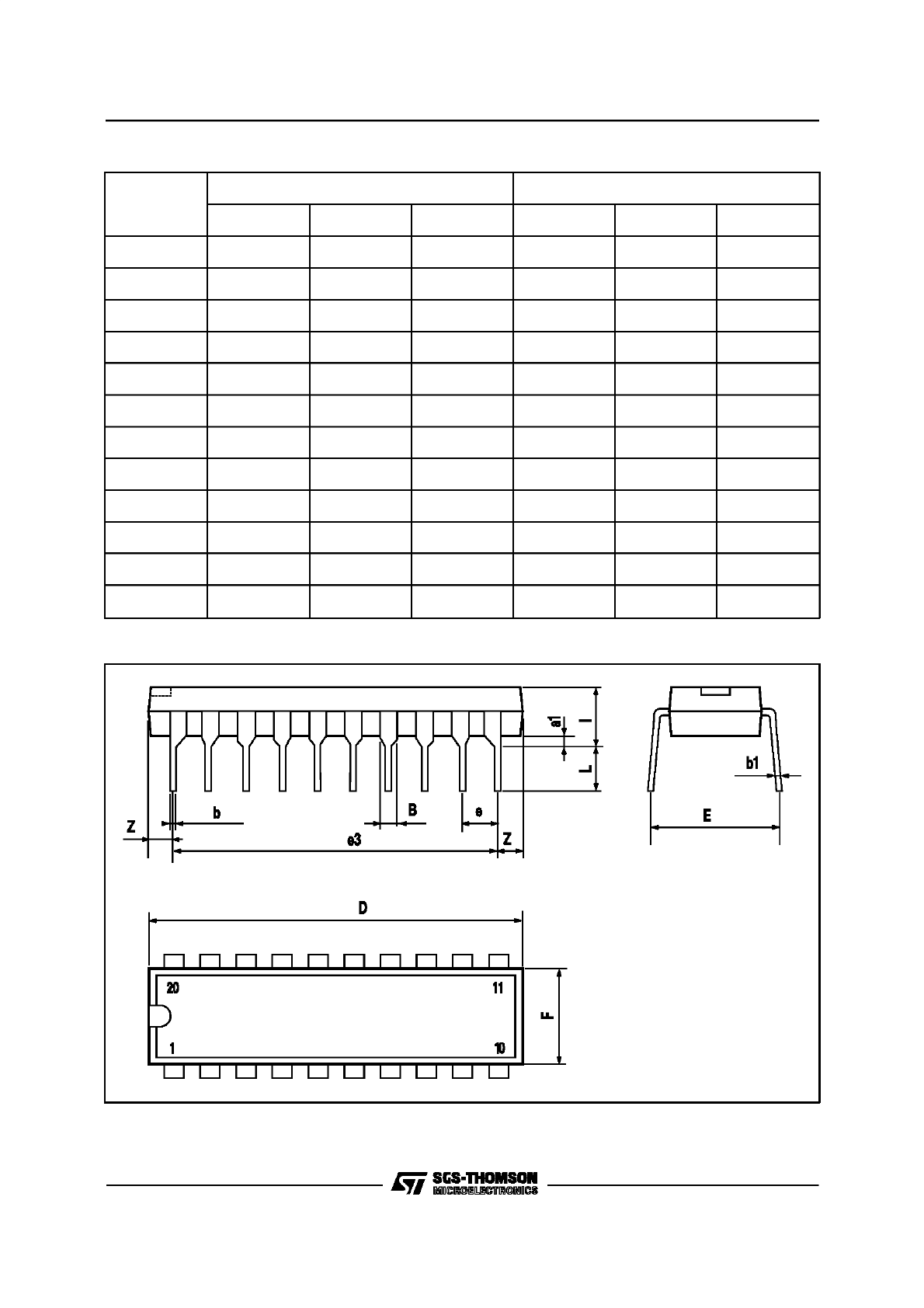
DIM.
mm
inch
MIN.
TYP.
MAX.
MIN.
TYP.
MAX.
a1
0.254
0.010
B
1.39
1.65
0.055
0.065
b
0.45
0.018
b1
0.25
0.010
D
25.4
1.000
E
8.5
0.335
e
2.54
0.100
e3
22.86
0.900
F
7.1
0.280
I
3.93
0.155
L
3.3
0.130
Z
1.34
0.053
DIP20 PACKAGE MECHANICAL DATA
9/11
L297-L297D
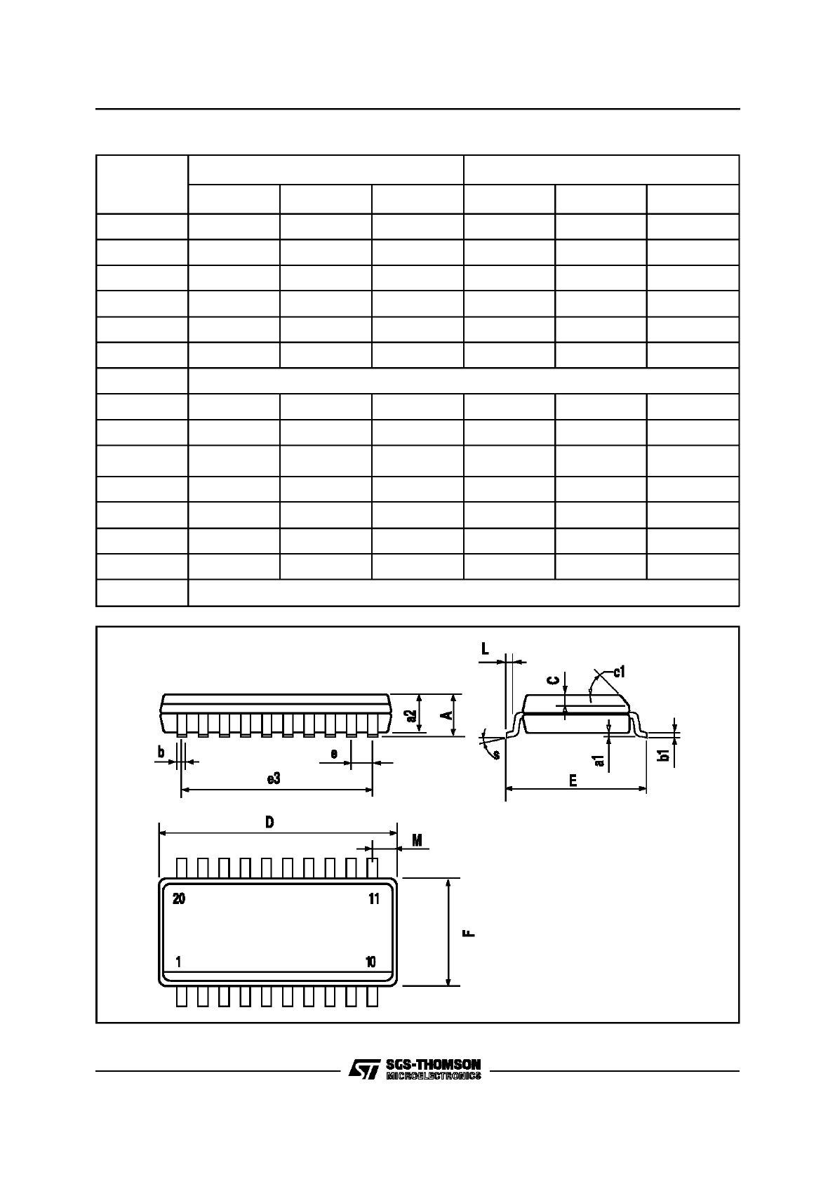
DIM.
mm
inch
MIN.
TYP.
MAX.
MIN.
TYP.
MAX.
A
2.65
0.104
a1
0.1
0.3
0.004
0.012
a2
2.45
0.096
b
0.35
0.49
0.014
0.019
b1
0.23
0.32
0.009
0.013
C
0.5
0.020
c1
45 (typ.)
D
12.6
13.0
0.496
0.512
E
10
10.65
0.394
0.419
e
1.27
0.050
e3
11.43
0.450
F
7.4
7.6
0.291
0.299
L
0.5
1.27
0.020
0.050
M
0.75
0.030
S
8 (max.)
SO20 PACKAGE MECHANICAL DATA
10/11
L297-L297D

Information furnished is believed to be accurate and reliable. However, SGS-THOMSON Microelectronics assumes no responsibility for the
consequences of use of such information nor for any infringement of patents or other rights of third parties which may result from its use. No
license is granted by implication or otherwise under any patent or patent rights of SGS-THOMSON Microelectronics. Specification mentioned
in this publication are subject to change without notice. This publication supersedes and replaces all information previously supplied.
SGS-THOMSON Microelectronics products are not authorized for use as critical components in life support devices or systems without express
written approval of SGS-THOMSON Microelectronics.
1996 SGS-THOMSON Microelectronics – Printed in Italy – All Rights Reserved
SGS-THOMSON Microelectronics GROUP OF COMPANIES
Australia - Brazil - Canada - China - France - Germany - Hong Kong - Italy - Japan - Korea - Malaysia - Malta - Morocco - The Netherlands -
Singapore - Spain - Sweden - Switzerland - Taiwan - Thailand - United Kingdom - U.S.A.
11/11
L297-L297D