
L295
DUAL SWITCH-MODE SOLENOID DRIVER
PRELIMINARY DATA
HIGH CURRENT CAPABILITY (up to 2.5A per
channel)
HIGH VOLTAGE OPERATION (up to 46V for
power stage)
HIGH EFFICIENCY SWITCHMODE OPERATION
REGULATED OUTPUT CURRENT (adjustable)
FEW EXTERNAL COMPONENTS
SEPARATE LOGIC SUPPLY
THERMAL PROTECTION
DESCRIPTION
The L295 is a monolithic integrated circuit in a 15 -
lead Multiwatt ® package; it incorporates all the
functions for direct interfacing between digital cir-
cuitry and inductive loads. The L295 is designed to
accept standard microprocessor logic levels at the
inputs and can drive 2 solenoids. The output current
is completely controlled by means of a switch-
March 1993
Symbol
Parameter
Value
Unit
V
s
Supply voltage
50
V
V
ss
Logic supply voltage
12
V
V
EN
, V
i
Enable and input voltage
7
V
V
ref
Reference voltage
7
V
Io
Peak output current (each channel)
- non repetitive (t = 100
µ
sec)
3
A
- repetitive (80% on - 20% off; T
on
= 10 ms)
2.5
A
- DC operation
2
A
Ptot
Total power dissipation (at Tcase = 75
°
C
25
W
Tstg, Tj
Storage and junction temperature
- 40 to 150
°
C
ABSOLUTE MAXIMUM RATINGS
ing technique allowing very efficient operation.
Furthermore, it includes an enable input and dual
supplies (for interfacing with peripherals running at
a higher voltage than the logic).
The L295 is particularly suitable for applications
such as hammer driving in matrix printers, step
motor driving and electromagnet controllers.
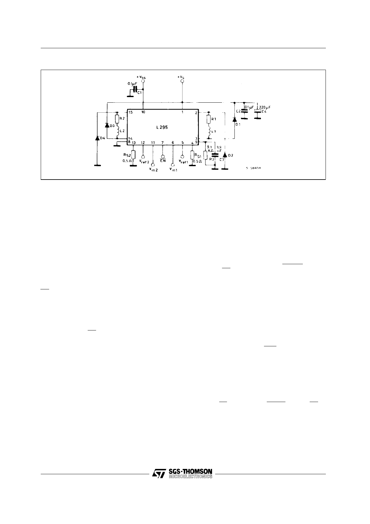
APPLICATION CIRCUIT
Multiwatt 15
ORDER CODE : L295
1/8
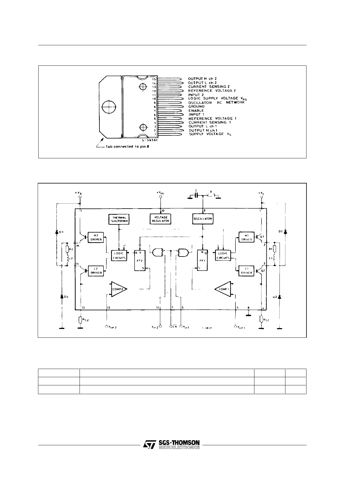
CONNECTION DIAGRAM (top view)
BLOCK DIAGRAM
Symbol
Parameter
Value
Unit
R
th-j-case
Thermal resistance junction-case
max
3
°
C/W
R
th-j-amb
Thermal resistance junction-ambient
max
35
°
C/W
THERMAL DATA
2/8
L295

Symbol
Parameter
Test conditions
Min.
Typ.
Max.
Unit
V
s
Supply Voltage
12
46
V
V
ss
Logic Supply Voltage
4.75
10
V
I
d
Quiescent drain current
(from VSS)
V
S
= 46V; V
i1
= V
i2
= V
EN
= L
4
mA
I
ss
Quiescent drain current
(from VS)
V
SS
= 10 V
46
mA
V
i1
,,V
i2
Input Voltage
Low
-0.3
0.8
V
High
2.2
7
V
EN
Enable Input Voltage
Low
-0.3
0.8
V
High
2.2
7
I
i1
, I
i2
Input Current
V
i1
= V
i2
= L
-100
µ
A
V
i1
= V
i2
= H
10
I
EN
Enable Input Current
V
EN
= L
-100
µ
A
V
EN
= H
10
V
ref1
,
V
ref2
Input Reference Voltage
0.2
2
V
I
ref1
,
I
ref2
m
Input Reference Voltage
-5
µ
A
F
osc
Oscillation Frequency
C = 3.9 nF;
R = 9.1 K
Ω
25
KHz
I
p
Transconductance (each ch.)
V
ref
= 1V
1.9
2
2.1
A/V
V
ref
V
drop
Total output voltage drop
(each channel) (*)
I
o
= 2 A
2.8
3.6
V
V
sens1
V
sens2
External sensing resistors
voltage drop
2
V
(*) V
drop
= V
CEsat
Q1
+ V
CEsat Q2.
ELECTRICAL CHARACTERISTICS (Refer to the application circuit, V
ss
= 5V, V
s
= 36V; T
j
= 25
°
C; L =
Low; H = High; unless otherwise specified)
3/8
L295
APPLICATION CIRCUIT
D2, D4 = 2A High speed diodes
D1, D3 = 1A High speed diodes
R1 = R2 = 2
Ω
L1 = L2 = 5 mH
)
trr
≤
200 ns
FUNCTIONAL DESCRIPTION
The L295 incorporates two indipendent driver
channals with separate inputs and outputs, each
capable of driving an inductive load (see block
diagram).
The device is controlled by three micriprocessor
compatible digital inputs and two analog inputs.
These inputs are:
EN
chip enable (digital input, active low),
enables both channels when in the low
state.
V
in1
, V
in2
channel inputs (digital inputs, active
high), enable each channel inde-
pendently. A channel is actived when
both EN and the appropriate channel
input are active.
V
ref1
, V
ref2
referce
voltages
(analog
inputs),
used
to program the peak load currents.
Peak load current is proportional to V
ref
.
Since the two channels are identical, only channel
one will be described.
The following description applies also the channel
two, replacing FF2 for FF1, V
ref
for V
ref1
etc.
When the channel is avtivated by low level on the
EN input and a high level on the channel input, V
in2
,
the output transistors Q1 and Q2 switch on and
current flows in the load according to the exponen-
tial law:
I
=
V
R1
(
1
−
e
−
R1 t
L1
)
where:
R1 and R2 are the resistance and in-
ductance of the load and V is the volt-
age available on the load (V
s
- V
drop
-
V
sense
).
The current increases until the voltage on the ex-
ternal sensing resistor, R
S1
, reaches the reference
voltage, V
ref1
. This peak current, I
p1
, is given by:
I
p1
=
V
ref1
R
S1
At this point the comparator output, Vomp1, sete
the RS flip-flop, FF1, that turns off the output tran-
sistor, Q1. The load current flowing through D2, Q2,
R
S1
, decreases according to the law:
I
=
(
V
A
R
1
+
I
p1
)
e
−
R1
t
L1
−
V
A
R1
where V
A
= V
CEsat Q2
+ V
sense
+ V
D2
4/8
L295
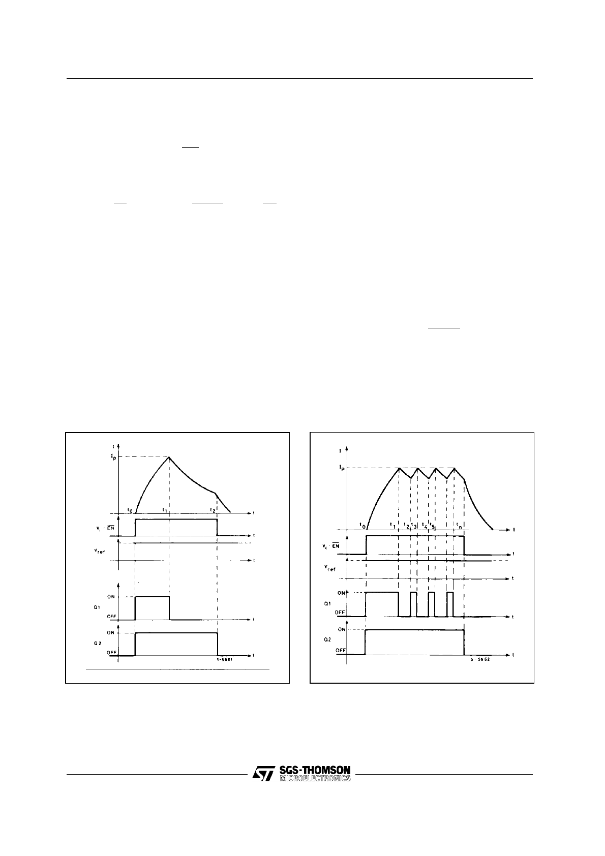
If the oscillator pin (9) is connected to ground the
load current falls to zero as shown in fig. 1.
At this time t
2
the channel 1 is disabled, by taking
the inputs V
in1
low and/or EN high, and the output
transistor Q2 is turned off. The load current flows
through D2 and D1 according to the law:
I
=
(
V
B
R
1
+
I
T2
)
e
−
R1
t
L1
−
V
B
R1
where V
B
= V
S
+ V
D1
+ V
D2
I
T2
= current value at the time t
2
.
Fig. 2 in shows the current waveform obtained with
an RC network connected between pin 9 and
ground. From to t
1
the current increases as in fig.
1. A difference exists at the time t
2
because the
current starts to increase again. At this time a pulse
is produced by the oscillator circuit that resets the
flip.flop, FF1, and switches on the outout transistor,
Q1. The current increases until the drop on the
sensing resistor R
S1
is equal to V
ref1
(t
3
) and the
cycle repeats.
SIGNAL WAVEFORMS
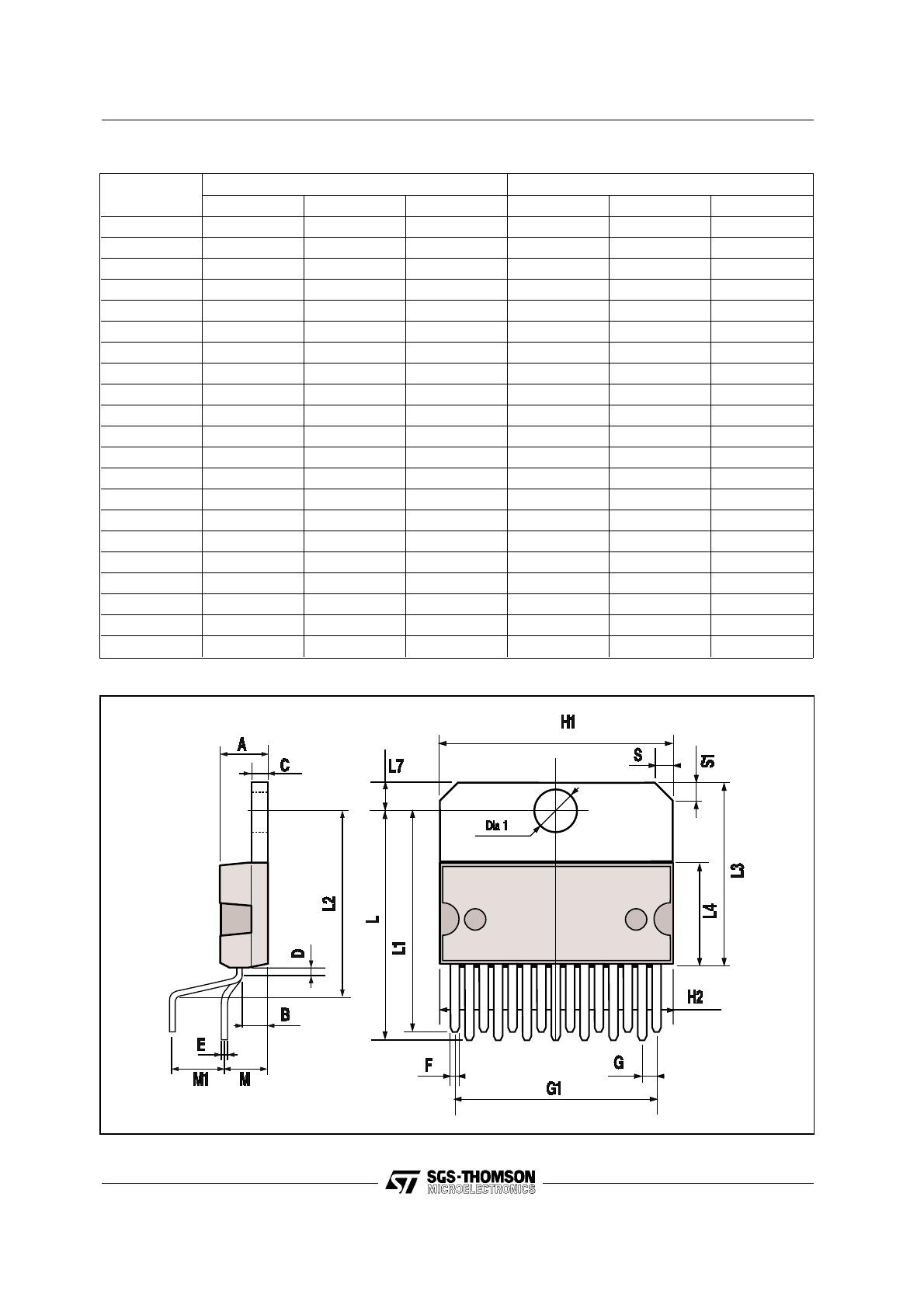
The switching frequency depends on the value R
and C, as shown in fig. 4 and must be chosen in
the range 10 to 30 KHz.
It is possible with external hardware to change the
reference voltage V
ref
in order to obtain a high peak
current I
p
and a lower holding current I
h
(see fig. 3).
The L295 is provided with a thermal protection that
switches off all the output transistors when the
junction temperature exceeds 150
°
C. The pres-
ence of a hysteresis circuit makes the IC work again
aftera fall of the junction temperature of about
20
°
C.
The analog input pins (V
ref1
, V
ref2
) can be left open
or connected to V
ss
; in this case the circuit works
with an internal reference voltage of about 2.5V and
the peak current in the load is fixed only by the value
of R
s
:
I
p
=
2.5
R
S
Figure 1. Load current waveform with pin 9
connected to GND.
Figure 2. Load current waveform with external
R-C network connected between pin 9 and
ground.
5/8
L295
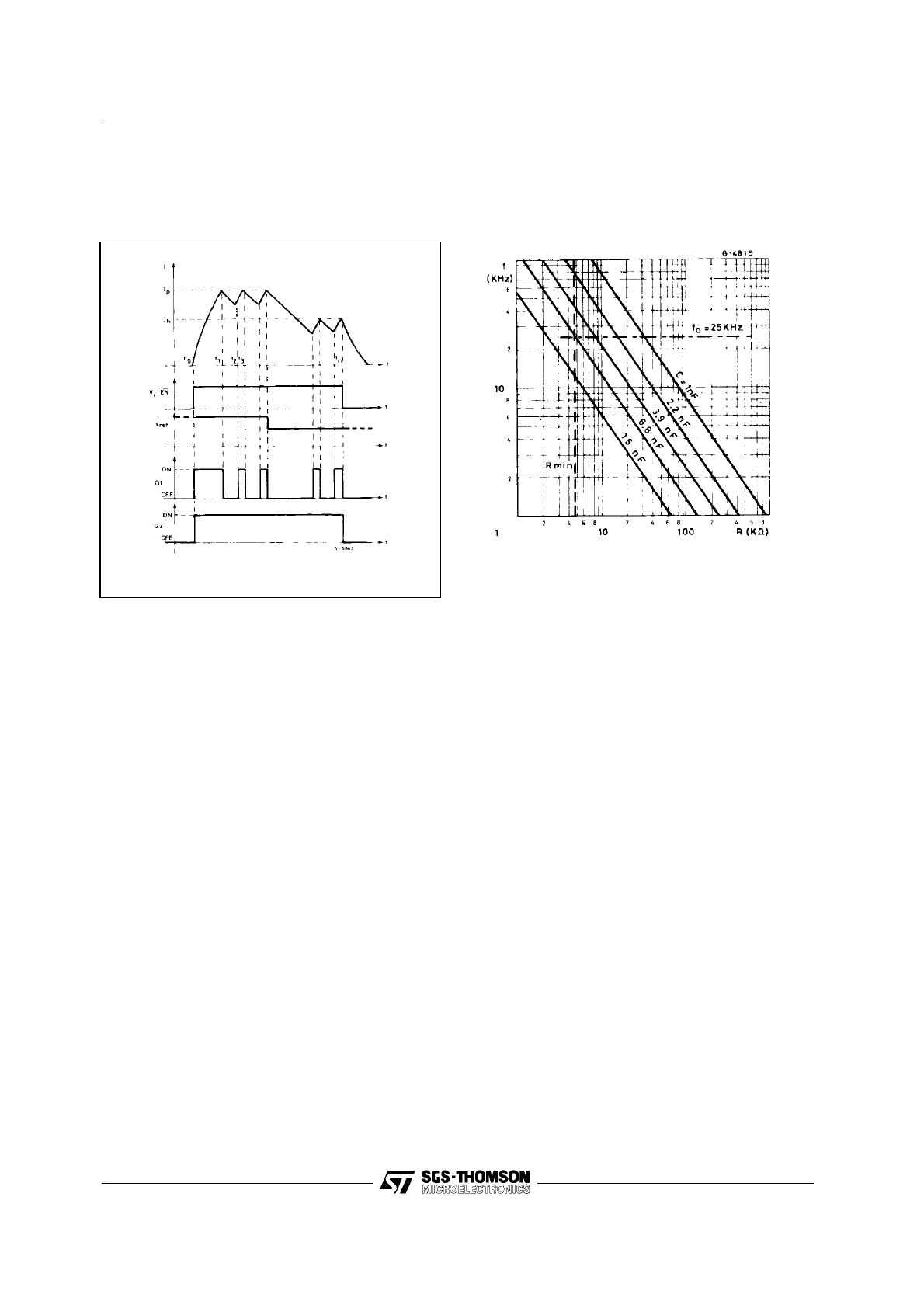
SIGNAL WAVEFORMS (continued)
Figure 3. With V
ref
changed by hardware.
Figure 4. Switching frequency vs. values of R
and C.
6/8
L295
DIM.
mm
inch
MIN.
TYP.
MAX.
MIN.
TYP.
MAX.
A
5
0.197
B
2.65
0.104
C
1.6
0.063
D
1
0.039
E
0.49
0.55
0.019
0.022
F
0.66
0.75
0.026
0.030
G
1.02
1.27
1.52
0.040
0.050
0.060
G1
17.53
17.78
18.03
0.690
0.700
0.710
H1
19.6
0.772
H2
20.2
0.795
L
21.9
22.2
22.5
0.862
0.874
0.886
L1
21.7
22.1
22.5
0.854
0.870
0.886
L2
17.65
18.1
0.695
0.713
L3
17.25
17.5
17.75
0.679
0.689
0.699
L4
10.3
10.7
10.9
0.406
0.421
0.429
L7
2.65
2.9
0.104
0.114
M
4.25
4.55
4.85
0.167
0.179
0.191
M1
4.63
5.08
5.53
0.182
0.200
0.218
S
1.9
2.6
0.075
0.102
S1
1.9
2.6
0.075
0.102
Dia1
3.65
3.85
0.144
0.152
MULTIWATT15 PACKAGE MECHANICAL DATA
7/8
L295

8/8
Information furnished is believed to be accurate and reliable. However, SGS-THOMSON Microelectronics assumes no responsibility for the
consequences of use of such information nor for any infringement of patents or other rights of third parties which may result from its use. No
license is granted by implication or otherwise under any patent or patent rights of SGS-THOMSON Microelectronics. Specifications mentioned
in this publication are subject to change without notice. This publication supersedes and replaces all information previously supplied.
SGS-THOMSON Microelectronics products are not authorized for use as critical components in life support devices or systems without express
written approval of SGS-THOMSON Microelectronics.
© 1994 SGS-THOMSON Microelectronics - All Rights Reserved
SGS-THOMSON Microelectronics GROUP OF COMPANIES
Australia - Brazil - France - Germany - Hong Kong - Italy - Japan - Korea - Malaysia - Malta - Morocco - The Netherlands - Singapore -
Spain - Sweden - Switzerland - Taiwan - Thaliand - United Kingdom - U.S.A.
L295