
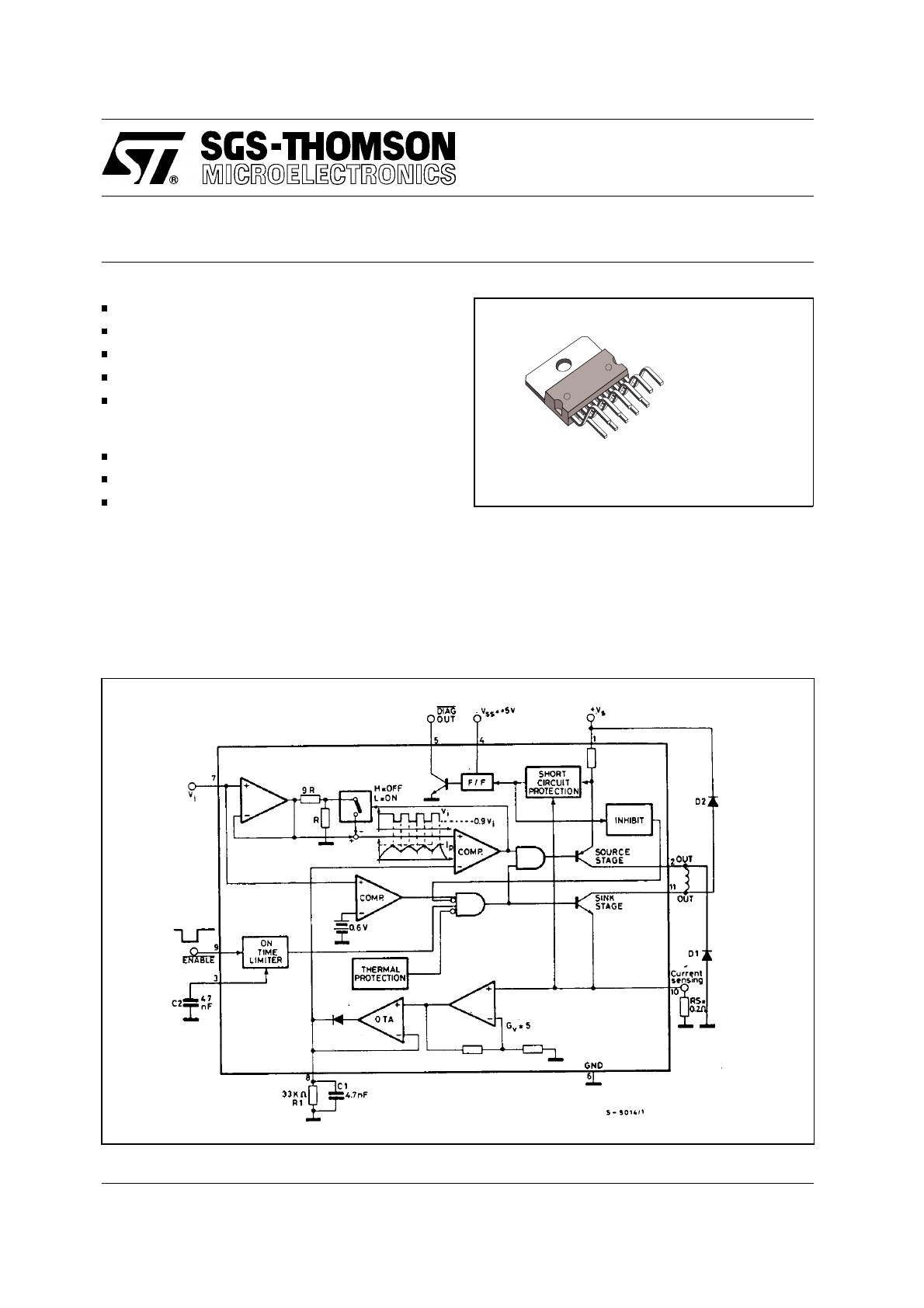
L294
SWITCH-MODE SOLENOID DRIVER
October 1991
HIGH VOLTAGE OPERATION (UP TO 50V)
HIGH OUTPUT CURRENT CAPABILITY (UP TO 4A)
LOW SATURATION VOLTAGE
TTL-COMPATIBLE INPUT
OUTPUT SHORT CIRCUIT PROTECTION (TO
GROUND, TO SUPPLY AND ACROSS THE
LOAD)
THERMAL SHUTDOWN
OVERDRIVING PROTECTION
LATCHED DIAGNOSTIC OUTPUT
DESCRIPTION
The L294 is a monolithic switched mode solenoid
driver designed for fast, high current applications
such as hummer and needle driving in printers and
electronic typewriters. Power dissipation is re-
duced by efficient switchmode operation. An extra
BLOCK DIAGRAM
feature of the L294 is a latched diagnostic output
which indicates when the output is short circuited.
The L294 is supplied in a 11-lead Multiwatt® plas-
tic power package.
Multiwatt 11
ORDER CODE : L294
1/8
2/8
Symbol
Parameter
Value
Unit
V
s
Power Supply Voltage
50
V
V
SS
Logic Supply Voltage
7
V
V
EN
Enable Voltage
7
V
I
p
Peak Output Current (repetitive)
4.5
A
P
tot
Total Power Dissipation (at T
case
= 75
°
C)
25
W
T
stg
, T
j
Storage and Junction Temperature
- 40 to 150
°
C
ABSOLUTE MAXIMUM RATING
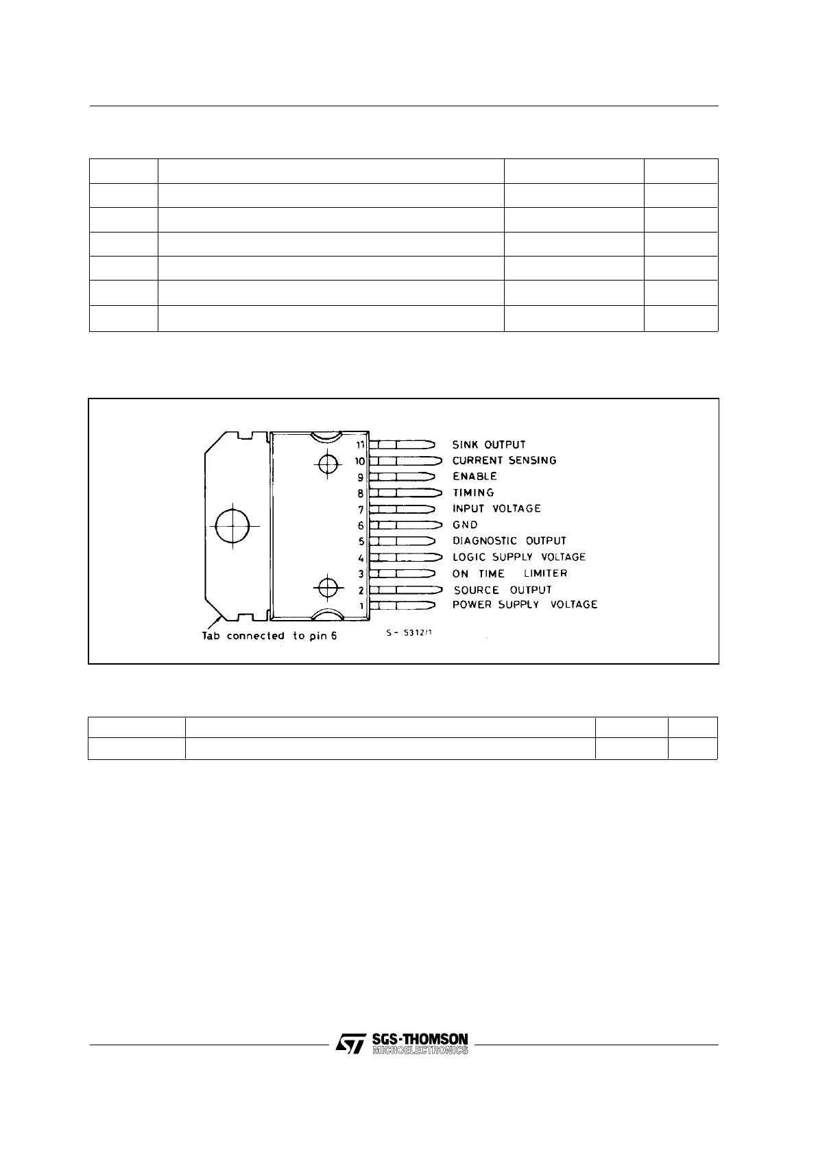
CONNECTION DIAGRAM (top view)
Symbol
Parameter
Value
Unit
Rth-j-case
Thermal resistance junction-case
Max
3
°
C/W
THERMAL DATA
L294

Symbol
Parameter
Test conditions
Min.
Typ.
Max.
Unit
V
s
Power Supply Voltage (pin 1)
Operative Condition
12
46
V
I
d
Quiescent Drain Current (pin 1)
V
ENABLE
= H
20
30
mA
Vi
≥
0.6V; V
ENABLE
= L
70
V
ss
Logic Suply Voltage (pin 4)
4.5
7
V
I
ss
Quiescent Logic Supply
Current
V
DIAG
= L
5
8
mA
DIAG Output at High Impedance
10
100
µ
A
V
i
Input Voltage (pin 7)
Operating Output
0.6
V
Non-operative Output
0.45
I
i
Input Current (pin 7)
V
i
≥
0.6V
-1
µ
A
V
i
≤
0.45V
-3
V
ENABLE
Enable Input Voltage (pin 9)
Low Level
-0.3
0.8
V
High Level
2.4
I
ENABLE
Enable Input Current (pin 9)
V
ENABLE
= L
-100
µ
A
V
ENABLE
= H
100
I
load
/ V
i
Trasconductance
R
S
= 0.2
Ω
V
i
= 1V
0.95
1
1.05
A/V
V
i
= 4V
0.97
1
1.3
V
sat H
Source Output Saturation
Voltage
Ip = 4A
1.7
V
V
sat L
Sink Output Saturation Voltage
Ip = 4A
2
V
V
sat H +
V
satL
Total Saturation Voltage
I
p
= 4A
4.5
V
I
leakage
Output Leakage Current
Rs = 0.2
Ω
; Vi
≤
0.45 V
1
mA
K
On Time Limiter Constant (°)
V
ENABLE
= L
120
V
DIAG
Diagnostic Output Voltage
(pin 5)
I
DIAG
= 10 mA
0.4
V
I
DIAG
Diagnostic Leakage Current
(pin 5)
V
DIAG
= 40V
10
µ
A
V
pin
8
V
pin
10
OP AMP and OTA CD Voltage
Gain (°°)
V
pin
10
= 100 to 800 mV
5
V
SENS
Sensing Voltage (pin 10) (°°°)
0.9
V
ELECTRICAL CHARACTERISTICS (refer to the test circuit, V
s
= 40 V, V
ss
= 5V, T
amb
= 25
°
C, unless
otherwise specified)
(°) After a time interval t
max
= KC
2
, the output stages are disabled.
(°°) See the block diagram.
(°°°) Allowed range of V
SENS
without intervention of the short circuit protection.
3/8
L294

4/8
CIRCUIT OPERATION
The L294 work as a trasconductance amplifier: it
can supply an output current directly proportional
to an input voltage level (V
i
). Fyrthermore, it allows
complete switching control of the output current
waveform (see fig. 1).
The following explanation refers to the Block Dia-
gram, to fig. 1 and to the typical application circuit
of fig. 2.
The t
on
time is fixed by the width of the Enable input
signal (TTL compatible): it is active low and enables
the output stages "source" and "sink". At the end of
t
on
, the load current I
load
recirculates through D1
and D2, allowing fast current turn-off.
The rise time t
r
, depends on the load charac-
teristics, on V
i
and on the supply voltage value (V
s
,
pin 1). During the t
on
time, I
load
is converter into a
voltage signal by means of the external sensing
resistance R
s
connected to pin 10. This signal,
amplified by the op amp and converted by the
transconductance amplifier OTA, charges the ex-
ternal RC network at pin 8 (R1, C1). The voltage at
this pin is sensed by the inverting input of a com-
parator. The voltage on the non-inverting input of
this one is fixed by the external voltage V
i
(pin 7).
After t
r
, the comparator switches and the output
stage "source" is switched off. The comaprator
output is confirmed by the voltage on the non-in-
verting input, which decreases of a costant fraction
of V
i
(1/10), allowing hysteresis operation. The
current in the load now flow through D1.
Two Cases are possible: the time constant of the
recirculation phase is higher than R1.C1; the time
constant is lower than R1.C1. In the first case, the
voltage sensed in the non-inverting input of the
comparator is just the value proportional to I
load
. In
the second case, when the current decreases too
quickly, the comparator senses the voltage signal
stored in the R1 C1 network.
In the first case t
1
depends on the load charac-
teristics, while in the second case it depends only
on the value of R1. C1.
In the other words, R1. C1 fixes the minimum value
of t
1
)t
1
≥
1/10 R1.C1. Note that C1 should be
chosen in the range 2.7 to 10 nF for stability rea-
sons of the OTA).
After t
1
, the comparator switches again: the output
is confirmed by the voltage on the non-inverting
input, which reaches V
i
again (hysteresis).
Now the cycle starts again: t
2
, t
4
and t
6
have the
same characteristics as t
r
, while t
3
and t
5
are similar
to t
1
. The peak current I
p
depends on V
i
as shown
in the typical transfer function of fig.3.
It can be seen that for V
i
lower than 450 mV the
device is not operating.
For V
i
greater than 600 mV, the L294 has a tran-
sconductance of 1A/V with R
s
= 0.2
Ω
. For V
i
in-
cluded between 450 and 600 mV, the operation is
not guaranteed.
The order parts of the device have protection and
diagnostic functions. At pin 3 is connected an ex-
ternal capacitor C2, charged at costant current
when the Enable is low.
After a time interval equal to K C2 (K is defined in
the table of Electrical Characteristics and has the
dimensions of ohms) the output stages are
switched off independently by the Input signal.
This avoids the load being driven in conduction for
an excessive period of time (overdriving protec-
tion). The action of this protection is shown in fig.
1b. Note that the voltage ramp at pin 3 starts
whenever the Enable signal becomes active (low
state), regardless of the Input signal. To reset pin 3
and to restore the normal conditions, pin 9 must
return high.
This protection can be disabled by grounding pin 3.
The thermal protection included in the L294 has a
hysteresis.
It switches off the output stages whenever the
junction temperature increases too much. After a
fall of about 20
°
C, the circuit starts again.
Finally, the device is protected against any type of
short circuit at the outputs: to ground, to supply and
across the load.
When the source stage current is higher than 5A
and/or when the pin 10 voltage is higher then 1V
(i.e. for a sink current greater than 1V/R
s
) the output
stages are switched off and the device is inhibited.
This condition is indicated at the open-collector
output DIAG (pin 5); the internal flip-flop F/F
changes and forces the output transistor into satu-
ration. The F/F must be supplied independently
through V
ss
(pin 4). The DIAG signal is reset and
the output stages are still operative by switching the
device on again. After that, two cases are possible:
the reason for the "bad operation" is still present
and the protection acts again; the reason has been
removed and the device starts to work properly.
L294
Figure 1. Output Current Waveforms.
Figure 2. Test and Typical Application Circuit.
Figure 3. Peak Output Current vs. Input
Voltage.
Figure 4. Output Saturation Voltage vs.
Peak Output Current.
D1 : 3A fast diode
200 ns
trr
≤
}
5/8
L294
6/8
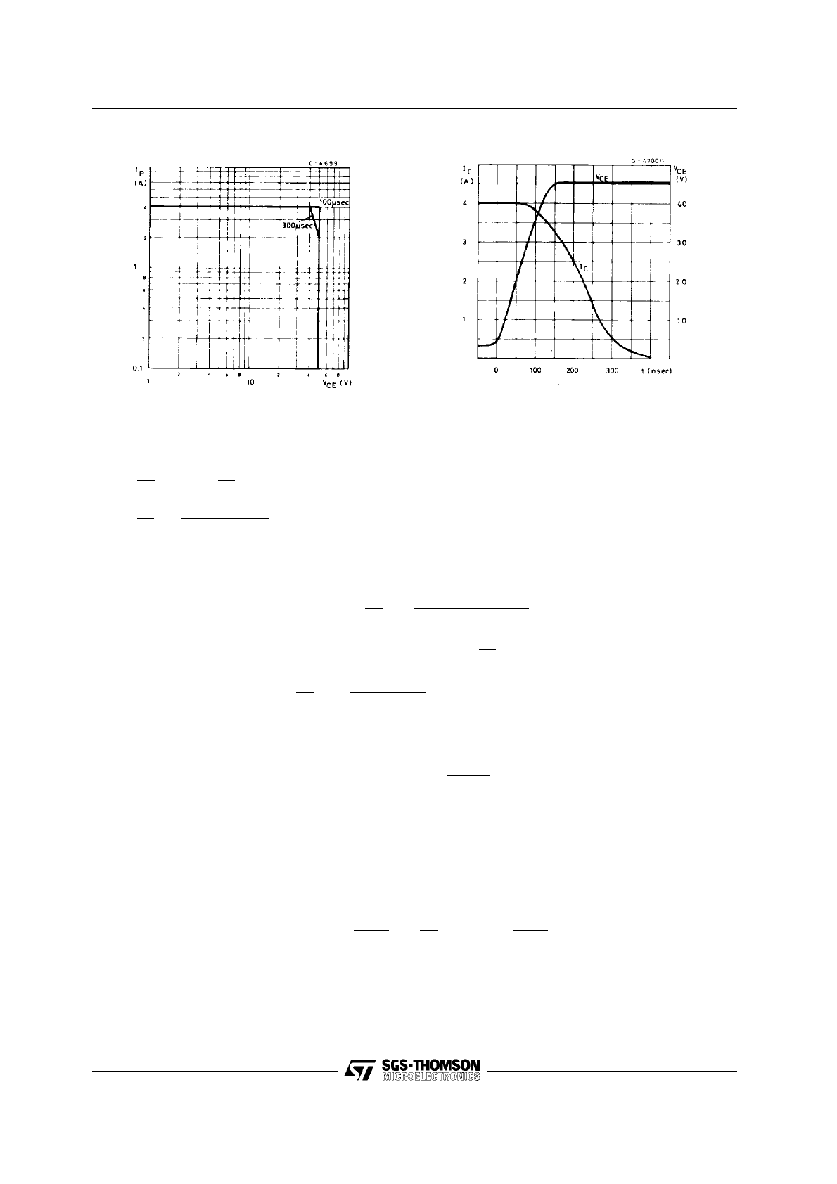
Figure 5. Safe Operating Areas.
Figure 6. Turn-off Phase.
CALCULATION OF THE SWITCHING TIMES
Referring to the block diagram and to the waveforms of fig. 1, it is possible to calculate the switching times
by means of the following relationships.
t
r
=
−
L
R
L
In
(
1
−
R
L
V
1
•
I
p
)
where : V1 = V
s
- V
sat L
- V
sat H
_ V
R sens
t
f
=
−
L
R
L
In
V2
V2
+
R
L
•
I
o
where : V2 = V
s
+ V
D1
+ V
D2
I
K
≤
I
o
≤
I
p
I
o
is the value of the load current at the end of t
on
.
t
1
= t
3
= t
5
= ...
a
)
−
L
R
L
In
0.9 I
p
•
R
L
+
V3
I
p
R
L
+
V3
where
V3 = V
sat L
+ V
R sens
+ V
D1
b
)
−
R1 C1 In 0.9
≅
1
10
R1
C1
t
2
= t
4
= t
6
= ...
=
−
L
R
L
In
(
V1
−
I
p
R
L
V1
−
I
K
R
L
)
Note that the time interval t
1
= t
3
= t
5
= ... takes the longer value between case a) and case b). The switching
frequency is always :
f
switching
=
1
t
1
+
t
2
In the case a) the main regulation loop is always closed and it forces :
I
K
= (0.9
±
S) I
p
where : S = 3 % @ Vi = 1 V
S = 1.5 % @ Vi = 4 V
In the case b), the same loop is open in the recirculation phase and I
K
, which is always lower than 0.9 I
p
,
is obtained by means of the following relationship.
I
K
=
I
p
e
−
t
1
R
L
L
−
V3
R
L
(
1
−
e
−
t
1
R
L
L
)
With the typical application circuit, in the conditions Vs = 40V, Ip = 4A, the following switching times result:
t
r
= 255
µ
s t
f
= 174
µ
s @ I
o
= I
p
t1 =
a) 70
µ
s
b) 16
µ
s t2 = 29
µ
s f = 10.2 KHz
=
L294
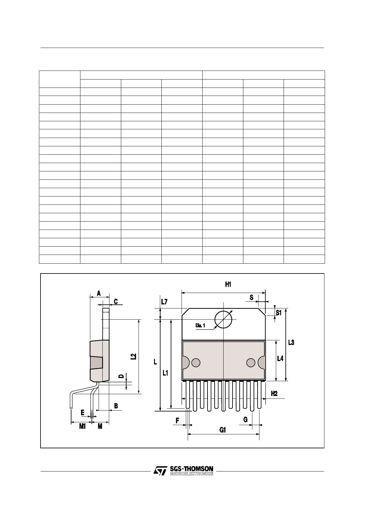
DIM.
mm
inch
MIN.
TYP.
MAX.
MIN.
TYP.
MAX.
A
5
0.197
B
2.65
0.104
C
1.6
0.063
D
1
0.039
E
0.49
0.55
0.019
0.022
F
0.88
0.95
0.035
0.037
G
1.57
1.7
1.83
0.062
0.067
0.072
G1
16.87
17
17.13
0.664
0.669
0.674
H1
19.6
0.772
H2
20.2
0.795
L
21.5
22.3
0.846
0.878
L1
21.4
22.2
0.843
0.874
L2
17.4
18.1
0.685
0.713
L3
17.25
17.5
17.75
0.679
0.689
0.699
L4
10.3
10.7
10.9
0.406
0.421
0.429
L7
2.65
2.9
0.104
0.114
M
4.1
4.3
4.5
0.161
0.169
0.177
M1
4.88
5.08
5.3
0.192
0.200
0.209
S
1.9
2.6
0.075
0.102
S1
1.9
2.6
0.075
0.102
Dia1
3.65
3.85
0.144
0.152
MULTIWATT11 PACKAGE MECHANICAL DATA
7/8
L294

8/8
Information furnished is believed to be accurate and reliable. However, SGS-THOMSON Microelectronics assumes no responsibility for the
consequences of use of such information nor for any infringement of patents or other rights of third parties which may result from its use. No
license is granted by implication or otherwise under any patent or patent rights of SGS-THOMSON Microelectronics. Specifications mentioned
in this publication are subject to change without notice. This publication supersedes and replaces all information previously supplied.
SGS-THOMSON Microelectronics products are not authorized for use as critical components in life support devices or systems without express
written approval of SGS-THOMSON Microelectronics.
© 1994 SGS-THOMSON Microelectronics - All Rights Reserved
SGS-THOMSON Microelectronics GROUP OF COMPANIES
Australia - Brazil - France - Germany - Hong Kong - Italy - Japan - Korea - Malaysia - Malta - Morocco - The Netherlands - Singapore -
Spain - Sweden - Switzerland - Taiwan - Thaliand - United Kingdom - U.S.A.
L294