
L293D
L293DD
PUSH-PULL FOUR CHANNEL DRIVER WITH DIODES
600mA OUTPUT CURRENT CAPABILITY
PER CHANNEL
1.2A PEAK OUTPUT CURRENT (non repeti-
tive) PER CHANNEL
ENABLE FACILITY
OVERTEMPERATURE PROTECTION
LOGICAL ”0” INPUT VOLTAGE UP TO 1.5 V
(HIGH NOISE IMMUNITY)
INTERNAL CLAMP DIODES
DESCRIPTION
The Device is a monolithic integrated high volt-
age, high current four channel driver designed to
accept standard DTL or TTL logic levels and drive
inductive loads (such as relays solenoides, DC
and stepping motors) and switching power tran-
sistors.
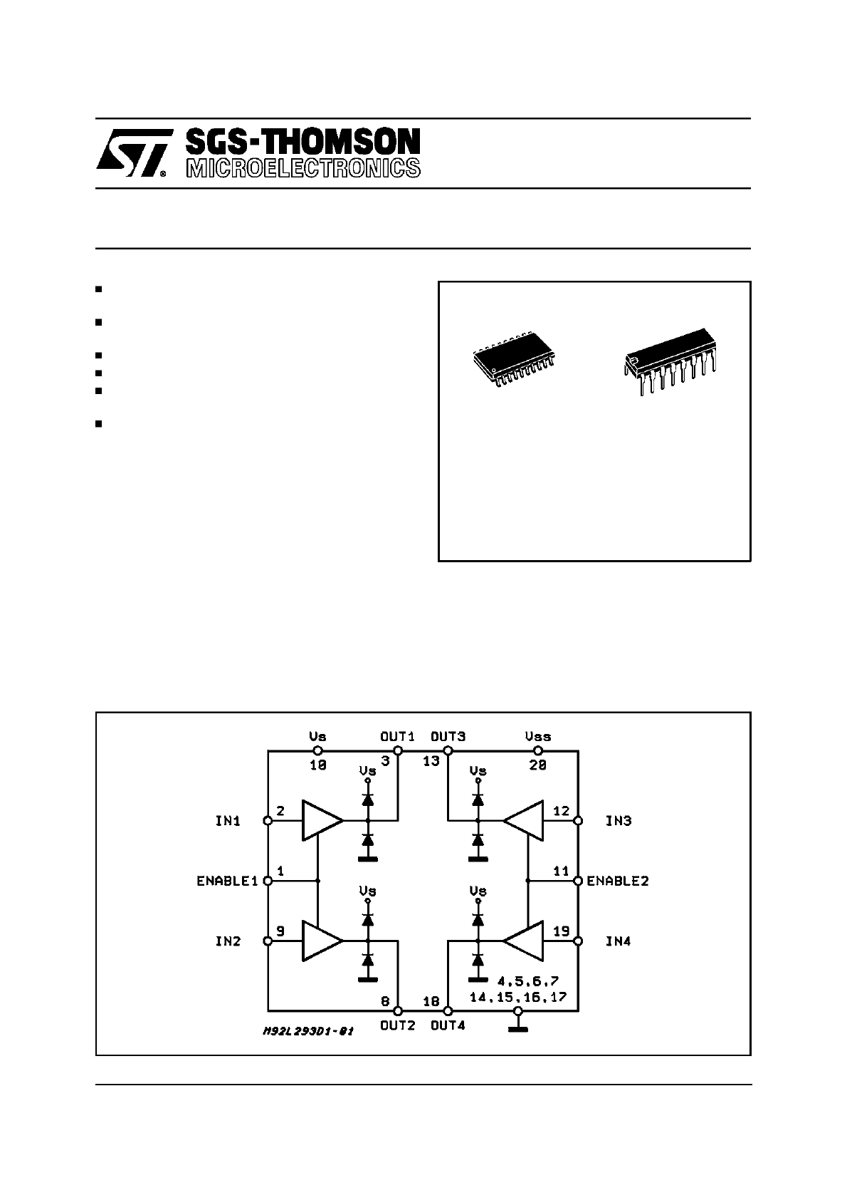
To simplify use as two bridges each pair of chan-
nels is equipped with an enable input. A separate
supply input is provided for the logic, allowing op-
eration at a lower voltage and internal clamp di-
odes are included.
This device is suitable for use in switching appli-
cations at frequencies up to 5 kHz.
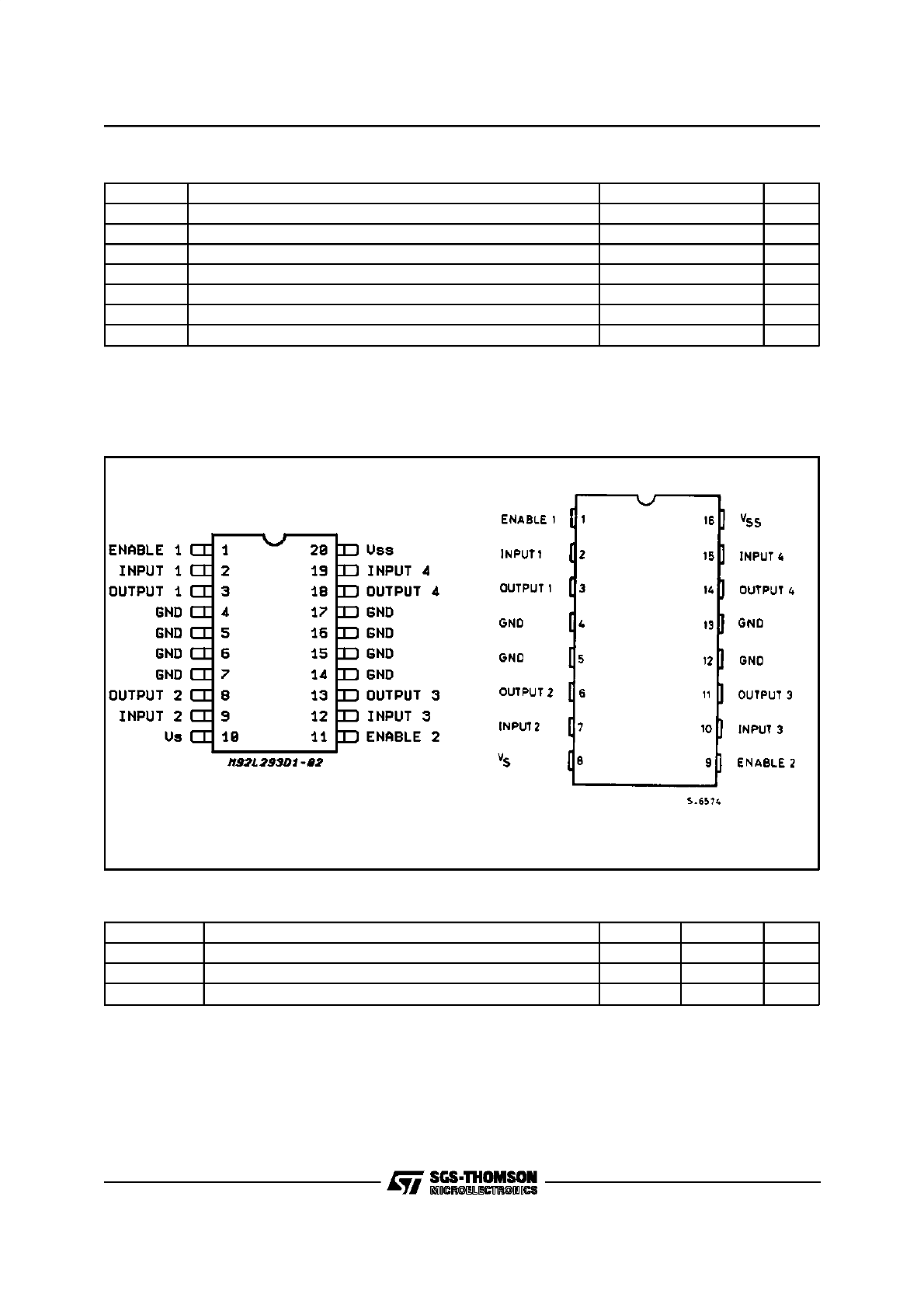
The L293D is assembled in a 16 lead plastic
packaage which has 4 center pins connected to-
gether and used for heatsinking
The L293DD is assembled in a 20 lead surface
mount which has 8 center pins connected to-
gether and used for heatsinking.
June 1996
BLOCK DIAGRAM
SO(12+4+4)
Powerdip (12+2+2)
ORDERING NUMBERS:
L293DD
L293D
1/7
ABSOLUTE MAXIMUM RATINGS
Symbol
Parameter
Value
Unit
V
S
Supply Voltage
36
V
V
SS
Logic Supply Voltage
36
V
V
i
Input Voltage
7
V
V
en
Enable Voltage
7
V
I
o
Peak Output Current (100
µ
s non repetitive)
1.2
A
P
tot
Total Power Dissipation at T
pins
= 90
°
C
4
W
T
stg
, T
j
Storage and Junction Temperature
– 40 to 150
°
C
THERMAL DATA
Symbol
Decription
DIP
SO
Unit
R
th j-pins
Thermal Resistance Junction-pins
max.
–
14
°
C/W
R
th j-amb
Thermal Resistance junction-ambient
max.
80
50 (*)
°
C/W
R
th j-case
Thermal Resistance Junction-case
max.
14
–
(*) With 6sq. cm on board heatsink.
PIN CONNECTIONS (Top view)
SO(12+4+4)
Powerdip(12+2+2)
L293D - L293DD
2/7

ELECTRICAL CHARACTERISTICS (for each channel, V
S
= 24 V, V
SS
= 5 V, T
amb
= 25
°
C, unless
otherwise specified)
Symbol
Parameter
Test Conditions
Min.
Typ.
Max.
Unit
V
S
Supply Voltage (pin 10)
V
SS
36
V
V
SS
Logic Supply Voltage (pin 20)
4.5
36
V
I
S
Total Quiescent Supply Current
(pin 10)
V
i
= L ; I
O
= 0 ; V
en
= H
2
6
mA
V
i
= H ; I
O
= 0 ; V
en
= H
16
24
mA
V
en
= L
4
mA
I
SS
Total Quiescent Logic Supply
Current (pin 20)
V
i
= L ; I
O
= 0 ; V
en
= H
44
60
mA
V
i
= H ; I
O
= 0 ; V
en
= H
16
22
mA
V
en
= L
16
24
mA
V
IL
Input Low Voltage (pin 2, 9, 12,
19)
– 0.3
1.5
V
V
IH
Input High Voltage (pin 2, 9,
12, 19)
V
SS
≤
7 V
2.3
V
SS
V
V
SS
> 7 V
2.3
7
V
I
IL
Low Voltage Input Current (pin
2, 9, 12, 19)
V
IL
= 1.5 V
– 10
µ
A
I
IH
High Voltage Input Current (pin
2, 9, 12, 19)
2.3 V
≤
V
IH
≤
V
SS
– 0.6 V
30
100
µ
A
V
en L
Enable Low Voltage
(pin 1, 11)
– 0.3
1.5
V
V
en H
Enable High Voltage
(pin 1, 11)
V
SS
≤
7 V
2.3
V
SS
V
V
SS
> 7 V
2.3
7
V
I
en L
Low Voltage Enable Current
(pin 1, 11)
V
en L
= 1.5 V
– 30
– 100
µ
A
I
en H
High Voltage Enable Current
(pin 1, 11)
2.3 V
≤
V
en H
≤
V
SS
– 0.6 V
±
10
µ
A
V
CE(sat)H
Source Output Saturation
Voltage (pins 3, 8, 13, 18)
I
O
= – 0.6 A
1.4
1.8
V
V
CE(sat)L
Sink Output Saturation Voltage
(pins 3, 8, 13, 18)
I
O
= + 0.6 A
1.2
1.8
V
V
F
Clamp Diode Forward Voltage
I
O
= 600nA
1.3
V
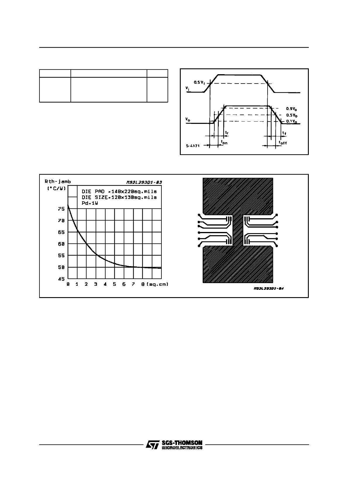
t
r
Rise Time (*)
0.1 to 0.9 V
O
250
ns
t
f
Fall Time (*)
0.9 to 0.1 V
O
250
ns
t
on
Turn-on Delay (*)
0.5 V
i
to 0.5 V
O
750
ns
t
off
Turn-off Delay (*)
0.5 V
i
to 0.5 V
O
200
ns
(*) See fig. 1.
L293D - L293DD
3/7
TRUTH TABLE (one channel)
Inpu t
Enable (*)
Output
H
L
H
L
H
H
L
L
H
L
Z
Z
Z = High output impedance
(*) Relative to the considered channel
Figure 1: Switching Times
Figure 2: Junction to ambient thermal resistance vs. area on board heatsink (SO12+4+4 package)
L293D - L293DD
4/7
POWERDIP16 PACKAGE MECHANICAL DATA
DIM.
mm
inch
MIN.
TYP.
MAX.
MIN.
TYP.
MAX.
a1
0.51
0.020
B
0.85
1.40
0.033
0.055
b
0.50
0.020
b1
0.38
0.50
0.015
0.020
D
20.0
0.787
E
8.80
0.346
e
2.54
0.100
e3
17.78
0.700
F
7.10
0.280
I
5.10
0.201
L
3.30
0.130
Z
1.27
0.050
L293D - L293DD
5/7
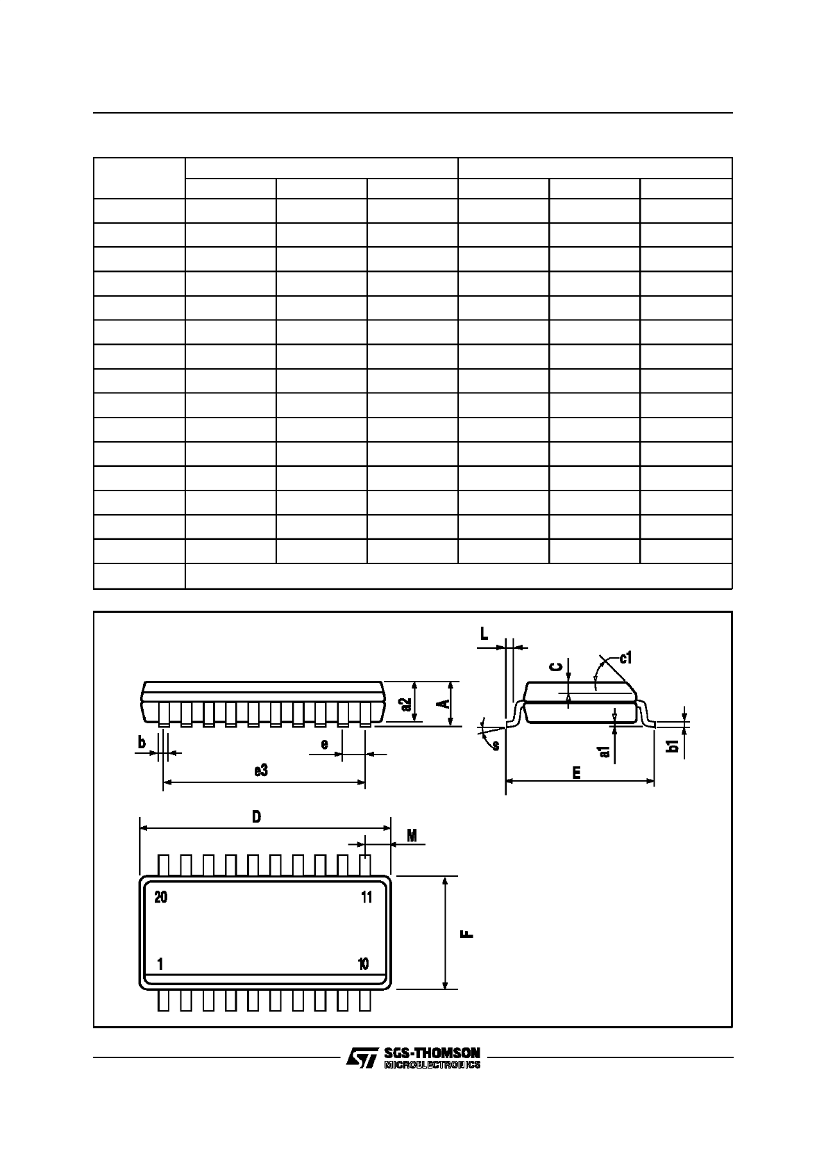
SO20 PACKAGE MECHANICAL DATA
DIM.
mm
inch
MIN.
TYP.
MAX.
MIN.
TYP.
MAX.
A
2.65
0.104
a1
0.1
0.2
0.004
0.008
a2
2.45
0.096
b
0.35
0.49
0.014
0.019
b1
0.23
0.32
0.009
0.013
C
0.5
0.020
c1
45
1.772
D
1
12.6
0.039
0.496
E
10
10.65
0.394
0.419
e
1.27
0.050
e3
11.43
0.450
F
1
7.4
0.039
0.291
G
8.8
9.15
0.346
0.360
L
0.5
1.27
0.020
0.050
M
0.75
0.030
S
8
°
(max.)
L293D - L293DD
6/7

Information furnished is believed to be accurate and reliable. However, SGS-THOMSON Microelectronics assumes no responsibility for the
consequences of use of such information nor for any infringement of patents or other rights of third parties which may result from its use. No
license is granted by implication or otherwise under any patent or patent rights of SGS-THOMSON Microelectronics. Specification mentioned
in this publication are subject to change without notice. This publication supersedes and replaces all information previously supplied.
SGS-THOMSON Microelectronics products are not authorized for use as criticalcomponents in life support devices or systems without express
written approval of SGS-THOMSON Microelectronics.
1996 SGS-THOMSON Microelectronics – Printed in Italy – All Rights Reserved
SGS-THOMSON Microelectronics GROUP OF COMPANIES
Australia - Brazil - Canada - China - France - Germany - Hong Kong - Italy - Japan - Korea - Malaysia - Malta - Morocco - The Netherlands -
Singapore - Spain - Sweden - Switzerland - Taiwan - Thailand - United Kingdom - U.S.A.
L293D - L293DD
7/7