
L293C
April 1993
H-BRIDGE DRIVER
PRELI MINARY DATA
PUSH-PULL FOUR CHANNEL/DUAL
.
600 mA OUTPUT CURRENT CAPABILITY PER
CHANNEL
.
1.2 A PEAK OUTPUT CURRENT (non repetitive)
PER CHANNEL
.
ENABLE FACILITY
.
OVERTEMPERATURE PROTECTION
.
LOGICAL ”0” INPUT VOLTAGE UP TO 1.5 V
(high noise immunity)
.
SEPARATE HIGH VOLTAGE POWER SUPPLY
(up to 44 V)
DESCRIPTION
The L293C is a monolithic high voltage, high current
integrated circuit four channel driver in a 20 pin DIP.
It is designed to accept standard TTL or DTL input
logic levels and drive inductive loads (such as re-
lays, solenoids, DC and stepping motors) and
switching power transistors.
The device may easily be used as a dual H-bridge
driver : separate chip enable and highvoltage power
supply pins are provided for each H-bridge. In addi-
tion, a separate power supply is provided for the
logic section of the device.
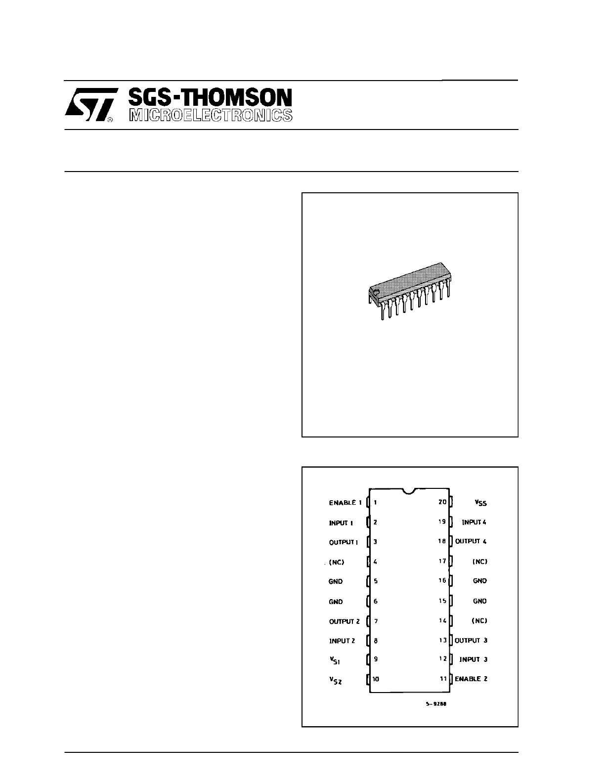
The L293C is assembled in a 20 lead plastic pack-
age which has 4 centerpins connected togetherand
used for heatsinking.
POWERDIP (16 + 2 + 2)
ORDERING NUMBER : L293C
PIN CONNECTION
1/5
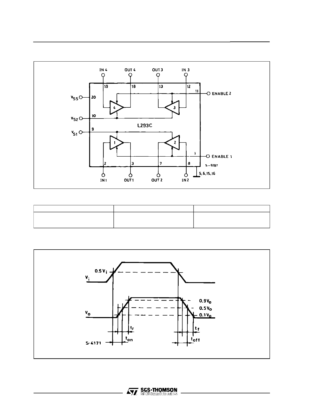
BLOCK DIAGRAM
TRUTH TABLE
Input
Enable
Output
H
L
X
H
H
L
H
L
Z
Z = High output impedance
SWITCHING TIMES
L293C
2/5
ABSOLUTE MAXIMUM RATINGS
Symbol
Parameter
Value
Unit
V
S
Supply Voltage
50
V
V
SS
Logic Supply Voltage
7
V
V
i
Input Voltage
7
V
V
EN
Enable Voltage
7
V
I
out
Peak Output Current (non–repetitive t = 5 ms)
1.2
A
P
tot
Total Power Dissipation at T
ground–pins
= 80
o
C
5
W
T
stg
, T
j
Storage and Junction Temperature
–40 to 150
o
C
THERMAL DATA
Symbol
Parameter
Value
Unit
R
th j-case
Thermal Resistance Junction-case
Max.
14
o
C/
Ω
R
th j-amb
Thermal Resistance Junction-ambient
Max.
80
o
C/
Ω
ELECTRICAL CHARACTERISTICS
(for each channel, V
S
= 24 V, V
SS
= 5 V, T
amb
= 25
o
C, unless otherwise specified)
Symbol
Parameter
Test Conditions
Min.
Typ.
Max.
Unit
V
S
Supply Voltage (pin 9, 10)
V
SS
44
V
V
SS
Logic Supply Voltage (pin 20)
4.5
7
V
I
S
Total Quiescent Supply Current (pin 9, 10)
V
i
= L
I
O
= 0
V
EN
= H
V
i
= H I
O
= 0
V
EN
= H
V
EN
= L
2
16
6
24
4
mA
I
SS
Total Quiescent Logic Supply Current (pin 20)
V
i
= L
I
O
= 0
V
EN
= H
V
i
= H I
O
= 0
V
EN
= H
V
EN
= L
44
16
16
60
22
24
mA
V
IL
Input Low Voltage (pin 2, 8, 12, 19)
-0.3
1.5
V
V
IH
Input High Voltage (pin 2, 8, 12, 19)
2.3
V
SS
V
I
IL
Low Voltage Input Current (pin 2, 8, 12, 19)
V
i
= 1.5 V
-10
µ
A
I
IH
High Voltage Input Current (pin 2, 8, 12, 19)
2.3 V
≤
V
i
≤
V
SS
– 0.6 V
30
100
µ
A
V
EN L
Enable Low Voltage (pin 1, 11)
-0.3
1.5
V
V
EN H
Enable High Voltage (pin 1, 11)
2.3
V
SS
V
I
EN L
Low Voltage Enable Current (pin 1, 11)
V
EN L
= 1.5 V
-30
-100
µ
A
I
EN H
High Voltage Enable Current (pin 1, 11)
2.3 V
≤
V
EN H
≤
V
SS
– 0.6
±
10
µ
A
V
CE(sat)H
Source Output Saturation Voltage
(pins 3, 7, 13, 18)
I
O
= – 0.6 A
1.4
1.8
V
V
CE(sat)L
Sink Output Saturation Voltage
(pins 3, 7, 13, 18)
I
O
= + 0.6 A
1.2
1.8
V
t
r
Rise Time (*)
0.1 to 0.9 V
O
250
ns
t
f
Fall Time (*)
0.9 to 0.1 V
O
250
ns
t
on
Turn-on Delay (*)
0.5 V
i
to 0.5 V
O
750
ns
t
off
Turn-off Delay (*)
0.5 V
i
to 0.5 V
O
200
ns
(*) See switching times diagram
L293C
3/5
20
11
1
10
I
a1
L
B
e
D
Z
b
Z
e3
F
b1
E
PMDIP20W.EPS
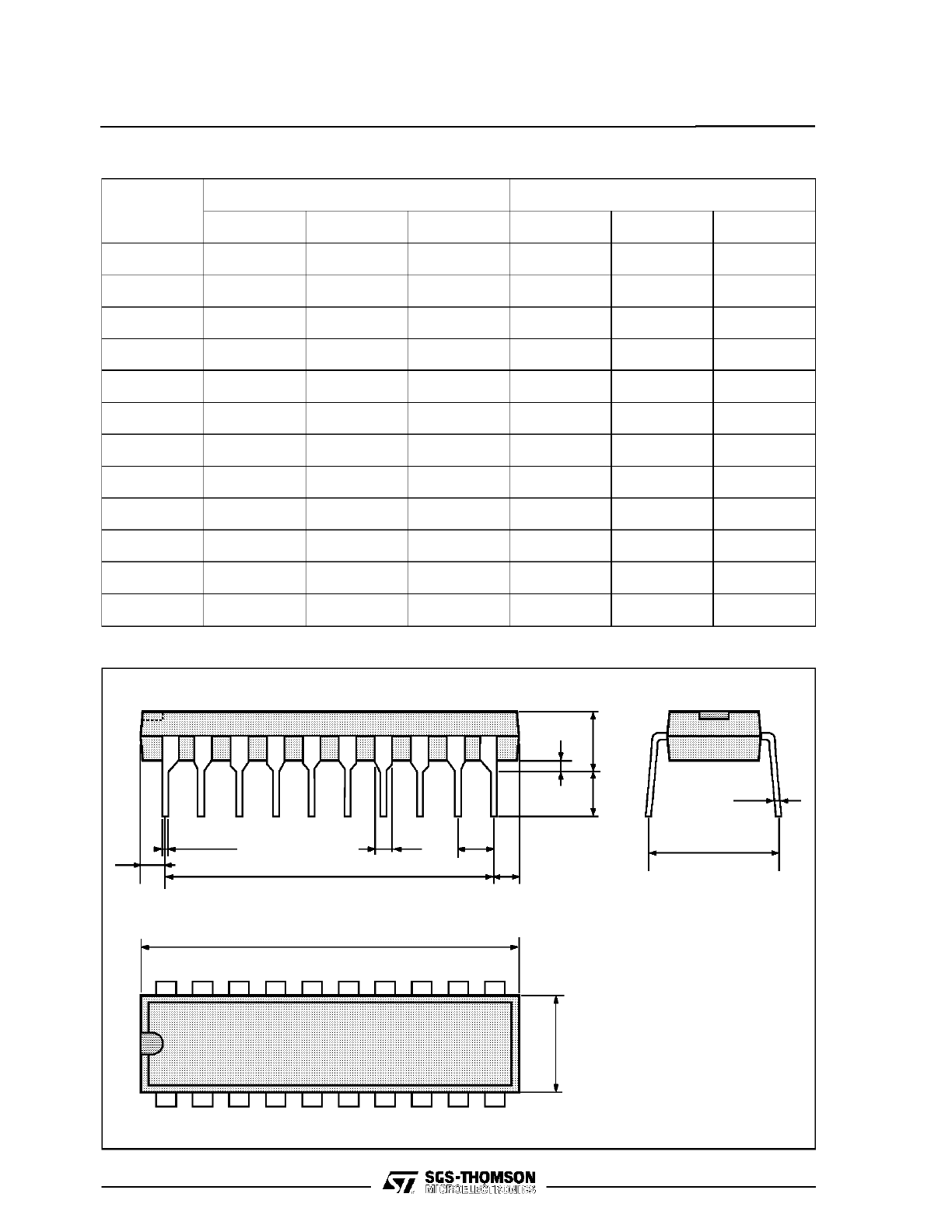
POWERDIP (16 + 2 +2) PACKAGE MECHANICAL DATA
Dimensions
Millimeters
Inches
Min.
Typ.
Max.
Min.
Typ.
Max.
a1
0.51
0.020
B
0.85
1.4
0.033
0.055
b
0.5
0.020
b1
0.38
0.5
0.015
0.020
D
24.8
0.976
E
8.8
0.346
e
2.54
0.100
e3
22.86
0.900
F
7.1
0.280
i
5.1
0.201
L
3.3
0.130
Z
1.27
0.050
DIP20PW.TBL
L293C
4/5

Information furnished is believed to be accurate and reliable. However, SGS-THOMSON Microelectronics assumes no responsibility for
the consequences of use of such information nor for any infringement of patents or other rights of third parties which may result from its
use. No license is granted by implication or otherwise under any patent or patent rights of SGS-THOMSON Microelectronics. Specifica-
tions mentioned in this publication are subject to change without notice. This publication supersedes and replaces all information pre-
viously supplied. SGS-THOMSON Microelectronics products are not authorized for use as critical components in life support devices or
systems without express written approval of SGS-THOMSON Microelectronics.
1994 SGS-THOM SON Microelectronics - All Rights Reserved
SGS-THOM SON Microelectronics GROUP OF COMPANIES
Australia - Brazil - France - Germany - Hong Kong - Italy - Japan - Korea - Malaysia - Malta - Morocco - The Nether-
lands - Singapore - Spain - Sweden - Switzerland - Taiwan - Thaliand - United Kingdom - U.S.A.
L293C
5/5