
1N581x
July 1999 - Ed: 2A
LOW DROP POWER SCHOTTKY RECTIFIER
®
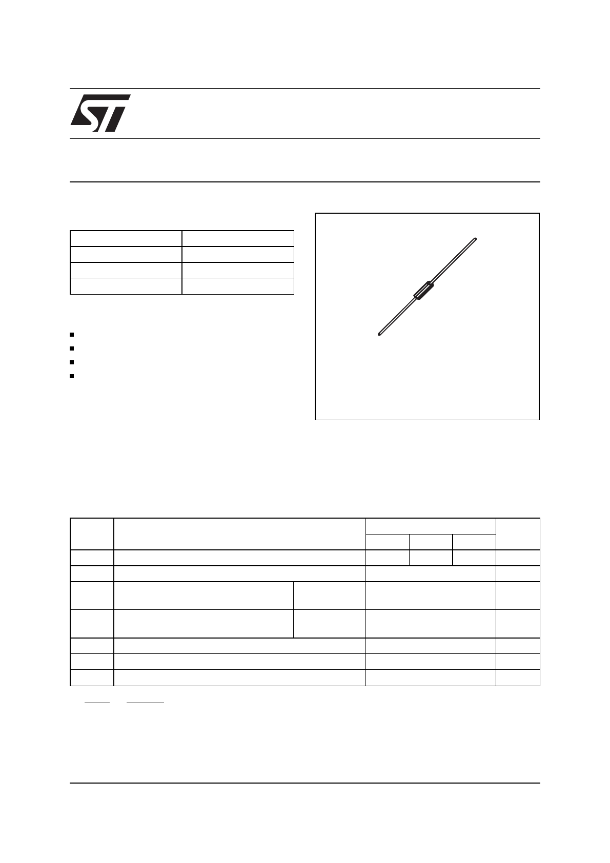
Axial Power Schottky rectifier suited for Switch
Mode Power Supplies and high frequency DC to
DC converters. Packaged in DO41 these devices
are intended for use in low voltage, high frequency
inverters, free wheeling, polarity protection and
small battery chargers.
DESCRIPTION
VERY SMALL CONDUCTION LOSSES
NEGLIGIBLE SWITCHING LOSSES
EXTREMELY FAST SWITCHING
LOW FORWARD VOLTAGE DROP
FEATURES AND BENEFITS
Symbol
Parameter
Value
Unit
1N5817 1N5818 1N5819
V
RRM
Repetitive peak reverse voltage
20
30
40
V
I
F(RMS)
RMS forward current
10
A
I
F(AV)
Average forward current
T
L
= 125
°
C
δ
= 0.5
1
A
I
FSM
Surge non repetitive forward current
tp = 10 ms
Sinusoidal
25
A
T
stg
Storage temperature range
- 65 to + 150
°
C
Tj
Maximum operating junction temperature *
150
°C
dV/dt
Critical rate of rise of reverse voltage
10000
V/
µ
s
ABSOLUTE RATINGS (limiting values)
I
F(AV)
1 A
V
RRM
40 V
T
j
150°C
V
F
(max)
0.45 V
MAIN PRODUCTS CHARACTERISTICS
DO41
* :
dPtot
dTj
<
1
Rth
(
j
−
a
)
thermal runaway condition for a diode on its own heatsink
1/5
Symbol
Parameter
Tests Conditions
1N5817 1N5818 1N5819
Unit
I
R
*
Reverse leakage
current
Tj = 25
°
C
V
R
= V
RRM
1
1
1
mA
Tj = 100
°
C
10
10
10
mA
V
F
*
Forward voltage drop
Tj = 25
°
C
I
F
= 1 A
0.45
0.55
0.6
V
Tj = 25
°
C
I
F
= 3 A
0.75
0.875
0.9
V
Pulse test : * tp = 380
µ
s,
δ
< 2%
To evaluate the conduction losses use the following equations :
P = 0.3 x I
F(AV)
+ 0.090 I
F
2
(RMS )
for 1N5817 / 1N5818
P = 0.3 x I
F(AV)
+ 0.150 I
F
2
(RMS )
for 1N5819
STATIC ELECTRICAL CHARACTERISTICS
Symbol
Parameter
Value
Unit
R
th (j-a)
Junction to ambient
Lead length = 10 mm
100
°
C/W
R
th (j-l)
Junction to lead
Lead length = 10 mm
45
°
C/W
THERMAL RESISTANCES
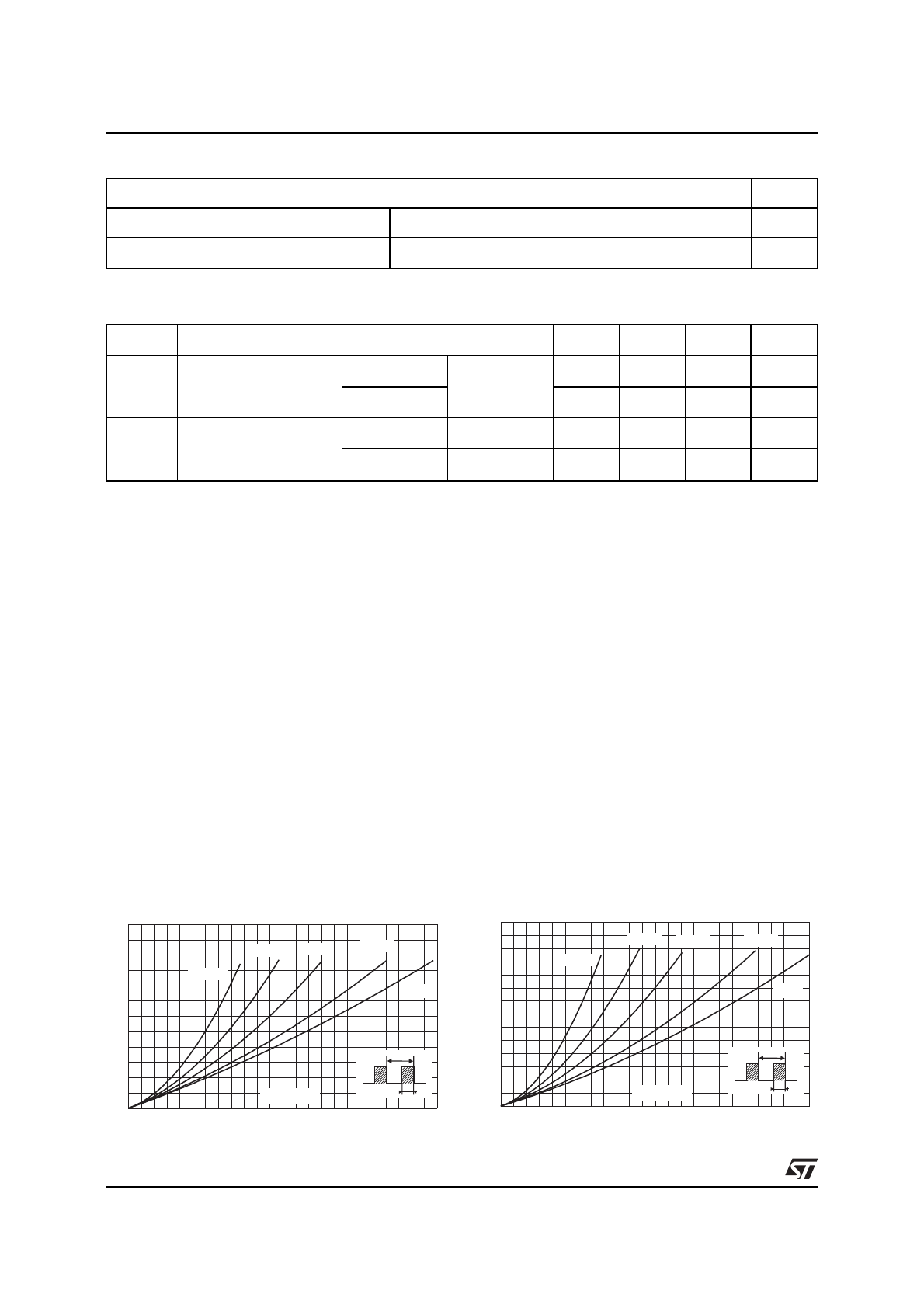
0.0 0.1 0.2 0.3 0.4 0.5 0.6 0.7 0.8 0.9 1.0 1.1 1.2
0.0
0.1
0.2
0.3
0.4
0.5
0.6
PF(av)(W)
IF(av) (A)
T
δ
=tp/T
tp
δ
= 0.2
δ
= 0.5
δ
= 1
δ
= 0.05
δ
= 0.1
Fig. 1: Average forward power dissipation versus
average forward current (1N5817/1N5818).
0.0 0.1 0.2 0.3 0.4 0.5 0.6 0.7 0.8 0.9 1.0 1.1 1.2
0.0
0.1
0.2
0.3
0.4
0.5
0.6
0.7
PF(av)(W)
IF(av) (A)
T
δ
=tp/T
tp
δ
= 0.2
δ
= 0.5
δ
= 1
δ
= 0.05
δ
= 0.1
Fig. 2: Average forward power dissipation versus
average forward current (1N5819).
1N581x
2/5
0
25
50
75
100
125
150
0.0
0.2
0.4
0.6
0.8
1.0
1.2
IF(av)(A)
Tamb(°C)
T
δ
=tp/T
tp
Rth(j-a)=100°C/W
Rth(j-a)=Rth(j-l)=45°C/W
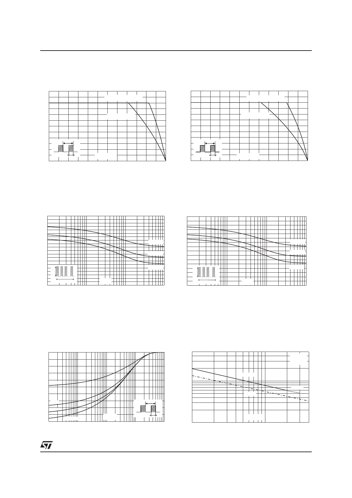
Fig. 2-1: Average forward current versus ambient
temperature (
δ
=0.5) (1N5817/1N5818).
1E-3
1E-2
1E-1
1E+0
0
1
2
3
4
5
6
7
8
9
10
IM(A)
t(s)
Ta=100°C
Ta=75°C
Ta=25°C
I
M
t
δ
=0.5
Fig. 3-1: Non repetitive surge peak forward
current versus overload duration
(maximum values) (1N5817/1N5818).
1E-1
1E+0
1E+1
1E+2
1E+3
0.0
0.2
0.4
0.6
0.8
1.0
Zth(j-a)/Rth(j-a)
T
δ
=tp/T
tp
tp(s)
δ
= 0.1
δ
= 0.2
δ
= 0.5
Single pulse
Fig. 4: Relative variation of thermal impedance
junction to ambient versus pulse duration (epoxy
printed circuit board, e(Cu)=35mm, recommended
pad layout).
0
25
50
75
100
125
150
0.0
0.2
0.4
0.6
0.8
1.0
1.2
IF(av)(A)
Tamb(°C)
T
δ
=tp/T
tp
Rth(j-a)=100°C/W
Rth(j-a)=Rth(j-l)=45°C/W
Fig. 2-2: Average forward current versus ambient
temperature (
δ
=0.5) (1N5819).
1E-3
1E-2
1E-1
1E+0
0
1
2
3
4
5
6
7
8
IM(A)
t(s)
Ta=100°C
Ta=75°C
Ta=25°C
I
M
t
δ
=0.5
Fig. 3-2: Non repetitive surge peak forward
current versus overload duration
(maximum values) (1N5819).
1
2
5
10
20
40
10
20
50
100
200
500
C(pF)
VR(V)
1N5819
1N5817
1N5818
F=1MHz
Tj=25°C
Fig. 5: Junction capacitance versus reverse
voltage applied (typical values).
1N581x
3/5
0
5
10
15
20
25
30
1E-3
1E-2
1E-1
1E+0
1E+1
IR(mA)
1N5817
1N5818
VR(V)
Tj=100°C
Tj=25°C
Tj=125°C
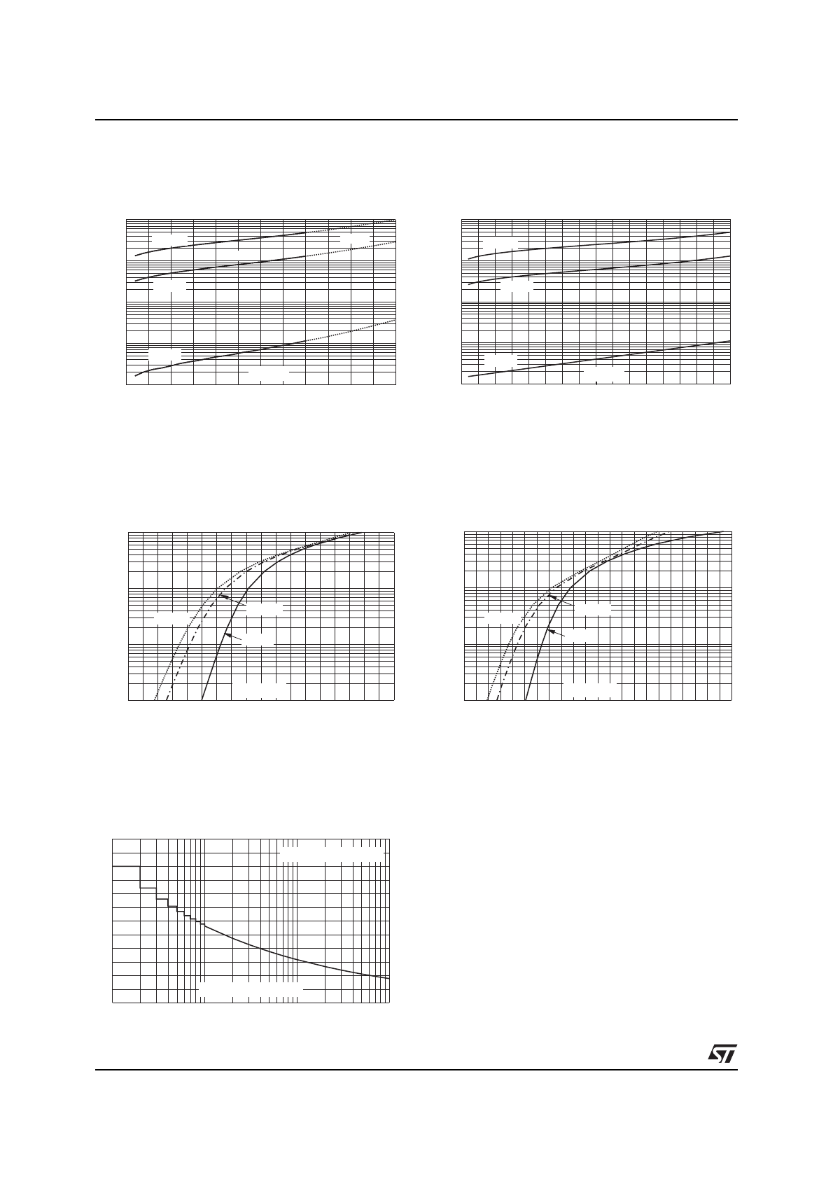
Fig. 6-1: Reverse leakage current versus reverse
voltage applied (typical values) (1N5817/1N5818).
0
5
10
15
20
30
35
40
1E-3
1E-2
1E-1
1E+0
1E+1
IR(mA)
VR(V)
Tj=100°C
Tj=25°C
Tj=125°C
Fig. 6-2: Reverse leakage current versus reverse
voltage applied (typical values) (1N5819).
0.0
0.1
0.2
0.3
0.4
0.5
0.6
0.7
0.8
0.9
0.01
0.10
1.00
10.00
IFM(A)
VFM(V)
Tj=25°C
Tj=100°C
Tj=125°C
Fig. 7-1: Forward voltage drop versus forward
current (typical values) (1N5817/1N5818).
0.0 0.1 0.2 0.3 0.4 0.5 0.6 0.7 0.8 0.9 1.0 1.1
0.01
0.10
1.00
10.00
IFM(A)
VFM(V)
Tj=25°C
Tj=100°C
Tj=125°C
Fig. 7-2: Forward voltage drop versus forward
current (typical values) (1N5819).
1
10
100
1000
0
5
10
15
20
25
30
IFSM(A)
Number of cycles
F=50Hz
Tj initial=25°C
Fig. 8: Non repetitive surge peak forward current
versus number of cycles.
1N581x
4/5
Information furnished is believed to be accurate and reliable. However, STMicroelectronics assumes no responsibility for the consequences of
use of such information nor for any infringement of patents or other rights of third parties which may result from its use. No license is granted by
implication or otherwise under any patent or patent rights of STMicroelectronics. Specifications mentioned in this publication are subject to
change without notice. This publication supersedes and replaces all information previously supplied.
STMicroelectronics products are not authorized for use as critical components in life support devices or systems without express written ap-
proval of STMicroelectronics.
The ST logo is a registered trademark of STMicroelectronics
© 1999 STMicroelectronics - Printed in Italy - All rights reserved.
STMicroelectronics GROUP OF COMPANIES
Australia - Brazil - China - Finland - France - Germany - Hong Kong - India - Italy - Japan - Malaysia
Malta - Morocco - Singapore - Spain - Sweden - Switzerland - United Kingdom - U.S.A.
http://www.st.com
Ordering type
Marking
Package
Weight
Base qty
Delivery mode
1N581x
Part number
cathode ring
DO41
0.34g
2000
Ammopack
1N581xRL
Part number
cathode ring
DO41
0.34g
5000
Tape & reel
Epoxy meets UL94,V0
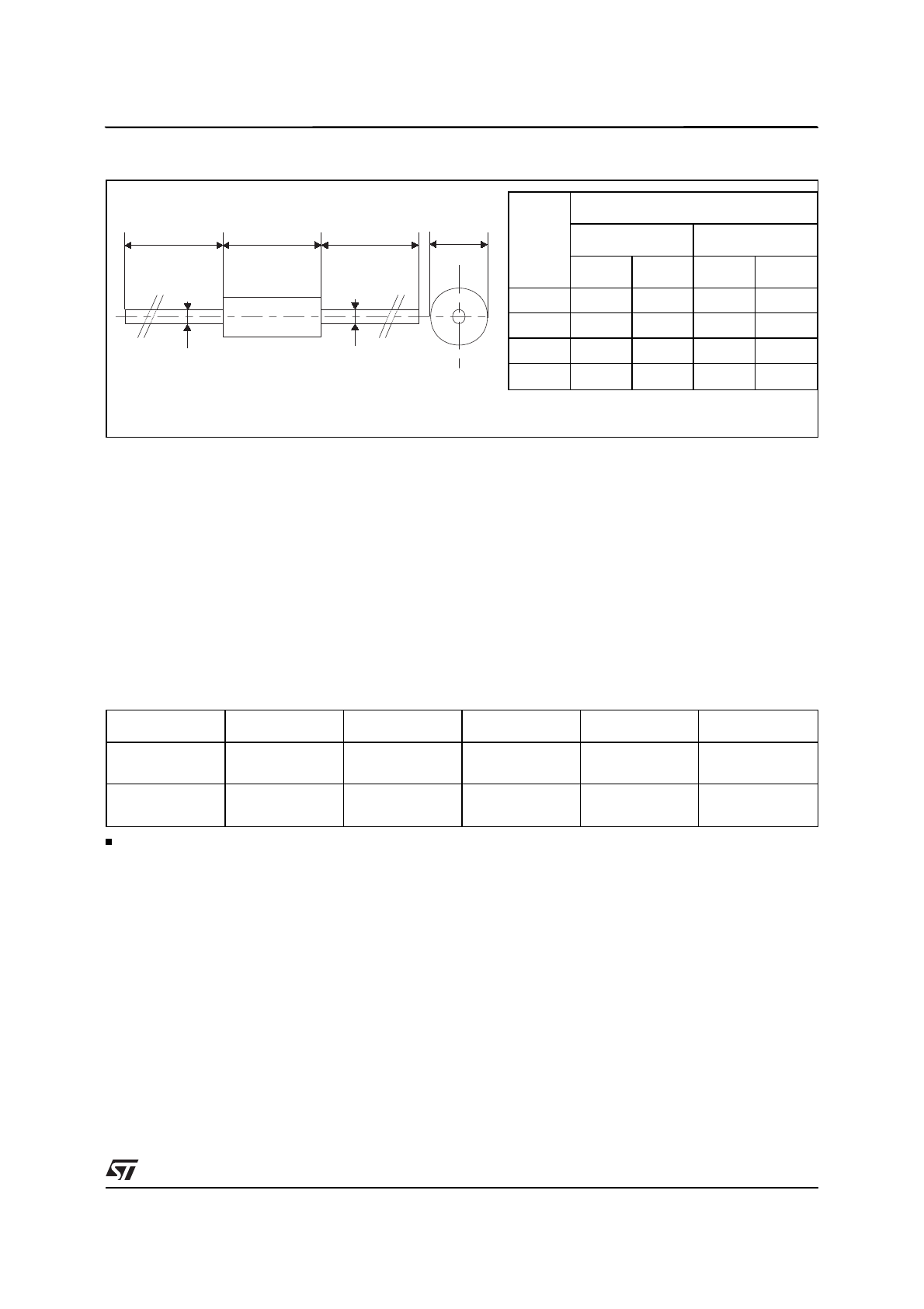
PACKAGE MECHANICAL DATA
DO41 plastic
C
A
B
O
/
O
/
D
O
/
D
C
REF.
DIMENSIONS
Millimeters
Inches
Min.
Max.
Min.
Max.
A
4.1
5.2
0.16
0.205
B
2
2.7
0.08
0.107
C
25.4
1
D
0.71
0.86
0.028
0.034
1N581x
5/5