

ST10R163
16-BIT MCU
USER MANUAL
FEBRUARY 1996
1

2
USE IN LIFE SUPPORT DEVICES OR SYSTEMS MUST BE EXPRESSLY AUTHORIZED.
SGS-THOMSON PRODUCTS ARE NOT AUTHORIZED FOR USE AS CRITICAL COMPONENTS IN LIFE SUPPORT
DEVICES OR SYSTEMS WITHOUT THE EXPRESS WRITTEN APPROVAL OF SGS-THOMSON Microelectronics.
As used herein:
1. Life support devices or systems are those which (a)
are intended for surgical implant into the body, or (b)
support or sustain life, and whose failure to perform,
when properly used in accordance with instructions for
use provided with the product, can be reasonably ex-
pected to result in significant injury to the user.
2. A critical component is any component of a life sup-
port device or system whose failure to perform can rea-
sonably be expected to cause the failure of the life
support device or system, or to affect its safety or effec-
tiveness.

III
Table of Contents
1 - ARCHITECTURAL OVERVIEW . . . . . . . . . . . . . . . . . . . . . . . . . . . . . . . . . 9
1.1 BASIC CPU CONCEPTS AND OPTIMIZATION . . . . . . . . . . . . . . . . . . . . . . . . . . . . . . . . 10
1.2 THE ON-CHIP SYSTEM RESOURCES . . . . . . . . . . . . . . . . . . . . . . . . . . . . . . . . . . . . . . 13
1.3 THE ON-CHIP PERIPHERAL BLOCKS. . . . . . . . . . . . . . . . . . . . . . . . . . . . . . . . . . . . . . . 15
1.4 THE APPLICATION-SPECIFIC SYNCHRONOUS SERIAL PORT . . . . . . . . . . . . . . . . . . 17
1.5 PROTECTED BITS . . . . . . . . . . . . . . . . . . . . . . . . . . . . . . . . . . . . . . . . . . . . . . . . . . . . . .18
2 - MEMORY ORGANIZATION . . . . . . . . . . . . . . . . . . . . . . . . . . . . . . . . . . . 19
2.1 INTERNAL RAM AND SFR AREA . . . . . . . . . . . . . . . . . . . . . . . . . . . . . . . . . . . . . . . . . . . 21
2.2 EXTERNAL MEMORY SPACE . . . . . . . . . . . . . . . . . . . . . . . . . . . . . . . . . . . . . . . . . . . . . 26
2.3 CROSSING MEMORY BOUNDARIES . . . . . . . . . . . . . . . . . . . . . . . . . . . . . . . . . . . . . . . 26
3 - CENTRAL PROCESSING UNIT . . . . . . . . . . . . . . . . . . . . . . . . . . . . . . . . 27
3.1 INSTRUCTION PIPELINING . . . . . . . . . . . . . . . . . . . . . . . . . . . . . . . . . . . . . . . . . . . . . . . 28
3.2 BIT-HANDLING AND BIT-PROTECTION . . . . . . . . . . . . . . . . . . . . . . . . . . . . . . . . . . . . . 33
3.3 INSTRUCTION STATE TIMES . . . . . . . . . . . . . . . . . . . . . . . . . . . . . . . . . . . . . . . . . . . . . 34
3.4 CPU SPECIAL FUNCTION REGISTERS . . . . . . . . . . . . . . . . . . . . . . . . . . . . . . . . . . . . . 35
4 - INTERRUPT AND TRAP FUNCTIONS . . . . . . . . . . . . . . . . . . . . . . . . . . 53
4.1 INTERRUPT SYSTEM STRUCTURE . . . . . . . . . . . . . . . . . . . . . . . . . . . . . . . . . . . . . . . . 54
4.2 OPERATION OF THE PEC CHANNELS . . . . . . . . . . . . . . . . . . . . . . . . . . . . . . . . . . . . . . 61
4.3 PRIORITIZATION OF INTERRUPT AND PEC SERVICE REQUESTS . . . . . . . . . . . . . . 64
4.4 SAVING THE STATUS DURING INTERRUPT SERVICE. . . . . . . . . . . . . . . . . . . . . . . . . 66
4.5 SAVING THE STATUS DURING INTERRUPT SERVICE. . . . . . . . . . . . . . . . . . . . . . . . . 67
4.6 INTERRUPT RESPONSE TIMES . . . . . . . . . . . . . . . . . . . . . . . . . . . . . . . . . . . . . . . . . . . 67
4.7 INTERRUPT RESPONSE TIMES . . . . . . . . . . . . . . . . . . . . . . . . . . . . . . . . . . . . . . . . . . . 68
4.8 EXTERNAL INTERRUPTS . . . . . . . . . . . . . . . . . . . . . . . . . . . . . . . . . . . . . . . . . . . . . . . .71
4.9
TRAP FUNCTIONS . . . . . . . . . . . . . . . . . . . . . . . . . . . . . . . . . . . . . . . . . . . . . . . . . . . . . .73
5 - PARALLEL PORTS . . . . . . . . . . . . . . . . . . . . . . . . . . . . . . . . . . . . . . . . . 77
5.1 PORT 0 . . . . . . . . . . . . . . . . . . . . . . . . . . . . . . . . . . . . . . . . . . . . . . . . . . . . . . . . . . . . . . .80
5.2 PORT 1 . . . . . . . . . . . . . . . . . . . . . . . . . . . . . . . . . . . . . . . . . . . . . . . . . . . . . . . . . . . . . . .83
5.3 PORT 2 . . . . . . . . . . . . . . . . . . . . . . . . . . . . . . . . . . . . . . . . . . . . . . . . . . . . . . . . . . . . . . .86
5.4 PORT 3 . . . . . . . . . . . . . . . . . . . . . . . . . . . . . . . . . . . . . . . . . . . . . . . . . . . . . . . . . . . . . . .89
5.1 PORT 4 . . . . . . . . . . . . . . . . . . . . . . . . . . . . . . . . . . . . . . . . . . . . . . . . . . . . . . . . . . . . . . .94
5.5 PORT 5 . . . . . . . . . . . . . . . . . . . . . . . . . . . . . . . . . . . . . . . . . . . . . . . . . . . . . . . . . . . . . . .98
5.6 PORT 6 . . . . . . . . . . . . . . . . . . . . . . . . . . . . . . . . . . . . . . . . . . . . . . . . . . . . . . . . . . . . . .100
6 - DEDICATED PINS . . . . . . . . . . . . . . . . . . . . . . . . . . . . . . . . . . . . . . . . . 105
7 - EXTERNAL BUS INTERFACE . . . . . . . . . . . . . . . . . . . . . . . . . . . . . . . . 107
7.1
SINGLE CHIP MODE . . . . . . . . . . . . . . . . . . . . . . . . . . . . . . . . . . . . . . . . . . . . . . . . . . .108
7.2 EXTERNAL BUS MODES . . . . . . . . . . . . . . . . . . . . . . . . . . . . . . . . . . . . . . . . . . . . . . . . 108
3

IV
Table of Contents
7.3 PROGRAMMABLE BUS CHARACTERISTICS . . . . . . . . . . . . . . . . . . . . . . . . . . . . . . . . 114
7.4 READY CONTROLLED BUS CYCLES . . . . . . . . . . . . . . . . . . . . . . . . . . . . . . . . . . . . . . 119
7.5 CONTROLLING THE EXTERNAL BUS CONTROLLER. . . . . . . . . . . . . . . . . . . . . . . . . 120
7.6 EBC IDLE STATE . . . . . . . . . . . . . . . . . . . . . . . . . . . . . . . . . . . . . . . . . . . . . . . . . . . . . .127
7.7 EXTERNAL BUS ARBITRATION . . . . . . . . . . . . . . . . . . . . . . . . . . . . . . . . . . . . . . . . . . . 127
7.8 THE XBUS INTERFACE . . . . . . . . . . . . . . . . . . . . . . . . . . . . . . . . . . . . . . . . . . . . . . . . .130
8 - GENERAL PURPOSE TIMER UNITS . . . . . . . . . . . . . . . . . . . . . . . . . . 131
8.1 TIMER BLOCK GPT1 . . . . . . . . . . . . . . . . . . . . . . . . . . . . . . . . . . . . . . . . . . . . . . . . . . .131
8.2 TIMER BLOCK GPT2 . . . . . . . . . . . . . . . . . . . . . . . . . . . . . . . . . . . . . . . . . . . . . . . . . . .145
9 - ASYNCHRONOUS/SYNCHRONOUS SERIAL INTERFACE . . . . . . . . 159
9.1 ASYNCHRONOUS OPERATION . . . . . . . . . . . . . . . . . . . . . . . . . . . . . . . . . . . . . . . . . . 161
9.2 SYNCHRONOUS OPERATION . . . . . . . . . . . . . . . . . . . . . . . . . . . . . . . . . . . . . . . . . . . . 164
9.3 HARDWARE ERROR DETECTION CAPABILITIES . . . . . . . . . . . . . . . . . . . . . . . . . . . . 165
9.4 ASC0 BAUD RATE GENERATION . . . . . . . . . . . . . . . . . . . . . . . . . . . . . . . . . . . . . . . . . 166
9.5 ASC0 INTERRUPT CONTROL . . . . . . . . . . . . . . . . . . . . . . . . . . . . . . . . . . . . . . . . . . . . 168
10 - SYNCHRONOUS SERIAL PORT . . . . . . . . . . . . . . . . . . . . . . . . . . . . . 171
11 - WATCHDOG TIMER . . . . . . . . . . . . . . . . . . . . . . . . . . . . . . . . . . . . . . 187
12 - SYSTEM RESET . . . . . . . . . . . . . . . . . . . . . . . . . . . . . . . . . . . . . . . . . 191
12.1 THE ST10R163’S PINS AFTER RESET . . . . . . . . . . . . . . . . . . . . . . . . . . . . . . . . . . . . . 193
12.2 RESET OUTPUT PIN . . . . . . . . . . . . . . . . . . . . . . . . . . . . . . . . . . . . . . . . . . . . . . . . . . .194
12.3 WATCHDOG TIMER OPERATION AFTER RESET . . . . . . . . . . . . . . . . . . . . . . . . . . . . 194
12.4 RESET VALUES FOR THE ST10R163 REGISTERS . . . . . . . . . . . . . . . . . . . . . . . . . . . 194
12.5 THE INTERNAL RAM AFTER RESET. . . . . . . . . . . . . . . . . . . . . . . . . . . . . . . . . . . . . . . 194
12.6 PORTS AND EXTERNAL BUS CONFIGURATION DURING RESET. . . . . . . . . . . . . . . 194
12.7 APPLICATION-SPECIFIC INITIALIZATION ROUTINE. . . . . . . . . . . . . . . . . . . . . . . . . . 195
13 - POWER REDUCTION MODES . . . . . . . . . . . . . . . . . . . . . . . . . . . . . . 199
13.1 IDLE MODE . . . . . . . . . . . . . . . . . . . . . . . . . . . . . . . . . . . . . . . . . . . . . . . . . . . . . . . . . . .199
13.2 POWER DOWN MODE . . . . . . . . . . . . . . . . . . . . . . . . . . . . . . . . . . . . . . . . . . . . . . . . . . 200
13.3 STATUS OF OUTPUT PINS DURING IDLE AND POWER DOWN MODE . . . . . . . . . . 201
14 - SYSTEM CLOCK GENERATOR . . . . . . . . . . . . . . . . . . . . . . . . . . . . . 203
14.1 PLL OPERATION . . . . . . . . . . . . . . . . . . . . . . . . . . . . . . . . . . . . . . . . . . . . . . . . . . . . . . .203
14.2 OPERATION WITHOUT PLL . . . . . . . . . . . . . . . . . . . . . . . . . . . . . . . . . . . . . . . . . . . . . . 204
4

V
Table of Contents
15 - SYSTEM PROGRAMMING . . . . . . . . . . . . . . . . . . . . . . . . . . . . . . . . . 205
15.1 INSTRUCTIONS PROVIDED AS SUBSETS OF INSTRUCTIONS. . . . . . . . . . . . . . . . . 205
15.2 MULTIPLICATION AND DIVISION . . . . . . . . . . . . . . . . . . . . . . . . . . . . . . . . . . . . . . . . . 206
15.3 BCD CALCULATIONS . . . . . . . . . . . . . . . . . . . . . . . . . . . . . . . . . . . . . . . . . . . . . . . . . . . 207
15.4 STACK OPERATIONS . . . . . . . . . . . . . . . . . . . . . . . . . . . . . . . . . . . . . . . . . . . . . . . . . . . 207
15.5 REGISTER BANKING . . . . . . . . . . . . . . . . . . . . . . . . . . . . . . . . . . . . . . . . . . . . . . . . . . .210
15.6 PROCEDURE CALL ENTRY AND EXIT . . . . . . . . . . . . . . . . . . . . . . . . . . . . . . . . . . . . . 211
15.7 TABLE SEARCHING . . . . . . . . . . . . . . . . . . . . . . . . . . . . . . . . . . . . . . . . . . . . . . . . . . . .213
15.8 PERIPHERAL CONTROL AND INTERFACE . . . . . . . . . . . . . . . . . . . . . . . . . . . . . . . . . 213
15.9 FLOATING POINT SUPPORT . . . . . . . . . . . . . . . . . . . . . . . . . . . . . . . . . . . . . . . . . . . . . 213
15.10TRAP/INTERRUPT ENTRY AND EXIT . . . . . . . . . . . . . . . . . . . . . . . . . . . . . . . . . . . . . 213
15.11UNSEPARABLE INSTRUCTION SEQUENCES . . . . . . . . . . . . . . . . . . . . . . . . . . . . . . 214
15.12OVERRIDING THE DPP ADDRESSING MECHANISM. . . . . . . . . . . . . . . . . . . . . . . . . 214
16 - REGISTER SET . . . . . . . . . . . . . . . . . . . . . . . . . . . . . . . . . . . . . . . . . . 217
16.1 CPU GENERAL PURPOSE REGISTERS (GPRS) . . . . . . . . . . . . . . . . . . . . . . . . . . . . . 218
16.2 SPECIAL FUNCTION REGISTERS ORDERED BY NAME. . . . . . . . . . . . . . . . . . . . . . . 220
16.3 REGISTERS ORDERED BY ADDRESS . . . . . . . . . . . . . . . . . . . . . . . . . . . . . . . . . . . . . 223
17 - INSTRUCTION SET SUMMARY . . . . . . . . . . . . . . . . . . . . . . . . . . . . . 227
18 - DEVICE SPECIFICATION . . . . . . . . . . . . . . . . . . . . . . . . . . . . . . . . . . 231
5

VI
INTRODUCTION
High Performance 16-Bit CPU With Four-Stage
Pipeline
■
80 ns minimum instruction cycle time, with most
instructions executed in 1 cycle
■
400 ns multiplication (16-bit *16-bit), 800 ns
division (32-bit/16-bit)
■
Multiple high bandwidth internal data buses
■
Register based design with multiple variable
register banks
■
Single cycle context switching support
■
16 MBytes linear address space for code and
data (von Neumann architecture)
■
System stack cache support with automatic
stack overflow/underflow detection
Control Oriented Instruction Set with High
Efficiency
■
Bit, byte, and word data types
■
Flexible and efficient addressing modes for high
code density
■
Enhanced boolean bit manipulation with direct
addressability of 4 Kbits
for peripheral control and user defined flags
■
Hardware traps to identify exception conditions
during runtime
■
HLL support for semaphore operations and
efficient data access
Integrated On-chip Memory
■
2 KByte internal RAM for variables, register
banks, system stack and code
External Bus Interface
■
Multiplexed
or
non-multiplexed
bus
configurations
■
Segmentation capability and chip select signal
generation
■
8-bit or 16-bit data bus
■
Programmable
Bus
configuration
for
five
programmable address areas
16-Priority-Level Interrupt System
■
28 interrupt nodes with separate interrupt
vectors
■
200/400 ns typical/maximum interrupt latency in
case of internal program execution
■
Fast external interrupts
8-Channel Peripheral Event Controller (PEC)
■
Interrupt driven single cycle data transfer
■
Transfer count option (standard CPU interrupt
after a programmable
number of PEC transfers)
■
Eliminates overhead of saving and restoring
system state for interrupt requests
Intelligent On-chip Peripheral Subsystems
■
2 Multifunctional General Purpose Timer Units
GPT1: three 16-bit timers/ counters, 320 ns
maximum resolution
GPT2: two 16-bit timers/counters, 160 ns
maximum resolution
■
Asynchronous/Synchronous
Serial
Channel
(USART)
with baud rate generator, parity, framing, and
overrun error detection
■
High Speed Synchronous Serial Channel
programmable data length and shift direction
■
Watchdog
Timer with
programmable
time
intervals
■
Bootstrap
Loader
for
flexible
system
initialization
77 IO Lines With Individual Bit Addressability
■
Tri-stated in input mode
■
Push/pull or open drain output mode
Different Temperature Ranges
■
0 to +70
°
C, –40 to +85
°
C
Multifunctional CMOS Process
■
Low Power CMOS Technology, including power
saving Idle and Power Down modes
■
100-Pin
Plastic
Quad
Flat
Pack
(PQFP)
Package
■
EIAJ standard, 0.65 mm (25.6 mil) lead spacing,
surface mount technology
6

VII
FEATURES
Complete Development Support
A variety of software and hardware development
tools for the SGS-THOMSON family of 16-bit
microcontrollers is available from experienced
international tool suppliers. The high quality and
reliability of these tools is already proven in many
applications
and
by many
users.
The tool
environment
for
the
SGS-THOMSON
16-bit
microcontrollers includes the following tools:
■
Compilers (C, MODULA2, FORTH)
■
Macro-Assemblers, Linkers, Locaters, Library
Managers, Format-Converters
■
Architectural Simulators
■
HLL debuggers
■
Real-Time operating systems
■
VHDL chip models
■
In-Circuit Emulators (based on bondout or
standard chips)
■
Plug-In emulators
■
Emulation and Clip-Over adapters, production
sockets
■
Logic Analyzer disassemblers
■
Evaluation Boards with monitor programs
■
Industrial
boards (also
for CAN, FUZZY,
PROFIBUS, FORTH applications)
■
Network driver software (CAN, PROFIBUS)
Abbreviations
The following acronyms and termini are used
within this document:
ALE . . Address Latch Enable
ALU . . Arithmetic and Logic Unit
ASC . . Asynchronous/synchronous Serial
Controller
CAN . . . Controller Area Network (License Bosch)
CISC . Complex Instruction Set Computing
CMOS Complementary Metal Oxide Silicon
CPU . . Central Processing Unit
EBC . . External Bus Controller
ESFR . Extended Special Function Register
Flash . Non-volatile memory that may be
electrically erased
GPR . . General Purpose Register
GPT . . General Purpose Timer unit
HLL . . High Level Language
IO . . . . Input / Output
PEC . . Peripheral Event Controller
PLA . . Programmable Logic Array
RAM . . Random Access Memory
RISC . Reduced Instruction Set Computing
ROM. . Read Only Memory
SFR . . Special Function Register
SSC . . Synchronous Serial Controller
XBUS . . Internal representation of the External Bus
7

VIII
INTRODUCTION
Notes:
8
February 1996
1/10
This is advance information from SGS-TH OMSON. Details are subject tochange without notice.
ST10R163
User Manual
1 - ARCHITECTURAL OVERVIEW
The architecture of the ST10R163 combines the
advantages of both RISC and CISC processors in
a very well-balanced way. The sum of the features
which are combined result in a high performance
microcontroller, which is the right choice not only
for today’s applications, but also for future engi-
neering challenges. The ST10R163 not only inte-
grates a powerful CPU core and a set of peripher-
al units into one chip, but also connects the units
in a very efficient way. One of the four buses used
concurrently on the ST10R163 is the XBUS, an in-
ternal representation of the external bus interface.
This bus provides a standardized method of inte-
grating application-specific peripherals to produce
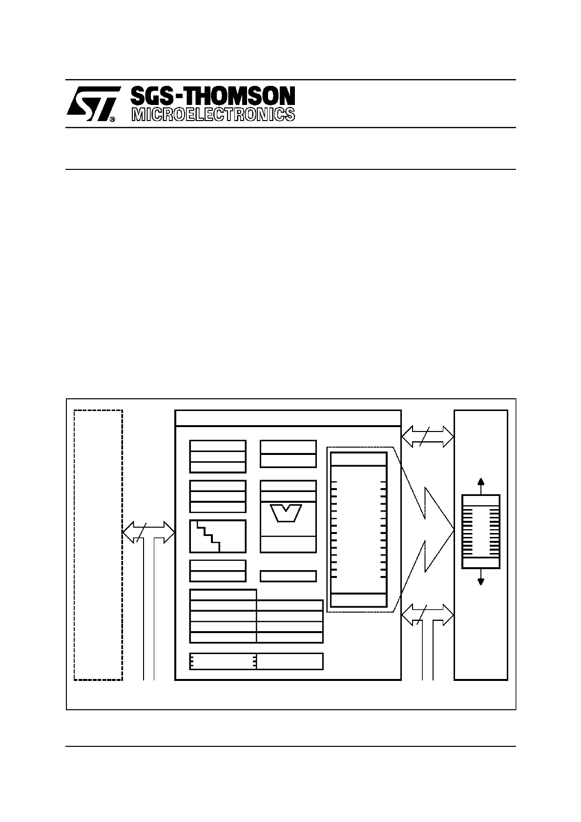
derivates of the standard ST10R163.
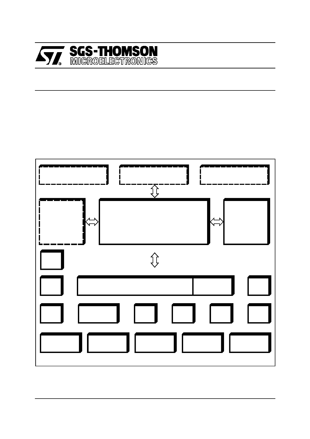
Figure 1-1. ST10R163 Functional Block Diagram
VR02078B
OSC
WDT
Interrupt Controller
P1
P3
P4
P6
P2
PEC
SSP
RAM
Area
ROM
Internal
Core
CPU
GPT1
P5
GPT2
P0
ASC
BUS CTL
XBUS-Module
XBUS-Module
PLL
9
2/10
1 - ARCHITECTURAL OVERVIEW (ST10R163)
1.1 BASIC CPU CONCEPTS AND OPTIMIZATION
The main core of the CPU consists of a 4-stage in-
struction pipeline, a 16-bit arithmetic and logic unit
(ALU) and dedicated SFRs. Additional hardware
has been spent for a separate multiply and divide
unit a bit-mask generator and a barrel shifter.
To meet the demand for greater performance and
flexibility, a number of areas has been optimized
in the processor core. Functional blocks in the
CPU core are controlled by signals from the in-
struction decode logic. These are summarized be-
low, and described in detail in the following sec-
tions:
1) High Instruction Bandwidth / Fast Execution
2) High Function 8-bit and 16-bit Arithmetic and
Logic Unit
3) Extended Bit Processing and Peripheral Con-
trol
4) High Performance Branch-, Call-, and Loop
Processing
5) Consistent and Optimized Instruction Formats
6) Programmable Multiple Priority Interrupt Struc-
ture
Figure 1-2. CPU Block Diagram
VR02080B
CPU
SP
STKOV
STKUN
Instr.Reg.
Instr.Ptr.
Exec.Unit
4-Stage
Pipeline
MDH
MDL
PSW
SYSCON
Context Ptr.
Mul/Div-HW
Gen
-
R15
R0
General
Purpose
Registers
Bit-Mask
Barrel Shifter
ALU
(16-bit)
Data PagePtr.
CodeSeg.Ptr.
RAM
R15
R0
ROM
16
16
32
BUSCON 0
BUSCON 1
BUSCON 2
BUSCON 3
BUSCON 4
ADDRSEL 4
ADDRSEL 3
ADDRSEL 2
ADDRSEL 1
1 KByte
10

3/10
1 - ARCHITECTURAL OVERVIEW (ST10R163)
BASIC CPU CONCEPTS AND OPTIMIZATION(Cont’d)
Hiigh Instruction Bandwidth / Fast Execution
Based on the hardware provisions, most of the
ST10R163’s instructions can be exected in just
one machine cycle, which requires 100 ns at 20
MHz CPU clock (resp. 80 ns at 25 MHz CPU
clock). For example, shift and rotate instructions
are always processed within one machine cycle,
independent of the number of bits to be shifted.
Branch-, multiply- and divide instructions normally
take more than one machine cycle. These instruc-
tions, however, have also been optimized. For ex-
ample, branch instructions only require an addi-
tional machine cycle, when a branch is taken, and
most branches taken in loops require no additional
machine cycles at all, due to the ‘Jump Cache’.
A 32-bit / 16-bit division takes 1
µ
s (resp. 0.8
µ
s),
a 16-bit
*
16-bit multiplication takes 0.5
µ
s (resp.
0.4
µ
s) at 20 MHz (resp. 25 MHz) CPU clock.
The instruction cycle time has been dramatically
reduced through the use of instruction pipelining.
This technique allows the core CPU to process
portions of multiple sequential instruction stages
in parallel. The following four stage pipeline pro-
vides the optimum balancing for the CPU core:
FETCH: In this stage, an instruction is fetched
from the internal ROM or RAM or from the external
memory, based on the current IP value.
DECODE: In this stage, the previously fetched in-
struction is decoded and the required operands
are fetched.
EXECUTE: In this stage, the specified operation is
performed on the previously fetched operands.
WRITE BACK: In this stage, the result is written to
the specified location.
If this technique were not used, each instruction
would require four machine cycles. This increased
performance allows a greater number of tasks and
interrupts to be processed.
Instruction Decoder
Instruction decoding is primarily generated from
PLA outputs based on the selected opcode. No
microcode is used and each pipeline stage re-
ceives control signals staged in control registers
from the decode stage PLAs. Pipeline holds are
primarily caused by wait states for external mem-
ory accesses and cause the holding of signals in
the control registers. Multiple-cycle instructions
are performed through instruction injection and
simple internal state machines which modify re-
quired control signals.
High Function 8-bit and 16-bit Arithmetic and Log-
ic Unit
All standard arithmetic and logical operations are
performed in a 16-bit ALU. In addition, for byte op-
erations, signals are provided from bits six and
seven of the ALU result to correctly set the condi-
tion flags. Multiple precision arithmetic is provided
through a ’CARRY-IN’ signal to the ALU from pre-
viously calculated portions of the desired opera-
tion. Most internal execution blocks have been op-
timized to perform operations on either 8-bit or 16-
bit quantities. Once the pipeline has been filled,
one instruction is completed per machine cycle,
except for multiply and divide. An advanced Booth
algorithm has been incorporated to allow four bits
to be multiplied and two bits to be divided per ma-
chine cycle. Thus, these operations use two cou-
pled 16-bit registers, MDL and MDH, and require
four and nine machine cycles, respectively, to per-
form a 16-bit by 16-bit (or 32-bit by 16-bit) calcula-
tion plus one machine cycle to setup and adjust
the operands and the result. Even these longer
multiply and divide instructions can be interrupted
during their execution to allow for very fast inter-
rupt response. Instructions have also been provid-
ed to allow byte packing in memory while provid-
ing sign extension of bytes for word wide arithme-
tic operations. The internal bus structure also al-
lows transfers of bytes or words to or from periph-
erals based on the peripheral requirements.
A set of consistent flags is automatically updated
in the PSW after each arithmetic, logical, shift, or
movement operation. These flags allow branching
on specific conditions. Support for both signed
and unsigned arithmetic is provided through user-
specifiable branch tests. These flags are also pre-
served automatically by the CPU upon entry into
an interrupt or trap routine.
All targets for branch calculations are also com-
puted in the central ALU.
A 16-bit barrel shifter provides multiple bit shifts in
a single cycle. Rotates and arithmetic shifts are
also supported.
Extended
Bit
Processing
and
Peripheral
Control
A large number of instructions has been dedicated
to bit processing. These instructions provide effi-
cient control and testing of peripherals while en-
hancing data manipulation. Unlike other microcon-
trollers, these instructions provide direct access to
two operands in the bit-addressable space without
requiring to move them into temporary flags.
The same logical instructions available for words
and bytes are also supported for bits. This allows
the user to compare and modify a control bit for a
peripheral in one instruction. Multiple bit shift in-
structions have been included to avoid long in-
struction streams of single bit shift operations.
These are also performed in a single machine cy-
cle.
11

4/10
1 - ARCHITECTURAL OVERVIEW (ST10R163)
BASIC CPU CONCEPTS AND OPTIMIZATION(Cont’d)
n addition, bit field instructions have been provid-
ed, which allow the modification of multiple bits
from one operand in a single instruction.
High Performance Branch-, Call-, and Loop
Processing
Due to the high percentage of branching in con-
troller applications, branch instructions have been
optimized to require one extra machine cycle only
when a branch is taken. This is implemented by
precalculating the target address while decoding
the instruction. To decrease loop execution over-
head, three enhancements have been provided:
•
The first solution provides single cycle branch
execution after the first iteration of a loop. Thus,
only one machine cycle is lost during the execu-
tion of the entire loop. In loops which fall through
upon completion, no machine cycles are lost when
exiting the loop. No special instructions are re-
quired to perform loops, and loops are automati-
cally detected during execution of branch instruc-
tions.
•
The second loop enhancement allows the detec-
tion of the end of a table and avoids the use of two
compare instructions embedded in loops. One
simply places the lowest negative number at the
end of the specific table, and specifies branching if
neither this value nor the compared value have
been found. Otherwise the loop is terminated if ei-
ther condition has been met. The terminating con-
dition can then be tested.
•
The third loop enhancement provides a more
flexible solution than the Decrement and Skip on
Zero instruction which is found in other microcon-
trollers. Through the use of Compare and Incre-
ment or Decrement instructions, the user can
make comparisons to any value. This allows loop
counters to cover any range. This is particularly
advantageous in table searching.
Saving of system state is automatically performed
on the internal system stack avoiding the use of in-
structions to preserve state upon entry and exit of
interrupt or trap routines. Call instructions push
the value of the IP on the system stack, and re-
quire the same execution time as branch instruc-
tions.
Instructions have also been provided to support
indirect branch and call instructions. This supports
implementation
of
multiple
CASE
statement
branching in assembler macros and high level lan-
guages.
Consistent and Optimized Instruction Formats
To obtain optimum performance in a pipelined de-
sign, an instruction set has been designed which
incorporates concepts from Reduced Instruction
Set Computing (RISC). These concepts primarily
allow fast decoding of the instructions and oper-
ands while reducing pipeline holds. These con-
cepts, however, do not preclude the use of com-
plex instructions, which are required by microcon-
troller users. The following goals were used to de-
sign the instruction set:
1) Provide powerful instructions to perform opera-
tions which currently require sequences of
instructions and are frequently used. Avoid
transfer into and out of temporary registers
such as accumulators and carry bits. Perform
tasks in parallel such as saving state upon
entry into interrupt routines or subroutines.
2) Avoid complex encoding schemes by placing
operands in consistent fields for each instruc-
tion. Also avoid complex addressing modes
which are not frequently used. This decreases
the instruction decode time while also simplify-
ing the development of compilers and assem-
blers.
3) Provide most frequently used instructions with
one-word instruction formats. All other instruc-
tions are placed into two-word formats. This
allows all instructions to be placed on word
boundaries, which alleviates the need for com-
plex alignment hardware. It also has the benefit
of increasing the range for relative branching
instructions.
The high performance offered by the hardware im-
plementation of the CPU can efficiently be utilized
by
a programmer
via the highly
functional
ST10R163 instruction set which includes the fol-
lowing instruction classes:
•
Arithmetic Instructions
•
Logical Instructions
•
Boolean Bit Manipulation Instructions
•
Compare and Loop Control Instructions
•
Shift and Rotate Instructions
•
Prioritize Instruction
•
Data Movement Instructions
•
System Stack Instructions
•
Jump and Call Instructions
•
Return Instructions
•
System Control Instructions
•
Miscellaneous Instructions
Possible operand types are bits, bytes and words.
Specific instruction support the conversion (exten-
sion) of bytes to words. A variety of direct, indirect
or immediate addressing modes are provided to
specify the required operands.
12

5/10
1 - ARCHITECTURAL OVERVIEW (ST10R163)
BASIC CPU CONCEPTS AND OPTIMIZATION(Cont’d)
Programmable
Multiple
Priority
Interrupt
System
The following enhancements have been included
to allow processing of a large number of interrupt
sources:
1) Peripheral Event Controller (PEC): This proc-
essor is used to off-load many interrupt
requests from the CPU. It avoids the overhead
of entering and exiting interrupt or trap routines
by
performing
single-cycle
interrupt-driven
byte or word data transfers between any two
locations in segment 0 with an optional incre-
ment of either the PEC source or the destina-
tion pointer. Just one cycle is ’stolen’ from the
current CPU activity to perform a PEC service.
2) Multiple Priority Interrupt Controller: This con-
troller allows all interrupts to be placed at any
specified
priority.
Interrupts
may
also
be
grouped, which provides the user with the abil-
ity to prevent similar priority tasks from inter-
rupting each other. For each of the possible
interrupt sources there is a separate control
register, which contains an interrupt request
flag, an interrupt enable flag and an interrupt
priority bitfield. Once having been accepted by
the CPU, an interrupt service can only be inter-
rupted by a higher prioritized service request.
For standard interrupt processing, each of the
possible interrupt sources has a dedicated vec-
tor location.
3) Multiple Register Banks: This feature allows the
user to specify up to sixteen general purpose
registers located anywhere in the internal RAM.
A single one-machine-cycle instruction allows
to switch register banks from one task to
another.
4) Interruptable
Multiple
Cycle
Instructions:
Reduced interrupt latency is provided by allow-
ing multiple-cycle instructions (multiply, divide)
to be interruptable.
With an interrupt response time within a range
from just 250 ns to 500 ns at 20 MHz CPU clock
(resp. 200 ns to 400 ns at 25 MHz CPU clock) (in
case of maximum speed program execution), the
ST10R163 is capable of reacting very fast on non-
deterministic events.
Its fast external interrupt inputs are sampled every
50 ns at 20 MHz CPU clock (resp. 40 ns at 25 MHz
CPU clock) and allow to recognize even very short
external signals.
The ST10R163 also provides an excellent mecha-
nism to identify and to process exceptions or error
conditions that arise during run-time, ’Hardware
Traps’. Hardware traps cause an immediate non-
maskable system reaction which is similiar to a
standard interrupt service (branching to a dedicat-
ed vector table location). The occurrence of a
hardware trap is additionally signified by an indi-
vidual bit in the trap flag register (TFR). Except for
another higher prioritized trap service being in
progress, a hardware trap will interrupt any current
program execution. In turn, hardware trap servic-
es can normally not be interrupted by standard or
PEC interrupts.
Software interrupts are supported by means of the
’TRAP’ instruction in combination with an individu-
al trap (interrupt) number.
1.2 THE ON-CHIP SYSTEM RESOURCES
The ST10R163 controllers provide a number of
powerful system resources designed around the
CPU. The combination of CPU and these resourc-
es results in the high performance of the members
of this controller family.
Peripheral
Event
Controller
(PEC)
and
Interrupt Control
The Peripheral Event Controller allows to respond
to an interrupt request with a single data transfer
(word or byte) which only consumes one instruc-
tion cycle and does not require to save and restore
the machine status. Each interrupt source is prior-
itized every machine cycle in the interrupt control
block. If PEC service is selected, a PEC transfer is
started. If CPU interrupt service is requested, the
current CPU priority level stored in the PSW regis-
ter is tested to determine whether a higher priority
interrupt is currently being serviced. When an in-
terrupt is acknowledged, the current state of the
machine is saved on the internal system stack and
the CPU branches to the system specific vector
for the peripheral.
The PEC contains a set of SFRs which store the
count value and control bits for eight data transfer
channels. In addition, the PEC uses a dedicated
area of RAM which contains the source and desti-
nation addresses. The PEC is controlled similar to
any other peripheral through SFRs containing the
desired configuration of each channel.
An individual PEC transfer counter is implicitly
decremented for each PEC service except when
performing in the continuous transfer mode. When
this counter reaches zero, a standard interrupt is
performed to the vector location related to the cor-
responding source. PEC services are very well
suited, for example, to move register contents
to/from a memory table. The ST10R163 has 8
PEC channels each of which offers such fast inter-
rupt-driven data transfer capabilities.
13

6/10
1 - ARCHITECTURAL OVERVIEW (ST10R163)
THE ON-CHIP SYSTEM RESOURCES(Cont’d)
Memory Areas
The memory space of the ST10R163 is configured
in a Von Neumann architecture which means that
code memory, data memory, registers and IO
ports are organized within the same linear ad-
dress space which covers up to 16 MBytes. The
entire memory space can be accessed bytewise
or wordwise. Particular portions of the on-chip
memory have additionally been made directly bit
addressable.
A 1 KByte 16-bit wide internal RAM provides
fast
access
to
General
Purpose
Registers
(GPRs), user data (variables) and system stack.
The internal RAM may also be used for code. A
unique decoding scheme provides flexible user
register banks in the internal memory while opti-
mizing the remaining RAM for user data.
The CPU disposes of an actual register context
consisting of up to 16 wordwide and/or bytewide
GPRs, which are physically located within the on-
chip RAM area. A Context Pointer (CP) register
determines the base address of the active register
bank to be accessed by the CPU at a time. The
number of register banks is only restricted by the
available internal RAM space. For easy parameter
passing, a register bank may overlap others.
A system stack of up to 512 words is provided as a
storage for temporary data. The system stack is
also located within the on-chip RAM area, and it is
accessed by the CPU via the stack pointer (SP)
register.
Two separate
SFRs,
STKOV
and
STKUN, are implicitly compared against the stack
pointer value upon each stack access for the de-
tection of a stack overflow or underflow.
Hardware detection of the selected memory space
is placed at the internal memory decoders and al-
lows the user to specify any address directly or in-
directly and obtain the desired data without using
temporary registers or special instructions.
For Special Function Registers 1024 Bytes of
the address space are reserved. The standard
Special Function Register area (SFR) uses 512
bytes, while the Extended Special Function Regis-
ter area (ESFR) uses the other 512 bytes.
(E)SFRs are wordwide registers which are used
for controlling and monitoring functions of the dif-
ferent on-chip units. Unused (E)SFR addresses
are reserved for future members of the ST10R163
family with enhanced functionality.
External Bus Interface
In order to meet the needs of designs where more
memory is required than is provided on chip, up to
16 MBytes of external RAM and/or ROM can be
connected to the microcontroller via its external
bus interface. The integrated External Bus Con-
troller (EBC) allows to access external memory
and/or peripheral resources in a very flexible way.
For up to five address areas the bus mode (multi-
plexed / demultiplexed), the data bus width (8-bit /
16-bit) and even the length of a bus cycle (wait-
states, signal delays) can be selected independ-
ently. This allows to access a variety of memory
and peripheral components directly and with max-
imum efficiency. The EBC can control external ac-
cesses in one of the following four different exter-
nal access modes:
– 16-/18-/20-/24-bit Addresses, 16-bit Data, de-
multiplexed
– 16-/18-/20-/24-bit Addresses, 8-bit Data, demul-
tiplexed
– 16-/18-/20-/24-bit Addresses, 16-bit Data, Multi-
plexed
– 16-/18-/20-/24-bit Addresses, 8-bit Data, Multi-
plexed
The demultiplexed bus modes use PORT1 for ad-
dresses and PORT0 for data input/output. The
multiplexed bus modes use PORT0 for both ad-
dresses and data input/output. All modes use
Port 4 for the upper address lines (A16...) if select-
ed.
Important timing characteristics of the external
bus
interface
(waitstates,
ALE
length
and
Read/Write Delay) have been made programma-
ble to allow the user the adaption of a wide range
of different types of memories and/or peripherals.
Access to very slow memories or peripherals is
supported via a particular ’Ready’ function.
For applications which require less than 64
KBytes of address space, a non-segmented mem-
ory model can be selected, where all locations can
be addressed by 16 bits, and thus Port 4 is not
needed as an output for the upper address bits
(A23/A19/A17...A16), as is the case when using
the segmented memory model.
The on-chip XBUS is an internal representation
of the external bus and allows to access integrat-
ed application-specific peripherals/modules in the
same way as external components. It provides a
defined interface for these customized peripher-
als.
14

7/10
1 - ARCHITECTURAL OVERVIEW (ST10R163)
THE ON-CHIP SYSTEM RESOURCES(Cont’d)
Clock Generator
The on-chip clock generator includes a PLL
(Phase Lock Loop) circuit that allows to operate
the ST10R163 on a variety of frequency external
clock while still providing maximum performances.
The PLL multiplies the external clock frequency by
a programmable factor of 1.5, 2, 2.5, 3, 4 or 5. The
PLL also provides fail safe mechanisms which al-
low to detect frequency deviations and to perform
emergency actions in case of an external clock
failure. The PLL may also be disabled, in which
case the ST10R163 will directly run on the exter-
nal input clock divided by 2 or not. The clock gen-
erator provides a CPU clock signal that controls all
activities of the controller hardware.This internal
clock signal is also referred to as “CPU clock”.
Two separated clock signals are generated for the
CPU itself and the peripheral part of the chip.
While the CPU clock is stopped during waitstates
or during the idle mode, the peripheral clock keeps
running. Both clocks are switched off, when the
power down mode is entered.
1.3 THE ON-CHIP PERIPHERAL BLOCKS
The ST10R163 family clearly separates peripher-
als from the core. This structure permits the maxi-
mum number of operations to be performed in par-
allel and allows peripherals to be added or re-
moved from family members without modifications
to the core. Each functional block processes data
independently
and
communicates
information
over common buses. Peripherals are controlled by
data written to the respective Special Function
Registers (SFRs). These SFRs are located either
within
the
standard
SFR
area
(00’FE00h...00’FFFFh) or within the extended
ESFR area (00’F000h...00’F1FFh).
These built in peripherals either allow the CPU to
interface with the external world, or provide func-
tions on-chip that otherwise were to be added ex-
ternally in the respective system.
The ST10R163 peripherals are:
– Two General Purpose Timer Blocks (GPT1 and
GPT2)
– Two Serial Interfaces (ASC0 and SSC)
– A Watchdog Timer
– Seven IO ports with a total of 77 IO lines
– An integrated application-specific Synchronous
Serial Port (X-peripheral number 0)
Each peripheral also contains a set of Special
Function Registers (SFRs), which control the
functionality of the peripheral and temporarily
store intermediate data results. Each peripheral
has an associated set of status flags. Individually
selected clock signals are generated for each pe-
ripheral from binary multiples of the CPU clock.
Peripheral Interfaces
The on-chip peripherals generally have two differ-
ent types of interfaces, an interface to the CPU
and an interface to external hardware. Communi-
cation between CPU and peripherals is performed
through Special Function Registers (SFRs) and
interrupts. The SFRs serve as control/status and
data registers for the peripherals. Interrupt re-
quests are generated by the peripherals based on
specific events which occur during their operation
(eg. operation complete, error, etc.).
For interfacing with external hardware, specific
pins of the parallel ports are used, when an input
or output function has been selected for a periph-
eral. During this time, the port pins are controlled
by the peripheral (when used as outputs) or by the
external hardware which controls the peripheral
(when used as inputs). This is called the ’alternate
(input or output) function’ of a port pin, in contrast
to its function as a general purpose IO pin.
Peripheral Timing
Internal operation of CPU and peripherals is
based on the CPU clock (f
CPU
). The on-chip oscil-
lator derives the CPU clock from the crystal or
from the external clock signal. The clock signal
which is gated to the peripherals is independent
from the clock signal which feeds the CPU. During
Idle mode the CPU’s clock is stopped while the
peripherals continue their operation. Peripheral
SFRs may be accessed by the CPU once per
state. When an SFR is written to by software in the
same state where it is also to be modified by the
peripheral, the software write operation has priori-
ty. Further details on peripheral timing are includ-
ed in the specific sections about each peripheral.
15

8/10
1 - ARCHITECTURAL OVERVIEW (ST10R163)
THE ON-CHIP PERIPHERAL BLOCKS(Cont’d)
Programming Hints
Access to SFRs
All SFRs reside in data page 3 of the memory
space. The following addressing mechanisms al-
low to access the SFRs:
– indirect or direct addressing with16-bit (mem)
addresses it must be guaranteed that the used
data page pointer (DPP0...DPP3) selects data
page 3.
– accesses via the Peripheral Event Controller
(PEC) use the SRCPx and DSTPx pointers in-
stead of the data page pointers.
– short 8-bit (reg) addresses to the standard
SFR area do not use the data page pointers but
directly access the registers within this 512 Byte
area.
– short 8-bit (reg) addresses to the extended
ESFR area require switching to the 512 Byte ex-
tended SFR area. This is done via the EXTen-
sion instructions EXTR, EXTP(R), EXTS(R).
Byte write operations to word wide SFRs via in-
direct or direct 16-bit (mem) addressing or byte
transfers via the PEC force zeros in the non-ad-
dressed byte. Byte write operations via short 8-bit
(reg) addressing can only access the low byte of
an SFR and force zeros in the high byte. It is
therefore recommended, to use the bit field in-
structions (BFLDL and BFLDH) to write to any
number of bits in either byte of an SFR without dis-
turbing the non-addressed byte and the unselect-
ed bits.
Reserved Bits
Some of the bits which are contained in the
ST10R163’s SFRs are marked as ’Reserved’.
User software should never write ’1’s to reserved
bits. These bits are currently not implemented and
may be used in future products to invoke new
functions. In this case, the active state for these
functions will be ’1’, and the inactive state will be
’0’. Therefore writing only ‘0’s to reserved loca-
tions provides portability of the current software to
future devices. Read accesses to reserved bits re-
turn ‘0’s.
Parallel Ports
The ST10R163 provides up to 77 IO lines which
are organized into six input/output ports and one
input port. All port lines are bit-addressable, and
all input/output lines are individually (bit-wise) pro-
grammable as inputs or outputs via direction reg-
isters. The IO ports are true bidirectional ports
which are switched to high impedance state when
configured as inputs. The output drivers of three
IO ports can be configured (pin by pin) for
push/pull operation or open-drain operation via
control registers. During the internal reset, all port
pins are configured as inputs.
All port lines have programmable alternate input
or output functions associated with them. PORT0
and PORT1 may be used as address and data
lines when accessing external memory, while
Port 4 outputs the additional segment address bits
A23/19/17...A16 in systems where segmentation
is used to access more than 64 KBytes of memo-
ry. Port 6 provides optional bus arbitration signals
(BREQ, HLDA, HOLD) and chip select signals.
Port 2 accepts the fast external interrupt inputs.
Port 3 includes alternate functions of timers, serial
interfaces, the optional bus control signal BHE
and the system clock output (CLKOUT). Port 5 is
used for timer control signals. All port lines that are
not used for these alternate functions may be
used as general purpose IO lines.
Serial Channels
Serial communication with other microcontrollers,
processors, terminals or external peripheral com-
ponents is provided by two serial interfaces with
different functionality, an Asynchronous/Synchro-
nous Serial Channel (ASC0).
They support full-duplex asynchronous communi-
cation at up to 625 KBaud and half-duplex syn-
chronous communication at up to 5 MBaud (2.5
MBaud on the ASC0) @ 20 MHz CPU clock. The
SSC may be configured so it interfaces with serial-
ly linked peripheral components.
Two dedicated baud rate generators allow to set
up all standard baud rates without oscillator tun-
ing. For transmission, reception and error han-
dling 4 separate interrupt vectors are provided on
channel ASC0.
In asynchronous mode, 8- or 9-bit data frames are
transmitted or received, preceded by a start bit
and terminated by one or two stop bits. For multi-
processor communication, a mechanism to distin-
guish address from data bytes has been included
(8-bit data plus wake up bit mode).
In synchronous mode, the ASC0 transmits or re-
ceives bytes (8 bits) synchronously to a shift clock
which is generated by the ASC0.
16

9/10
1 - ARCHITECTURAL OVERVIEW (ST10R163)
THE ON-CHIP PERIPHERAL BLOCKS(Cont’d)
General Purpose Timer (GPT) Unit
The GPT units represent a very flexible multifunc-
tional timer/counter structure which may be used
for many different time related tasks such as event
timing and counting, pulse width and duty cycle
measurements, pulse generation, or pulse multi-
plication.
The five 16-bit timers are organized in two sepa-
rate modules, GPT1 and GPT2. Each timer in
each module may operate independently in a
number of different modes, or may be concatenat-
ed with another timer of the same module.
Each timer can be configured individually for one
of three basic modes of operation, which are Tim-
er, Gated Timer, and Count er Mode. In Timer
Mode the input clock for a timer is derived from the
internal CPU clock divided by a programmable
prescaler, while Counter Mode allows a timer to
be clocked in reference to external events (via Tx-
IN).
Pulse width or duty cycle measurement is support-
ed in Gated Timer Mode where the operation of a
timer is controlled by the ‘gate’ level on its external
input pin TxIN.
The count direction (up/down) for each timer is
programmable by software or may additionally be
altered dynamically by an external signal (TxEUD)
to facilitate eg. position tracking.
The core timers T3 and T6 have output toggle
latches (TxOTL) which change their state on each
timer over-flow/underflow. The state of these
latches may be output on port pins (TxOUT) or
may be used internally to concatenate the core
timers with the respective auxiliary timers resulting
in 32/33-bit timers/counters for measuring long
time periods with high resolution.
Various reload or capture functions can be select-
ed to reload timers or capture a timer’s contents
triggered by an external signal
or a selectable
transition of toggle latch TxOTL.
The maximum resolution of the timers in module
GPT1 is 400 ns (@ 20 MHz CPU clock). With its
maximum resolution of 200 ns (@ 20 MHz CPU
clock) the GPT2 timers provide precise event con-
trol and time measurement.
Watchdog Timer
The Watchdog Timer represents one of the fail-
safe mechanisms which have been implemented
to prevent the controller from malfunctioning for
longer periods of time.
The Watchdog Timer is always enabled after a re-
set of the chip, and can only be disabled in the
time interval until the EINIT (end of initialization)
instruction has been executed. Thus, the chip’s
start-up procedure is always monitored. The soft-
ware has to be designed to service the Watchdog
Timer before it overflows. If, due to hardware or
software related failures, the software fails to do
so, the Watchdog Timer overflows and generates
an internal hardware reset and pulls theRSTOUT
pin low in order to allow external hardware compo-
nents to reset.
The Watchdog Timer is a 16-bit timer, clocked
with the CPU clock divided either by 2 or by 128.
The high byte of the Watchdog Timer register can
be set to a prespecified reload value (stored in
WDTREL) in order to allow further variation of the
monitored time interval. Each time it is serviced by
the application software, the high byte of the
Watchdog Timer is reloaded. Thus, time intervals
between 25
µ
s and 420 ms can be monitored (@
20 MHz). The default Watchdog Timer interval af-
ter reset is 6.55 ms (@ 20 MHz).
1.4
THE
APPLICATION-SPECIFIC
SYNCHRONOUS SERIAL PORT
The ST10R163 has an additional customer specif-
ic Synchronous Serial Port (SSP). The SSP is im-
plemented as an X-Peripheral onto the XBUS in
the address range 00’EF00h...00’EFFFh, a 256
Byte range (10 byte addresses used).
The SSP is a simple synchronous serial port
which allows to communicate with external slave
devices such as EEPROM via a three-wire inter-
face at up to 10 MBit/s (@20MHz CPU clock). The
SSP can be programmed to send command, ad-
dress or data information to a peripheral or receive
data from a peripheral. For a write operation, the
SSP can send up to tree bytes (24 bits) to a pe-
ripheral. For a read operation, the SSP can first
send up to three bytes to a peripheral before re-
ceiving one byte from the peripheral. During each
transfer, one of the two dedicated chip enable sig-
nals selects one of the slaves devices connected
to the SSP.
17

10/10
1 - ARCHITECTURAL OVERVIEW (ST10R163)
1.5 PROTECTED BITS
The ST10R163 provides a special mechanism to
protect bits which can be modified by the on-chip
hardware from being changed unintentionally by
software accesses to related bits (see also chap-
ter “The Central Processing Unit”).
The following bits are protected:
Σ
= 25 protected bits.
Register
Bit Name
Notes
T2IC, T3IC, T4IC
T2IR, T3IR, T4IR
GPT1 timer interrupt request flags
T5IC, T6IC
T5IR, T6IR
GPT2 timer interrupt request flags
CRIC
CRIR
GPT2 CAPREL interrupt request flag
T3CON, T6CON
T3OTL, T6OTL
GPTx timer output toggle latches
S0TIC, S0TBIC
S0TIR, S0TBIR
ASC0 transmit(buffer) interrupt request flags
S0RIC, S0EIC
S0RIR, S0EIR
ASC0 receive/error interrupt request flags
S0CON
S0REN
ASC0 receiver enable flag
TFR
TFR.15,14,13
Class A trap flags
TFR
TFR.7,3,2,1,0
Class B trap flags
XPyIC (y=3...0)
XPyIR (y=3...0)
X-Peripheral y interrupt request flag
18
February 1996
1/8
This is advance information from SGS-TH OMSON. Details are subject tochange without notice.
ST10R163
User Manual
2 - MEMORY ORGANIZATION
The memory space of the ST10R163 is configured
in a “Von Neumann” architecture. This means that
code and data are accessed within the same line-
ar address space. All of the physically separated
memory areas, including internal RAM, the inter-
nal Special Function Register Areas (SFRs and
ESFRs), the address areas for integrated XBUS
peripherals and external memory are mapped into
one common address space.
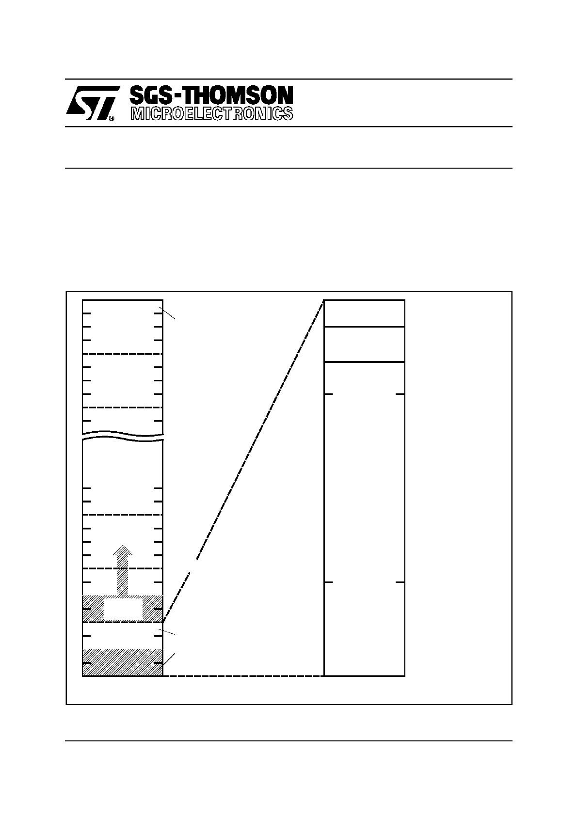
The ST10R163 provides a total addressable
memory space of 16 MBytes. This address space
is arranged as 256 segments of 64 KBytes each,
and each segment is again subdivided into four
data pages of 16 KBytes each (see figure below).
Figure 2-1. Memory Areas and Address
VR02081B
Segment
Segment
Segment
Segment
2
255
254
FF FFFFH
H
0000
FF
03 0000 H
H
0000
02
H
0000
01
H
0000
00
FE 0000 H
Data Page1023
0
Page
Data
Data Page3
RAM/SFR Area
Memory
External
FFFF
00
H
H
00 F000
H
00 C000
H
00 8000
H
00 4000
H
00 0000
Data Page0
1
Page
Data
Data Page2
3
Page
Data
Address Space
16 MByte
KByte
64
Segment
System
0
Segment
1
0
’
’
’
’
’
’
’
’
’
’
’
’
’
XSSP
’E000
00
H
19
2/8
2 - MEMORY ORGANIZATION (ST10R163)
Space
Most internal memory areas are mapped into seg-
ment 0, the system segment. The upper 4 KByte
of segment 0 (00’F000h...00’FFFFh) hold the In-
ternal RAM and Special Function Register Areas
(SFR and ESFR).
Code and data may be stored in any part of the in-
ternal memory areas, except for the SFR blocks,
which may be used for control / data, but not for in-
structions.
Note: The ST10R163 is a Romless device: pro-
gram ROM must be in external memory.
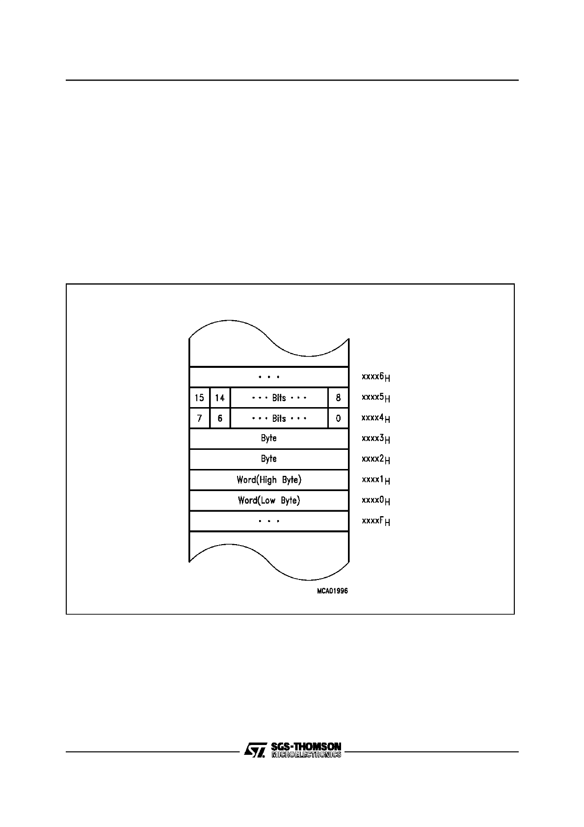
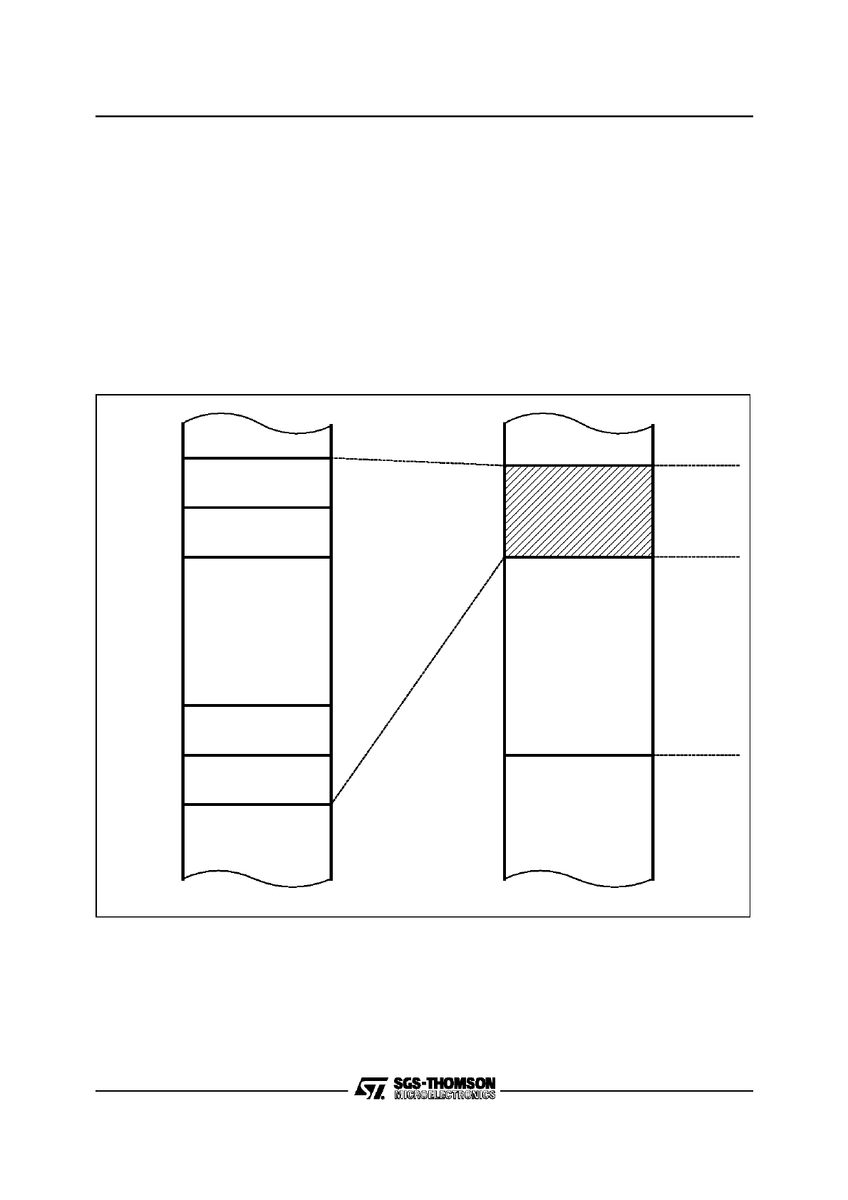
Bytes are stored at even or odd byte addresses.
Words are stored in ascending memory locations
with the low byte at an even byte address being
followed by the high byte at the next odd byte ad-
dress. Double words (code only) are stored in as-
cending memory locations as two subsequent
words. Single bits are always stored in the speci-
fied bit position at a word address. Bit position 0 is
the least significant bit of the byte at an even byte
address, and bit position 15 is the most significant
bit of the byte at the next odd byte address. Bit ad-
dressing is supported for a part of the Special
Function Registers, a part of the internal RAM and
for the General Purpose Registers.
Figure 2-2. Storage of Words, Byte and Bits in a Byte Organized Memory
Note: Byte units forming a single word or a double word must always be stored within the same physical (internal, exter-
nal, ROM, RAM) and organizational (page, segment) memory area.
20
3/8
2 - MEMORY ORGANIZATION (ST10R163)
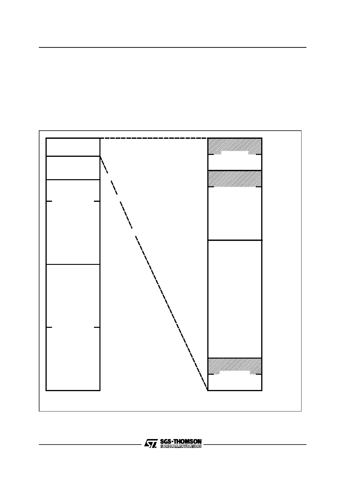
2.1 INTERNAL RAM AND SFR AREA
The RAM/SFR area is located within data page 3
and provides access to 1 KByte of on-chip RAM
(organized as 512*16) and to two 512 Byte blocks
of Special Function Registers (SFRs).
The internal RAM serves for several purposes:
– System Stack (programmable size)
– General Purpose Register Banks (GPRs)
– Source and destination pointers for the Periph-
eral Event Controller (PEC)
– Variable and other data storage, or
– Code storage.
Figure 2-3. Internal RAM Area and SFR Areas
Note: The upper 256 bytes of SFR area, ESFR area and internal RAM are bit-addressable (see shaded blocks in the
figure above).
VR02082B
RAM/SFR Area
Internal
ROM
Area
Memory
External
FFFF
00
H
H
00 F000
H
00 C000
H
00 8000
H
00 4000
H
00 0000
KByte
64
Segment
System
0
00
H
FFFF
FE00
00
H
FA00
00
H
F000
00
H
4 KByte
Internal
RAM
Reserved
ESFR Area
SFR Area
RAM/SFR Area
H
00 F200
’
’
’
’
’
’
’
’
’
’
’
0
Page
Data
Data Page 1
2
Page
Data
Data Page 3
H
00 EF00
’
XSSP
21

4/8
2 - MEMORY ORGANIZATION (ST10R163)
INTERNAL RAM AND SFR AREA(Cont’d)
Code accesses are always made on even byte ad-
dresses. The highest possible code storage loca-
tion in the internal RAM is either 00’FDFEh for sin-
gle word instructions or 00’FDFCh for double word
instructions. The respective location must contain
a branch instruction (unconditional), because se-
quential boundary crossing from internal RAM to
the SFR area is not supported and causes errone-
ous results.
Any word and byte data in the internal RAM can
be accessed via indirect or long 16-bit addressing
modes, if the selected DPP register points to data
page 3. Any word data access is made on an even
byte address. The highest possible word data
storage location in the internal RAM is 00’FDFEh.
For PEC data transfers, the internal RAM can be
accessed independent of the contents of the DPP
registers via the PEC source and destination
pointers.
The
upper
256 Byte of the internal
RAM
(00’FD00h through 00’FDFFh) and the GPRs of
the current bank are provided for single bit stor-
age, and thus they are bit addressable.
System Stack
The system stack may be defined within the inter-
nal RAM. The size of the system stack is control-
led by bitfield STKSZ in register SYSCON (see ta-
ble below).
For all system stack operations the on-chip RAM
is accessed via the Stack Pointer (SP) register.
The stack grows downward from higher towards
lower RAM address locations. Only word access-
es are supported to the system stack. A stack
overflow
(STKOV)
and
a
stack
underflow
(STKUN) register are provided to control the lower
and upper limits of the selected stack area. These
two stack boundary registers can be used not only
for protection against data destruction, but also al-
low to implement a circular stack with hardware
supported system stack flushing and filling (except
for the 1KByte stack option).
The technique of implementing this circular stack
is described in chapter “System Programming”.
<STKSZ>
Stack Size (Words)
Internal RAM Addresses (Words)
0 0 0 b
256
00’FBFEh...00’FA00h (Default after Reset)
0 0 1 b
128
00’FBFEh...00’FB00h
0 1 0 b
64
00’FBFEh...00’FB80h
0 1 1 b
32
00’FBFEh...00’FBC0h
1 0 0 b
---
Reserved. Do not use this combination.
1 0 1 b
---
Reserved. Do not use this combination.
1 1 0 b
---
Reserved. Do not use this combination.
1 1 1 b
512
00’FDFEh...00’FA00h (Note: No circular stack)
22

5/8
2 - MEMORY ORGANIZATION (ST10R163)
INTERNAL RAM AND SFR AREA(Cont’d)
General Purpose Registers
The General Purpose Registers (GPRs) use a
block of 16 consecutive words within the internal
RAM. The Context Pointer (CP) register deter-
mines the base address of the currently active
register bank. This register bank may consist of up
to 16 word GPRs (R0, R1, ..., R15) and/or of up to
16 byte GPRs (RL0, RH0, ..., RL7, RH7). The six-
teen byte GPRs are mapped onto the first eight
word GPRs (see table below).
In contrast to the system stack, a register bank
grows from lower towards higher address loca-
tions and occupies a maximum space of 32 bytes.
The GPRs are accessed via short 2-, 4- or 8-bit
addressing modes using the Context Pointer (CP)
register as base address (independent of the cur-
rent DPP register contents). Additionally, each bit
in the currently active register bank can be ac-
cessed individually.
The ST10R163 supports fast register bank (con-
text) switching. Multiple register banks can physi-
cally exist within the internal RAM at the same
time. Only the register bank selected by the Con-
text Pointer register (CP) is active at a given time,
however. Selecting a new active register bank is
simply done by updating the CP register. A partic-
ular Switch Context (SCXT) instruction performs
register bank switching and an automatic saving
of the previous context. The number of implement-
ed register banks (arbitrary sizes) is only limited
by the size of the available internal RAM.
Details on using, switching and overlapping regis-
ter banks are described in chapter “System Pro-
gramming”.
Mapping of General Purpose Registers to RAM Addresses
Internal RAM Address
Byte Registers
Word Register
<CP> + 1Eh
---
R15
<CP> + 1Ch
---
R14
<CP> + 1Ah
---
R13
<CP> + 18h
---
R12
<CP> + 16h
---
R11
<CP> + 14h
---
R10
<CP> + 12h
---
R9
<CP> + 10h
---
R8
<CP> + 0Eh
RH7RL7
R7
<CP> + 0Ch
RH6RL6
R6
<CP> + 0Ah
RH5RL5
R5
<CP> + 08h
RH4RL4
R4
<CP> + 06h
RH3RL3
R3
<CP> + 04h
RH2RL2
R2
<CP> + 02h
RH1RL1
R1
<CP> + 00h
RH0RL0
R0
23
6/8
2 - MEMORY ORGANIZATION (ST10R163)
INTERNAL RAM AND SFR AREA(Cont’d)
PEC Source and Destination Pointers
The 16 word locations in the internal RAM from
00’FCE0h to 00’FCFEh (just below the bit-ad-
dressable section) are provided as source and
destination address pointers for data transfers on
the eight PEC channels. Each channel uses a pair
of pointers stored in two subsequent word loca-
tions with the source pointer (SRCPx) on the lower
and the destination pointer (DSTPx) on the higher
word address (x = 7...0).
Whenever a PEC data transfer is performed, the
pair of source and destination pointers, which is
selected by the specified PEC channel number, is
accessed independent of the current DPP register
contents and also the locations referred to by
these pointers are accessed independent of the
current DPP register contents. If a PEC channel is
not used, the corresponding pointer locations area
available and can be used for word or byte data
storage.
For more details about the use of the source and
destination pointers for PEC data transfers see
section “Interrupt and Trap Functions”.
Figure 2-4. Location of the PEC Pointers
VR02083B
DSTP7
SRCP7
PEC
Source
and
Destination
Pointers
DSTP0
SRCP0
Internal
RAM
00’FCFE
00’FCFC
00’FCE2
00’FCE0
00’F9FE
00’FA00
00’FCE0
00’FCFE
00’FD00
00’FDDE
H
H
H
H
H
H
H
H
H
H
24

7/8
2 - MEMORY ORGANIZATION (ST10R163)
INTERNAL RAM AND SFR AREA(Cont’d)
Special Function Registers
The functions of the CPU, the bus interface, the IO
ports
and
the
on-chip
peripherals
of
the
ST10R163 are controlled via a number of Special
Function Registers (SFRs). These SFRs are ar-
ranged within two areas of 512 Byte size each.
The first register block, the SFR area, is located in
the
512
Bytes
above
the
internal
RAM
(00’FFFFh...00’FE00h), the second register block,
the Extended SFR (ESFR) area, is located in the
512
Bytes
below
the
internal
RAM
(00’F1FFh...00’F000h).
Special function registers can be addressed via in-
direct and long 16-bit addressing modes. Using an
8-bit offset together with an implicit base address
allows to address word SFRs and their respective
low bytes. However, thisdoes not work for the re-
spective high bytes!
Note: Writing to any byte of an SFR causes the
non-addressed
complementary
byte
to
be
cleared!
The upper half of each register block is bit-ad-
dressable, so the respective control/status bits
can directly be modified or checked using bit ad-
dressing.
When accessing registers in the ESFR area using
8-bit addresses or direct bit addressing, an Extend
Register (EXTR) instruction is required before, to
switch the short addressing mechanism from the
standard SFR area to the Extended SFR area.
This is not required for 16-bit and indirect address-
es. The GPRs R15...R0 are duplicated, ie. they
are accessible within both register blocks via short
2-, 4- or 8-bit addresses without switching.
Example:
EXTR
#4
;Switc h to ESFR area for the next 4
instru ctions
MOV
ODP2, #dat a16
;ODP2 uses 8-bit reg addres sing
BFLDL
DP6, #mas k, #data8
;Bit addr essing for bit fiel ds
BSET
DP1H.7
;Bit addr essing for single bits
MOV
T8REL, R1
;T8REL uses 16-bi t address , R1 is
duplic ated...
;...an d also accessible via the ESFR
mode
;(EXTR is not require d for this
access )
;----- -- ;-------- ---- ---- ---
;The scope of the EXTR #4 inst ruct ion
ends here !
MOV
T8REL, R1
;T8REL uses 16-bi t address , R1 is
duplic ated...
;...an d does not requi re switchi ng
In order to minimize the use of the EXTR instruc-
tions the ESFR area mostly holds registers which
are mainly required for initialization and mode se-
lection. Registers that need to be accessed fre-
quently are allocated to the standard SFR area,
wherever possible.
Note: The development tools are equipped to
monitor accesses to the ESFR area and will auto-
matically insert EXTR instructions, or issue a
warning in case of missing or excessive EXTR in-
structions.
25

8/8
2 - MEMORY ORGANIZATION (ST10R163)
2.2 EXTERNAL MEMORY SPACE
The ST10R163 is capable of using an address
space of up to 16 MByte. Only parts of this ad-
dress space are occupied by internal memory are-
as. All addresses which are not used for on-chip
RAM, for registers or internal Xperipherals may
reference external memory locations. This exter-
nal memory is accessed via the ST10R163’s ex-
ternal bus interface.
Four memory bank sizes are supported:
– Non-segmented mode: 64KByte with A15...A0
on PORT0 or PORT1
– 2- bit segmented mode: 256 KByte with
A17...A16 on Port 4 and A15...A0 on PORT0 or
PORT1
– 4-bit segmented mode: 1 MByte with A19...A16
on Port 4 and A15...A0 on PORT0 or PORT1
– 8-bit segmented mode: 16 MByte with A23...A16
on Port 4 and A15...A0 on PORT0 or PORT1
Each bank can be directly addressed via the ad-
dress bus, while the programmable chip select
signals can be used to select various memory
banks.
The ST10R163 also supports four different bus
types:
– Multiplexed 16-bit Bus, with address and data on
PORT0 (Default after Reset)
– Multiplexed 8-bit Bus, with address and data on
PORT0/P0L
– Demultiplexed 16-bit Bus, with address on
PORT1 and data on PORT0
– Demultiplexed 8-bit Bus, with address on
PORT1 and data on P0L
Memory model and bus mode are selected during
reset by pin EA and PORT0 pins. For further de-
tails about the external bus configuration and con-
trol please refer to chapter ”The External Bus In-
terface”.
External word and byte data can only be accessed
via indirect or long 16-bit addressing modes using
one of the four DPP registers. There is no short
addressing mode for external operands. Any word
data access is made to an even byte address.
For PEC data transfers the external memory in
segment 0 can be accessed independent of the
contents of the DPP registers via the PEC source
and destination pointers.
The external memory is not provided for single bit
storage and therefore it is not bit addressable.
2.3 CROSSING MEMORY BOUNDARIES
The address space of the ST10R163 is implicitly
divided into equally sized blocks of different gran-
ularity and into logical memory areas. Crossing
the boundaries between these blocks (code or da-
ta) or areas requires special attention to ensure
that the controller executes the desired opera-
tions.
Memory Areas are partitions of the address
space that represent different kinds of memory (if
provided at all). These memory areas are the in-
ternal RAM/SFR area, and the external memory.
Accessing subsequent data locations that belong
to different memory areas is no problem. Howev-
er, when executing code, the different memory ar-
eas must be switched explicitly via branch instruc-
tions. Sequential boundary crossing is not sup-
ported and leads to erroneous results.
Note: Changing from the external memory area to
the internal RAM/SFR area takes place within
segment 0.
Segments are contiguous blocks of 64 KByte
each. They are referenced via the code segment
pointer CSP for code fetches and via an explicit
segment number for data accesses overriding the
standard DPP scheme.
During code fetching segments are not changed
automatically, but rather must be switched explic-
itly. The instructions JMPS, CALLS and RETS will
do this.
In larger sequential programs make sure that the
highest used code location of a segment contains
an unconditional branch instruction to the respec-
tive following segment, to prevent the prefetcher
from trying to leave the current segment.
Data Pages are contiguous blocks of 16 KByte
each. They are referenced via the data page
pointers DPP3...0 and via an explicit data page
number for data accesses overriding the standard
DPP scheme. Each DPP register can select one
of the possible 1024 data pages. The DPP register
that is used for the current access is selected via
the two upper bits of the 16-bit data address. Sub-
sequent 16-bit data addresses that cross the 16
KByte data page boundaries therefore will use dif-
ferent data page pointers, while the physical loca-
tions need not be subsequent within memory.
26
February 1996
1/26
This is advance information from SGS-TH OMSON. Details are subject tochange without notice.
ST10R163
User Manual
3 - CENTRAL PROCESSING UNIT
Basic tasks of the CPU are to fetch and decode in-
structions, to supply operands for the arithmetic
and logic unit (ALU), to perform operations on
these operands in the ALU, and to store the previ-
ously calculated results. As the CPU is the main
engine of the ST10R163 controller, it is also af-
fected by certain actions of the peripheral subsys-
tem.
Since a four stage pipeline is implemented in the
ST10R163, up to four instructions can be proc-
essed
in
parallel.
Most instructions
of the
ST10R163 are executed in one machine cycle (ie.
100 ns @ 20 MHz CPU clock) due to this parallel-
ism. This chapter describes how the pipeline
works for sequential and branch instructions in
general, and which hardware provisions have
been made to speed the execution of jump in-
structions in particular. The general instruction
timing is described including standard and excep-
tional timing.
While internal memory accesses are normally per-
formed by the CPU itself, external peripheral or
memory accesses are performed by a particular
on-chip External Bus Controller (EBC), which is
automatically invoked by the CPU whenever a
code or data address refers to the external ad-
dress space. If possible, the CPU continues oper-
ating while an external memory access is in
progress. If external data are required but are not
yet available, or if a new external memory access
is requested by the CPU, before a previous ac-
cess has been completed, the CPU will be held by
the EBC until the request can be satisfied. The
EBC is described in a dedicated chapter.
Figure 3-1. CPU Block Diagram
VR02080B
CPU
SP
STKOV
STKUN
Instr.Reg.
Instr.Ptr.
Exec.Unit
4-Stage
Pipeline
MDH
MDL
PSW
SYSCON
Context Ptr.
Mul/Div-HW
Gen
-
R15
R0
General
Purpose
Registers
Bit-Mask
Barrel Shifter
ALU
(16-bit)
Data Page Ptr.
CodeSeg. Ptr.
RAM
R15
R0
ROM
16
16
32
BUSCON 0
BUSCON 1
BUSCON 2
BUSCON 3
BUSCON 4
ADDRSEL 4
ADDRSEL 3
ADDRSEL 2
ADDRSEL 1
1 KByte
27

2/26
3 - CENTRAL PROCESSING UNIT (ST10R163)
The on-chip peripheral units of the ST10R163
work nearly independently of the CPU with a sep-
arate clock generator. Data and control informa-
tion is interchanged between the CPU and these
peripherals
via
Special
Function
Registers
(SFRs). Whenever peripherals need a non-deter-
ministic CPU action, an on-chip Interrupt Control-
ler compares all pending peripheral service re-
quests against each other and prioritizes one of
them. If the priority of the current CPU operation is
lower than the priority of the selected peripheral
request, an interrupt will occur.
Basically, there are two types of interrupt process-
ing:
•
Standard interrupt processingforces the CPU
to save the current program status and the return
address on the stack before branching to the inter-
rupt vector jump table.
•
PEC interrupt processing steals just one ma-
chine cycle from the current CPU activity to per-
form a single data transfer via the on-chip Periph-
eral Event Controller (PEC).
System errors detected during program execution
(hardware traps) or an external non-maskable in-
terrupt are also processed as standard interrupts
with a very high priority.
In contrast to other on-chip peripherals, there is a
closer conjunction between the watchdog timer
and the CPU. If enabled, the watchdog timer ex-
pects to be serviced by the CPU within a program-
mable period of time, otherwise it will reset the
chip. Thus, the watchdog timer is able to prevent
the CPU from going totally astray when executing
erroneous code. After reset, the watchdog timer
starts counting automatically, but it can be disa-
bled via software, if desired.
Beside its normal operation there are the following
particular CPU states:
•
Reset state: Any reset (hardware, software,
watchdog) forces the CPU into a predefined active
state.
•
IDLE state: The clock signal to the CPU itself is
switched off, while the clocks for the on-chip pe-
ripherals keep running.
•
POWER DOWN state: All of the on-chip clocks
are switched off.
A transition into an active CPU state is forced by
an interrupt (if being IDLE) or by a reset (if being in
POWER DOWN mode).
The IDLE, POWER DOWN and RESET states
can be entered by particular ST10R163 system
control instructions.
A set of Special Function Registers is dedicated to
the functions of the CPU core:
•
General
System
Configuration:
SYSCON
(RP0H)
•
CPU Status Indication and Control: PSW
•
Code Access Control: IP, CSP
•
Data Paging Control: DPP0, DPP1, DPP2,
DPP3
•
GPRs Access Control: CP
•
System Stack Access Control: SP, STKUN,
STKOV
•
Multiply and Divide Support: MDL, MDH, MDC
•
ALU Constants Support: ZEROS, ONES
3.1 INSTRUCTION PIPELINING
The instruction pipeline of the ST10R163 parti-
tiones instruction processing into four stages of
which each one has its individual task:
1st –>FETCH:
In this stage the instruction selected by the In-
struction Pointer (IP) and the Code Segment
Pointer (CSP) is fetched from either the internal
RAM or external memory.
2nd –>DECODE:
In this stage the instructions are decoded and, if
required, the operand addresses are calculated
and the respective operands are fetched. For all
instructions, which implicitly access the system
stack, the SP register is either decremented or in-
cremented, as specified. For branch instructions
the Instruction Pointer and the Code Segment
Pointer are updated with the desired branch target
address (provided that the branch is taken).
3rd –>EXECUTE:
In this stage an operation is performed on the pre-
viously fetched operands in the ALU. Additionally,
the condition flags in the PSW register are updat-
ed as specified by the instruction. All explicit writes
to the SFR memory space and all auto-increment
or auto-decrement writes to GPRs used as indi-
rect address pointers are performed during the ex-
ecute stage of an instruction, too.
4th –>WRITE BACK:
In this stage all external operands and the remain-
ing operands within the internal RAM space are
written back.
A particularity of the ST10R163 are the injected in-
structions. These injected instructions are gener-
ated internally by the machine to provide the time
needed to process instructions, which cannot be
processed within one machine cycle. They are au-
tomatically injected into the decode stage of the
pipeline, and then they pass through the remain-
ing stages like every standard instruction. Pro-
gram interrupts are performed by means of inject-
ed instructions, too. Although these internally in-
jected instructions will not be noticed in reality,
they are introduced here to ease the explanation
of the pipeline in the following.
28
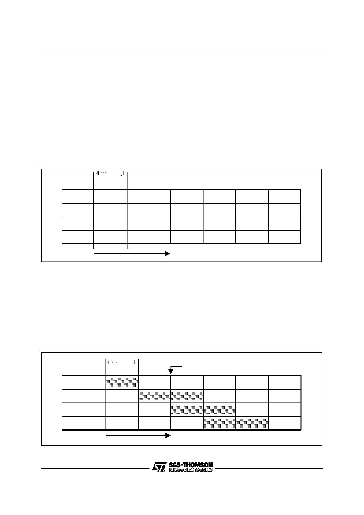
3/26
3 - CENTRAL PROCESSING UNIT (ST10R163)
INSTRUCTION PIPELINING (Cont’d)
Sequential Instruction Processing
Each single instruction has to pass through each
of the four pipeline stages regardless of whether
all possible stage operations are really performed
or not. Since passing through one pipeline stage
takes at least one machine cycle, any isolated in-
struction takes at least four machine cycles to be
completed. Pipelining, however, allows parallel
(ie. simultaneous) processing of up to four instruc-
tions. Thus, most of the instructions seem to be
processed during one machine cycle as soon as
the pipeline has been filled once after reset (see
figure below).
Instruction pipelining increases the average in-
struction throughput considered over a certain pe-
riod of time. In the following, any execution time
specification of an instruction always refers to the
average execution time due to pipelined parallel
instruction processing.
Figure 3-2. Sequential Instruction Pipelining
Standard Branch Instruction Processing
Instruction pipelining helps to speed sequential
program processing. In the case that a branch is
taken, the instruction which has already been
fetched providently is mostly not the instruction
which must be decoded next. Thus, at least one
additional machine cycle is normally required to
fetch the branch target instruction. This extra ma-
chine cycle is provided by means of an injected in-
struction (see figure below).
If a conditional branch is not taken, there is no de-
viation from the sequential program flow, and thus
no extra time is required. In this case the instruc-
tion after the branch instruction will enter the de-
code stage of the pipeline at the beginning of the
next machine cycle after decode of the conditional
branch instruction.
Figure 3-3. Standard Branch Instruction Pipelining
1 Machine
Cycle
FETCH
I
2
I
1
I
3
I
2
I
1
I
4
I
3
I
2
I
1
I
6
I
5
I
4
I
3
I
5
I
4
I
3
I
2
I
1
DECODE
EXECUTE
WRITEBACK
time
1 Machine
Cycle
FETCH
I
n+2
BRANCH
I
n
. . .
I
TARGET
(I
INJECT
)
BRANCH
I
n
I
TARGET+1
I
TARGET
(I
INJECT
)
BRANCH
I
TARGET+3
I
TARGET+2
I
TARGET+1
I
TARGET
I
TARGET+2
I
TARGET+1
I
TARGET
(I
INJECT
)
BRANCH
I
n
. . .
. . .
DECODE
EXECUTE
WRITEBACK
time
Injection
29
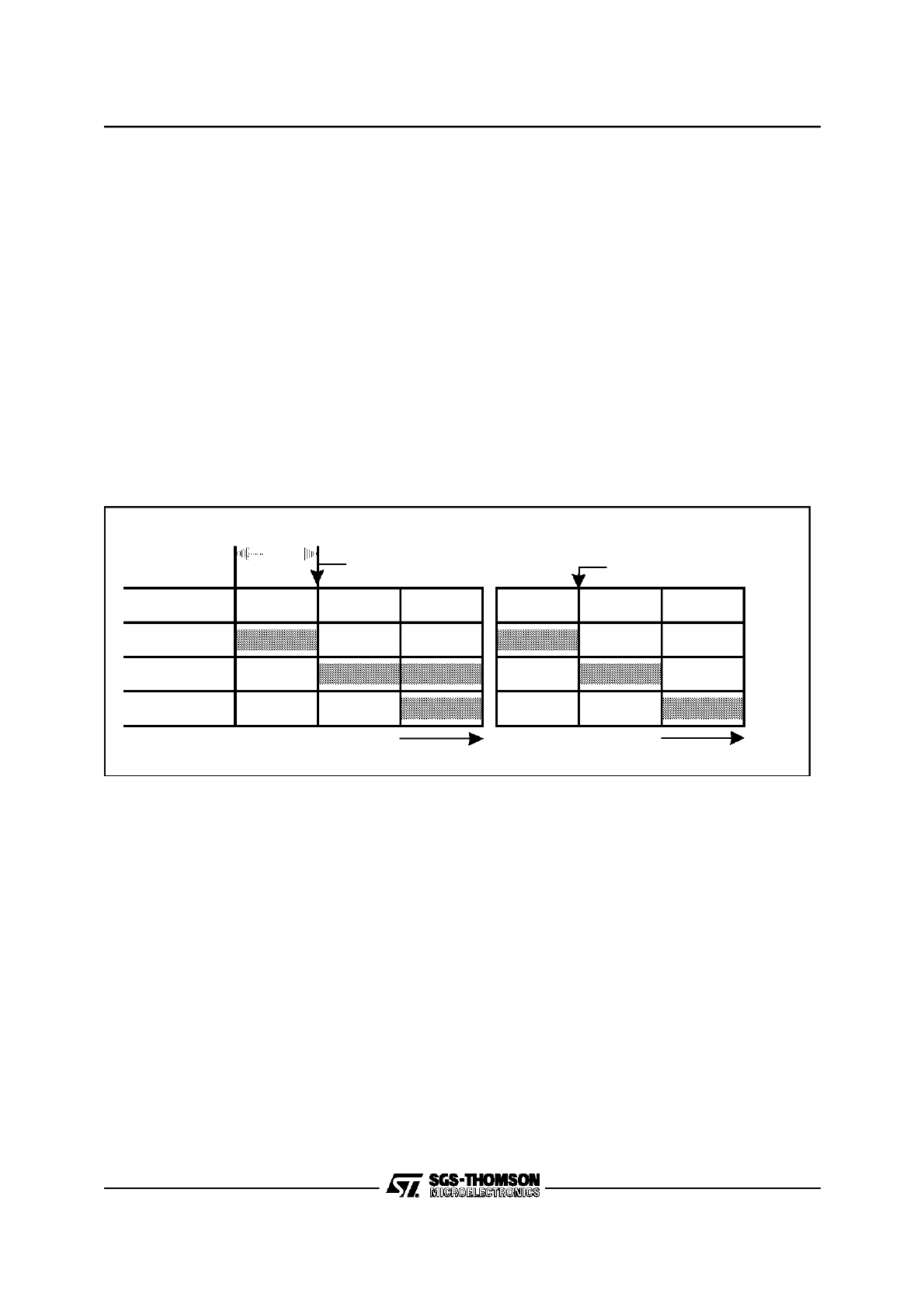
4/26
3 - CENTRAL PROCESSING UNIT (ST10R163)
INSTRUCTION PIPELINING (Cont’d)
Cache Jump Instruction Processing
The ST10R163 incorporates a jump cache to opti-
mize conditional jumps, which are processed re-
peatedly within a loop. Whenever a jump on cache
is taken, the extra time to fetch the branch target
instruction can be saved and thus the correspond-
ing cache jump instruction in most cases takes
only one machine cycle.
This performance is achieved by the following
mechanism:
Whenever a cache jump instruction passes
through the decode stage of the pipeline for the
first time (and provided that the jump condition is
met), the jump target instruction is fetched as usu-
al, causing a time delay of one machine cycle. In
contrast to standard branch instructions, however,
the target instruction of a cache jump instruction
(JMPA, JMPR, JB, JBC, JNB, JNBS) is additional-
ly stored in the cache after having been fetched.
After each repeatedly following execution of the
same cache jump instruction, the jump target in-
struction is not fetched from progam memory but
taken from the cache and immediatly injected into
the decode stage of the pipeline (see figure be-
low).
A time saving jump on cache is always taken after
the second and any further occurrence of the
same cache jump instruction, unless an instruc-
tion which, has the fundamental capability of
changing the CSP register contents (JMPS,
CALLS, RETS, TRAP, RETI), or any standard in-
terrupt has been processed during the period of
time between two following occurrences of the
same cache jump instruction.
Figure 3-4. Cache Jump Instruction Pipelining
I
n+2
Cache Jmp
I
n
. . .
I
TARGET+1
I
TARGET
Cache Jmp
I
n
I
TARGET+2
I
TARGET+1
I
TARGET
Cache Jmp
I
n+2
Cache Jmp
I
n
. . .
I
TARGET
(I
INJECT
)
Cache Jmp
I
n
I
TARGET+1
I
TARGET
(I
INJECT
)
Cache Jmp
1 Machine
Cycle
FETCH
DECODE
EXECUTE
WRITEBACK
1st loop iteration
Injection
Injection of cached
Target Instruction
Repeated loop iteration
30

5/26
3 - CENTRAL PROCESSING UNIT (ST10R163)
INSTRUCTION PIPELINING (Cont’d)
Particular Pipeline Effects
Since up to four different instructions are proc-
essed simultaneously, additional hardware has
been spent in the ST10R163 to consider all causal
dependencies which may exist on instructions in
different pipeline stages without a loss of perform-
ance. This extra hardware (ie. for ’forwarding’ op-
erand read and write values) resolves most of the
possible conflicts (eg. multiple usage of buses) in
a time optimized way and thus avoids that the
pipeline becomes noticeable for the user in most
cases. However, there are some very rare cases,
where the circumstance that the ST10R163 is a
pipelined machine requires attention by the pro-
grammer. In these cases the delays caused by
pipeline conflicts can be used for other instruc-
tions in order to optimize performance.
n Context Pointer Updating
An instruction, which calculates a physical GPR
operand address via the CP register, is mostly not
capable of using a new CP value, which is to be
updated by an immediately preceding instruction.
Thus, to make sure that the new CP value is used,
at least one instruction must be inserted between
a CP-changing and a subsequent GPR-using in-
struction, as shown in the following example:
In:
SCXT
CP, #0FC 00h;
;selec t a new contex t
I
n+1
:
....
;must not be an inst ruct ion using
;a GPR
I
n+2
:
MOV
R0, #dataX
;write to GPR 0 in the new context
n Data Page Pointer Updating
An instruction, which calculates a physical oper-
and address via a particular DPPn (n=0 to 3) reg-
ister, is mostly not capable of using a new DPPn
register value, which is to be updated by an imme-
diately preceding instruction. Thus, to make sure
that the new DPPn register value is used, at least
one instruction must be inserted between a DPPn-
changing instruction and a subsequent instruction
which implicitly uses DPPn via a long or indirect
addressing mode, as shown in the following ex-
ample:
I
n
:
MOV
DPP0, #4
;selec t data page 4 via DPP0
I
n+1
:
....
;must not be an instructi on using DPP0
I
n+2
:
MOV
DPP0: 0000h, R1
;move
cont ents
of
R1
to
address
;locat ion 01’000 0h (in
data
page
4)
;suppo sed segment atio n is enabled
n Explicit Stack Pointer Updating
None of the RET, RETI, RETS, RETP or POP in-
structions is capable of correctly using a new SP
register value, which is to be updated by an imme-
diately preceding instruction. Thus, in order to use
the new SP register value without erroneously
performed stack accesses, at least one instruction
must be inserted between an explicitly SP-writing
and any subsequent of the just mentioned implic-
itly SP-using instructions, as shown in the follow-
ing example:
I
n
:
MOV
SP, #0FA4 0h
;selec t a new top of stack
I
n+1
:
....
;must
not
be an
instruc tion popp ing
;opera nds from the syst em stack
I
n+2
:
POP
R0
;pop word value from new top of stack
;into R0
n External Memory Access Sequences
The effect described here will only become notice-
able, when watching the external memory access
sequences on the external bus (eg. by means of a
Logic Analyzer). Different pipeline stages can si-
multaneously put a request on the External Bus
Controller (EBC). The sequence of instructions
processed by the CPU may diverge from the se-
quence of the corresponding external memory ac-
cesses performed by the EBC, due to the prede-
fined priority of external memory accesses:
1st
Write Data
2nd Fetch Code
3rd
Read Data.
31

6/26
3 - CENTRAL PROCESSING UNIT (ST10R163)
INSTRUCTION PIPELINING (Cont’d)
n Controlling Interrupts
Software modifications (implicit or explicit) of the
PSW are done in the execute phase of the respec-
tive instructions. In order to maintain fast interrupt
responses, however, the current interrupt prioriti-
zation round does not consider these changes, ie.
an interrupt request may be acknowledged after
the instruction that disables interrupts via IEN or
ILVL or after the following instructions. Time criti-
cal instruction sequences therefore should not be-
gin directly after the instruction disabling inter-
rupts, as shown in the following example:
INT_OF F:
BCLR
IEN
;globa lly disable inte rrupts
I
N-1
;non-c ritica l instr uction
CRIT_1 ST :
I
N
;begin
of
unin terr uptable
crit ical
;seque nce
. . .
CRIT_L AST:
I
N+x
;end
of
unint erru ptab le
critical
;seque nce
INT_ON :
BSET
IEN
;globa lly re-enabl e interr upts
Note: The described delay of 1 instruction also ap-
plies for enabling the interrupts system ie. no inter-
rupt requests are acknowledged until the instruc-
tion following the enabling instruction.
n Initialization of Port Pins
Modifications of the direction of port pins (input or
output) become effective only after the instruction
following the modifying instruction. As bit instruc-
tions (BSET, BCLR) use internal read-modify-
write sequences accessing the whole port, in-
structions modifying the port direction should be
followed by an instruction that does not access the
same port (see example below).
WRONG:
BSET
DP3.13;
;chang e direct ion of P3.13 to output
BSET
P3.5
;
;P3.13 is still input , the rd-mod -wr
;reads pin P3.13
RIGHT:
BSET
DP3.13;
;chang e direct ion of P3.13 to output
NOP
;any instr ucti on not accessing port 3
BSET
P3.5
;
;P3.13 is now output, the rd-mod-wr
;reads the P3.13 output latch
n Changing the System Configuration
The instruction following an instruction that chang-
es the system configuration via register SYSCON
(eg.
segmentation, stack size) cannot use the
new resources (eg. stack). In these cases an in-
struction that does not access these resources
should be inserted.
n BUSCON/ADDRSEL
The instruction following an instruction that chang-
es the properties of an external address area can-
not access operands within the new area. In these
cases an instruction that does not access this ad-
dress area should be inserted. Code accesses to
the new address area should be made after an ab-
solute branch to this area.
Note: As a rule, instructions that change external
bus properties should not be executed from the re-
spective external memory area.
n Updating the Stack Pointer
An instruction that changes the contents of the
stack pointer SP (MOV, ADD, SUB) may not be
followed directly by an instruction that implicitly
uses the SP, ie. a POP or RETURN instruction. To
ensure proper operation an instruction should be
inserted that does not use the stack pointer.
n Timing
Instruction pipelining reduces the average instruc-
tion processing time in a wide scale (from four to
one machine cycles, mostly). However, there are
some rare cases, where a particular pipeline situ-
ation causes the processing time for a single in-
struction to be extended either by a half or by one
machine cycle. Although this additional time rep-
resents only a tiny part of the total program execu-
tion time, it might be of interest to avoid these
pipeline-caused time delays in time critical pro-
gram modules.
Besides a general execution time description, the
following section provides some hints on how to
optimize time-critical program parts with regard to
such pipeline-caused timing particularities.
32

7/26
3 - CENTRAL PROCESSING UNIT (ST10R163)
3.2 BIT-HANDLING AND BIT-PROTECTION
The ST10R163 provides several mechanisms to
manipulate bits. These mechanisms either manip-
ulate software flags within the internal RAM, con-
trol on-chip peripherals via control bits in their re-
spective SFRs or control IO functions via port
pins.
The instructions BSET, BCLR, BAND, BOR, BX-
OR, BMOV, BMOVN explicitly set or clear specific
bits. The instructions BFLDL and BFLDH allow to
manipulate up to 8 bits of a specific byte at one
time. The instructions JBC and JNBS implicitly
clear or set the specified bit when the jump is tak-
en. The instructions JB and JNB (also conditional
jump instructions that refer to flags) evaluate the
specified bit to determine if the jump is to be taken.
Note: Bit operations on undefined bit locations will
always read a bit value of ‘0’, while the write ac-
cess will not affect the respective bit location.
All instructions that manipulate single bits or bit
groups internally use a read-modify-write se-
quence that accesses the whole word, which con-
tains the specified bit(s).
This method has several consequences:
•
Bits can only be modified within the internal ad-
dress areas, ie. internal RAM and SFRs. External
locations cannot be used with bit instructions.
The upper 256 bytes of the SFR area, the ESFR
area and the internal RAM are bit-addressable
(see chapter “Memory Organization”), ie. those
register bits located within the respective sections
can be directly manipulated using bit instructions.
The other SFRs must be accessed byte/word
wise.
Note: All GPRs are bit-addressable independent
of the allocation of the register bank via the con-
text pointer CP. Even GPRs which are allocated to
not bit-addressable RAM locations provide this
feature.
•
The read-modify-write approach may be critical
with hardware-effected bits. In these cases the
hardware may change specific bits while the read-
modify-write operation is in progress, where the
writeback would overwrite the new bit value gen-
erated by the hardware. The solution is either the
implemented hardware protection (see below) or
realized through special programming (see “Par-
ticular Pipeline Effects”).
Protected bits are not changed during the read-
modify-write sequence, ie. when hardware sets
eg. an interrupt request flag between the read and
the write of the read-modify-write sequence. The
hardware protection logic guarantees that only the
intended bit(s) is/are affected by the write-back
operation.
Note: If a conflict occurs between a bit manipula-
tion generated by hardware and an intended soft-
ware access the software access has priority and
determines the final value of the respective bit.
A summary of the protected bits implemented in
the ST10R163 can be found at the end of chapter
“Architectural Overview”.
33

8/26
3 - CENTRAL PROCESSING UNIT (ST10R163)
3.3 INSTRUCTION STATE TIMES
Basically, the time to execute an instruction de-
pends on where the instruction is fetched from,
and where possible operands are read from or
written to. The fastest processing mode of the
ST10R163 is to execute a program fetched from
fast external memory (no wait states), using a 16-
bit demultiplexed bus. In that case most of the in-
structions can be processed within just one ma-
chine cycle, which is also the general minimum
execution time.
All external memory accesses are performed by
the ST10R163’s on-chip External Bus Controller
(EBC), which works in parallel with the CPU.
This section summarizes the execution times in a
very condensed way. A detailled description of the
execution times for the various instructions and
the specific exceptions can be found in the“ST10
Family Programming Manual”.
The table below shows the minimum execution
times required to process a ST10R163 instruction
fetched from the internal RAM or from external
memory. These execution times apply to most of
the ST10R163 instructions - except some of the
branches, the multiplication and the division in-
structions and a special move instruction. The
numbers in the table are in units of [ns], refer to a
CPU clock of 20 MHz and assume no waitstates.
Execution from the internal RAM provides flexibili-
ty in terms of loadable and modifiable code on the
account of execution time.
Execution from external memory strongly de-
pends on the selected bus mode and the program-
ming of the bus cycles (waitstates).
The operand and instruction accesses listed be-
low can extend the execution time of an instruc-
tion:
– Internal RAM operand reads via indirect ad-
dressing modes
– Internal SFR operand reads immediately after
writing
– External operand reads
– External operand writes
– Testing Branch Conditions immediately after
PSW writes
Minimum Execution Times
Instruction Fetch
Word Operand Access
Memory Area
Word Instruction
Doublew ord
Instruction
Read from
Write to
Internal RAM
300
400
0/50
0
16-bit Demux Bus
100
200
100
100
16-bit Mux Bus
150
300
150
150
8-bit Demux Bus
200
400
200
200
8-bit Mux Bus
300
600
300
300
34
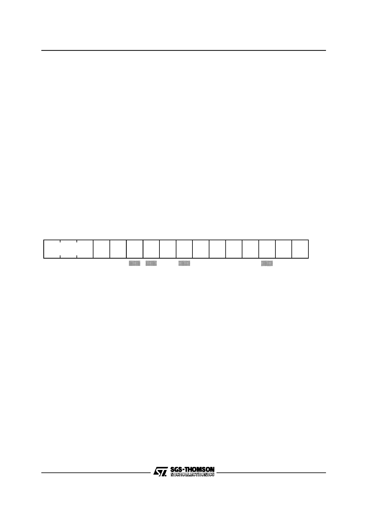
9/26
3 - CENTRAL PROCESSING UNIT (ST10R163)
3.4 CPU SPECIAL FUNCTION REGISTERS
The core CPU requires a set of Special Function
Registers (SFRs) to maintain the system state in-
formation, to supply the ALU with register-ad-
dressable constants and to control system and
bus configuration, multiply and divide ALU opera-
tions, code memory segmentation, data memory
paging, and accesses to the General Purpose
Registers and the System Stack.
The access mechanism for these SFRs in the
CPU core is identical to the access mechanism for
any other SFR. Since all SFRs can simply be con-
trolled by means of any instruction, which is capa-
ble of addressing the SFR memory space, a lot of
flexibility has been gained, without the need to
create a set of system-specific instructions.
Note, however, that there are user access restric-
tions for some of the CPU core SFRs to ensure
proper processor operations. The instruction
pointer IP and code segment pointer CSP cannot
be accessed directly at all. They can only be
changed indirectly via branch instructions.
The PSW, SP, and MDC registers can be modified
not only explicitly by the programmer, but also im-
plicitly by the CPU during normal instruction
processing. Note that any explicit write request
(via software) to an SFR supersedes a simultane-
ous modification by hardware of the same regis-
ter.
Note: Any write operation to a single byte of an
SFR clears the non-addressed complementary
byte within the specified SFR.
Non-implemented (reserved) SFR bits cannot be
modified, and will always supply a read value of
’0’.
The System Configuration Register SYSCON
This bit-addressable register provides general
system configuration and control functions. The
reset value for register SYSCON depends on the
state of the PORT0 pins during reset.
SYSCON (FF12h / 89h)
SFR
Reset Value: 0XX0h
XPER-
SHARE
VISI
BLE
-
-
-
-
SSP
EN
ROM
S1
WR
CFG
5
4
3
2
1
0
11
10
9
8
7
6
15
14
13
12
-
-
rw
rw
rw
rw
rw
rw
STKSZ
SGT
DIS
ROM
EN
rw
BYT
DIS
CLK
EN
rw
-
rw
-
rw
35
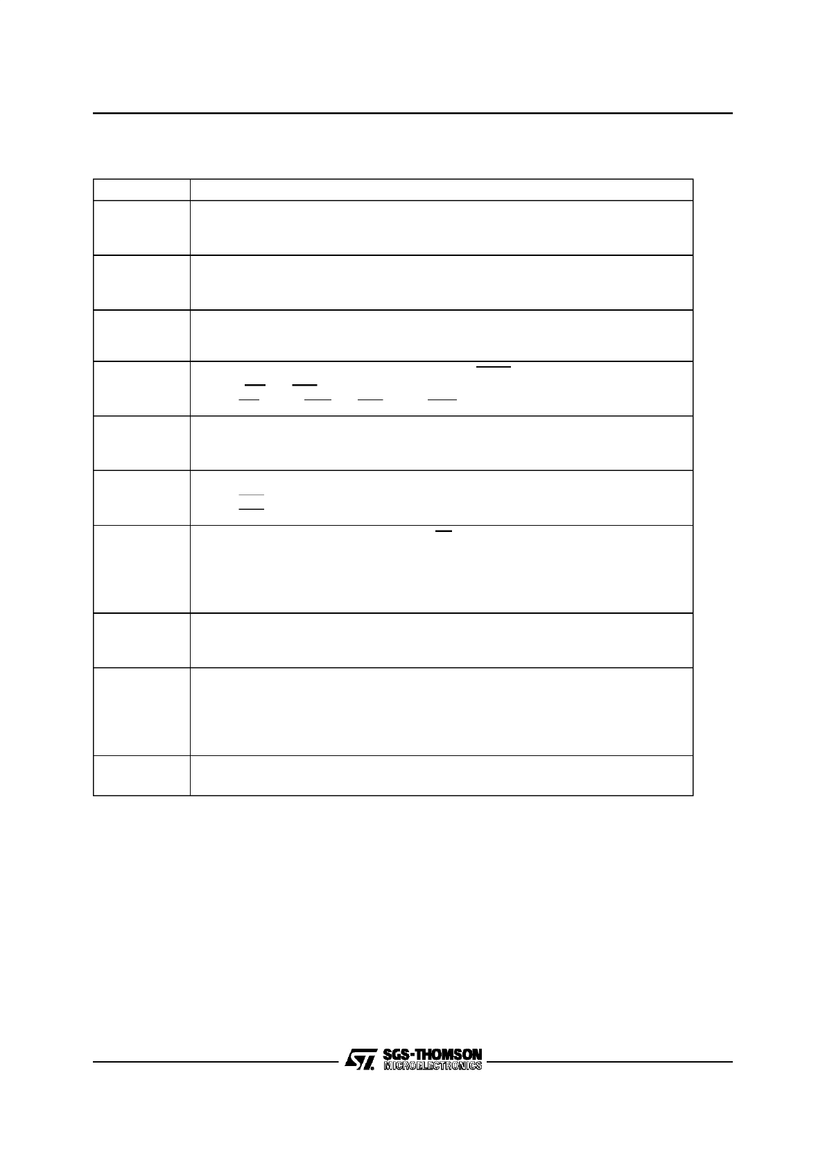
10/26
3 - CENTRAL PROCESSING UNIT (ST10R163)
CPU SPECIAL FUNCTION REGISTERS(Cont’d)
Note: Register SYSCON cannot be changed after execution of the EINIT instruction.
The function of bits XPER-SHARE, VISIBLE, WRCFG, BYTDIS, ROMEN and ROMS1 is described in more detail
in chapter “The External Bus Controller”.
Bit
Fun ction
XPER-SHARE
XBUS Peripheral Share Mode Control
‘0’: External accesses to XBUS peripherals are disabled
‘1’: XBUS peripherals are accessible via the external bus during hold mode.
VISIBLE
Visible Mode Control
‘0’: Accesses to XBUS peripherals are done internally
‘1’: XBUS peripheral accesses are made visible on the external pins.
SSPEN
Xperipheral SSP Enable Control
‘0’: SSP is disabled. Pins P4.[7..4] are general purpose IOs or segment address lines
‘1’: SSP is enabled. Pins P4.[7..4] are SSP IOs or segment address lines
WRCFG
Write Config uration Control (Set according to pin P0H.0 during reset)
‘0’: Pins WR and BHE retain their normal function
‘1’: Pin WR acts as WRL, pin BHE acts as WRH
CLKEN
System Clock Output Enable (CLKOUT)
‘0’: CLKOUT disabled: pin may be used for general purpose IO
‘1’: CLKOUT enabled: pin outputs the system clock signal
BYTDIS
Disable/Enable Control for Pin BHE (Set according to data bus width)
‘0’: Pin BHE enabled
‘1’: Pin BHE disabled, pin may be used for general purpose IO
ROMEN
Internal ROM Enable (Set according to pin EA during reset)
‘0’: Internal ROM disabled: accesses to the ROM area use the external bus
‘1’: Internal ROM enabled
This bit is not relevant on the ST10R163 since it does not include internal ROM. It should be
kept to 0
SGTDIS
Segmentation Disable/Enable Control
‘0’: Segmentation enabled (CSP is saved/restored during interrupt entry/exit)
‘1’: Segmentation disabled (Only IP is saved/restored)
ROMS1
Internal ROM Mapping
‘0’: Internal ROM area mapped to segment 0 (00’0000h...00’7FFFh)
‘1’: Internal ROM area mapped to segment 1 (01’0000h...01’7FFFh)
This bit is not relevant on the ST10R165 since it does not include internal ROM. It should be
kept to 0.
STKSZ
System Stack Size
Selects the size of the system stack (in the internal RAM) from 32 to 1024 words
36

11/26
3 - CENTRAL PROCESSING UNIT (ST10R163)
CPU SPECIAL FUNCTION REGISTERS(Cont’d)
System Clock Output Enable (CLKEN)
The system clock output function is enabled by
setting bit CLKEN in register SYSCON to ’1’. If en-
abled, port pin P3.15 takes on its alternate func-
tion as CLKOUT output pin. The clock output is a
50 % duty cycle clock whose frequency equals the
CPU operating frequency (
fOUT = fCPU).
Note: The output driver of port pin P3.15 is
switched on automatically, when the CLKOUT
function is enabled. The port direction bit is disre-
garded.
After reset, the clock output function is disabled
(CLKEN = ‘0’).
Segmentation Disable/Enable Control (SGT-
DIS)
Bit SGTDIS allows to select either the segmented
or non-segmented memory mode.
In non-segmented memory mode(SGTDIS=’1’)
it is assumed that the code address space is re-
stricted to 64 KBytes (segment 0) and thus 16 bits
are sufficient to represent all code addresses. For
implicit stack operations (CALL or RET) the CSP
register is totally ignored and only the IP is saved
to and restored from the stack.
In segmented memory mode (SGTDIS=’0’) it is
assumed that the whole address space is availa-
ble for instructions. For implicit stack operations
(CALL or RET) the CSP register and the IP are
saved to and restored from the stack. After reset
the segmented memory mode is selected.
Note: Bit SGTDIS controls if the CSP register is
pushed onto the system stack in addition to the IP
register before an interrupt service routine is en-
tered, and it is repopped when the interrupt serv-
ice routine is left again.
System Stack Size (STKSZ)
This bitfield defines the size of the physical system
stack, which is located in the internal RAM of the
ST10R163. An area of 32...512 words or all of the
internal RAM may be dedicated to the system
stack. A “circular stack” mechanism allows to use
a bigger virtual stack than this dedicated RAM ar-
ea.
These techniques as well as the encoding of bit-
field STKSZ are described in more detail in chap-
ter “System Programming”.
37
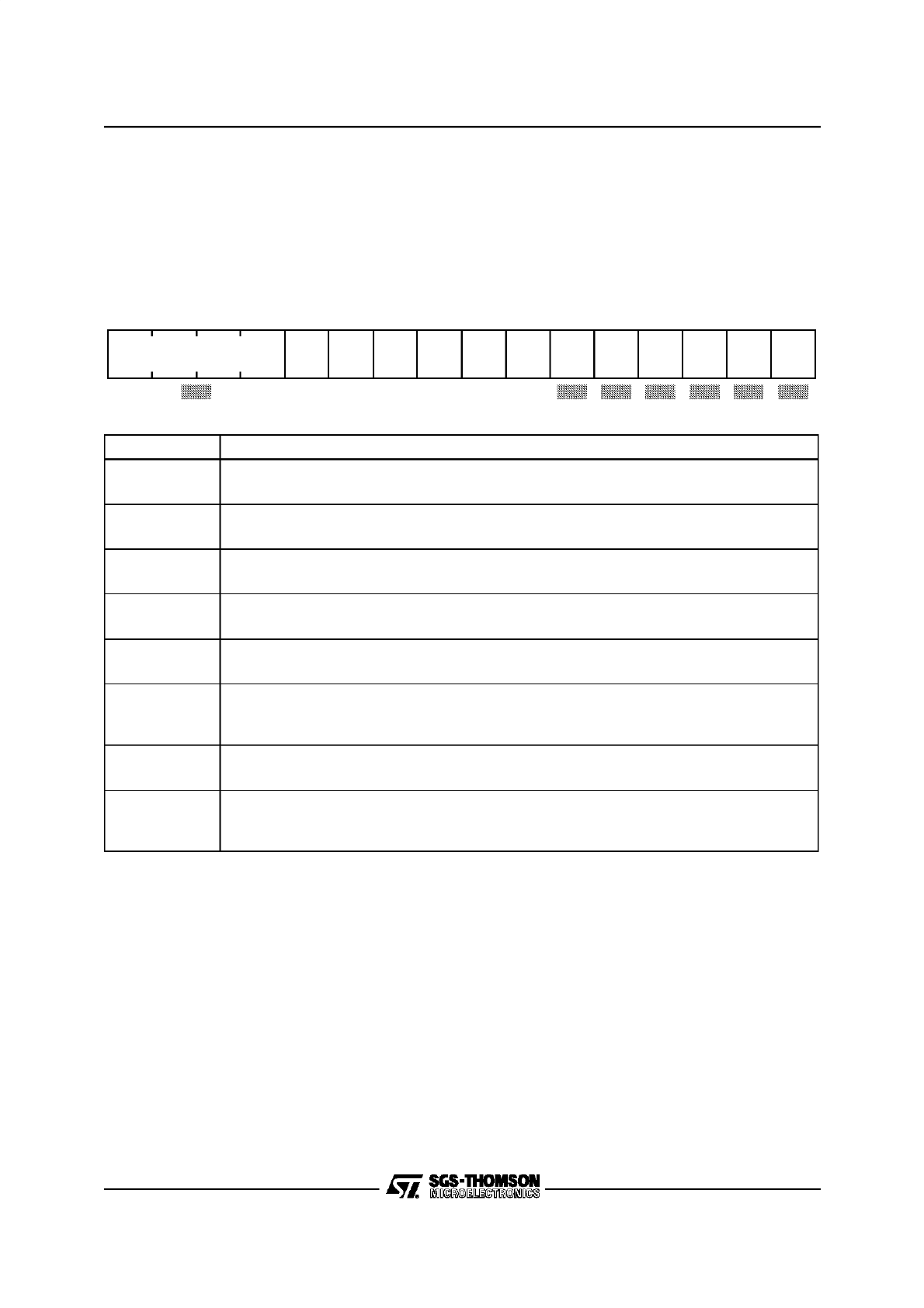
12/26
3 - CENTRAL PROCESSING UNIT (ST10R163)
CPU SPECIAL FUNCTION REGISTERS(Cont’d)
The Processor Status Word PSW
This bit-addressable register reflects the current
state of the microcontroller. Two groups of bits
represent the current ALU status, and the current
CPU interrupt status. A separate bit (USR0) within
register PSW is provided as a general purpose
user flag.
PSW (FF10h / 88h)
SFR
Reset Value: 0000h
Bit
Function
N
Negative Result
Set, when the result of an ALU operation is negative.
C
Carry Flag
Set, when the result of an ALU operation produces a carry bit.
V
Overflow Result
Set, when the result of an ALU operation produces an overflow.
Z
Zero Flag
Set, when the result of an ALU operation is zero.
E
End of Table Flag
Set, when the source operand of an instruction is 8000h or 80h.
MULIP
Multip lication/Div ision In Progress
‘0’: There is no multiplication/division in progress.
‘1’: A multiplication/division has been interrupted.
USR0
User General Purpose Flag
May be used by the application software.
HLDEN,
ILVL, IEN
Interrupt and EBC Control Fields
Define the response to interrupt requests and enable external bus arbitration. (Described in section
“Interrupt and Trap Functions”)
HLD
EN
MUL
IP
USR0
-
N
Z
C
V
E
5
4
3
2
1
0
11
10
9
8
7
6
15
14
13
12
rw
rw
rw
rw
-
rw
rw
rw
-
rw
-
rw
IEN
-
-
ILVL
rw
38

13/26
3 - CENTRAL PROCESSING UNIT (ST10R163)
CPU SPECIAL FUNCTION REGISTERS(Cont’d)
ALU Status (N, C, V, Z, E, MULIP)
The condition flags (N, C, V, Z, E) within the PSW
indicate the ALU status due to the last recently
performed ALU operation. They are set by most of
the instructions due to specific rules, which de-
pend on the ALU or data movement operation per-
formed by an instruction.
After execution of an instruction which explicitly
updates the PSW register, the condition flags can-
not be interpreted as described in the following,
because any explicit write to the PSW register su-
persedes the condition flag values, which are im-
plicitly generated by the CPU. Explicitly reading
the PSW register supplies a read value which rep-
resents the state of the PSW register after execu-
tion of the immediately preceding instruction.
Note: After reset, all of the ALU status bits are
cleared.
•
N-Flag: For most of the ALU operations, the N-
flag is set to ’1’, if the most significant bit of the re-
sult contains a ’1’, otherwise it is cleared. In the
case of integer operations the N-flag can be inter-
preted as the sign bit of the result (negative: N=’1’,
positive: N=’0’). Negative numbers are always
represented as the 2’s complement of the corre-
sponding positive number. The range of signed
numbers extends from ’–8000h’ to ’+7FFFh’ for the
word data type, or from ’–80h’ to ’+7Fh’ for the byte
data type.For Boolean bit operations with only one
operand the N-flag represents the previous state
of the specified bit. For Boolean bit operations with
two operands the N-flag represents the logical
XORing of the two specified bits.
•
C-Flag:After an addition the C-flag indicates that
a carry from the most significant bit of the speci-
fied word or byte data type has been generated.
After a subtraction or a comparison the C-flag indi-
cates a borrow, which represents the logical nega-
tion of a carry for the addition.
This means that the C-flag is set to ’1’, ifno carry
from the most significant bit of the specified word
or byte data type has been generated during a
subtraction, which is performed internally by the
ALU as a 2’s complement addition, and the C-flag
is cleared when this complement addition caused
a carry.
The C-flag is always cleared for logical, multiply
and divide ALU operations, because these opera-
tions cannot cause a carry anyhow.
For shift and rotate operations the C-flag repre-
sents the value of the bit shifted out last. If a shift
count of zero is specified, the C-flag will be
cleared. The C-flag is also cleared for a prioritize
ALU operation, because a ’1’ is never shifted out
of the MSB during the normalization of an oper-
and.
For Boolean bit operations with only one operand
the C-flag is always cleared. For Boolean bit oper-
ations with two operands the C-flag represents the
logical ANDing of the two specified bits.
•
V-Flag:For addition, subtraction and 2’s comple-
mentation the V-flag is always set to ’1’, if the re-
sult overflows the maximum range of signed num-
bers, which are representable by either 16 bits for
word operations (’–8000h’ to ’+7FFFh’), or by 8
bits for byte operations (’–80h’ to ’+7Fh’), other-
wise the V-flag is cleared. Note that the result of
an integer addition, integer subtraction, or 2’s
complement is not valid, if the V-flag indicates an
arithmetic overflow.
For multiplication and division the V-flag is set to
’1’, if the result cannot be represented in a word
data type, otherwise it is cleared. Note that a divi-
sion by zero will always cause an overflow. In con-
trast to the result of a division, the result of a mul-
tiplication is valid regardless of whether the V-flag
is set to ’1’ or not.
Since logical ALU operations cannot produce an
invalid result, the V-flag is cleared by these opera-
tions.
The V-flag is also used as ’Sticky Bit’ for rotate
right and shift right operations. With only using the
C-flag, a rounding error caused by a shift right op-
eration can be estimated up to a quantity of one
half of the LSB of the result. In conjunction with the
V-flag, the C-flag allows evaluating the rounding
error with a finer resolution (see table below).
For Boolean bit operations with only one operand
the V-flag is always cleared. For Boolean bit oper-
ations with two operands the V-flag represents the
logical ORing of the two specified bits.
Shift Right Rounding Error Evaluation
C-
Flag
V-
Flag
Rounding Error Quantit y
0
0
1
1
0
1
0
1
-
No rounding error
-
0< Rounding error
<
1
/
2
LSB
Rounding error
=
1
/
2
LSB
Rounding error
>
1
/
2
LSB
39

14/26
3 - CENTRAL PROCESSING UNIT (ST10R163)
CPU SPECIAL FUNCTION REGISTERS(Cont’d)
•
Z-Flag: The Z-flag is normally set to ’1’, if the re-
sult of an ALU operation equals zero, otherwise it
is cleared.
For the addition and substraction with carry the Z-
flag is only set to ’1’, if the Z-flag already contains
a ’1’ and the result of the current ALU operation
additionally equals zero. This mechanism is pro-
vided for the support of multiple precision calcula-
tions.
For Boolean bit operations with only one operand
the Z-flag represents the logical negation of the
previous state of the specified bit. For Boolean bit
operations with two operands the Z-flag repre-
sents the logical NORing of the two specified bits.
For the prioritize ALU operation the Z-flag indi-
cates, if the second operand was zero or not.
•
E-Flag: The E-flag can be altered by instruc-
tions, which perform ALU or data movement oper-
ations. The E-flag is cleared by those instructions
which cannot be reasonably used for table search
operations. In all other cases the E-flag is set de-
pending on the value of the source operand to sig-
nify whether the end of a search table is reached
or not. If the value of the source operand of an in-
struction equals the lowest negative number,
which is representable by the data format of the
corresponding instruction (’8000h’ for the word
data type, or ’80h’ for the byte data type), the E-
flag is set to ’1’, otherwise it is cleared.
•
MULIP-Flag:The MULIP-flag will be set to ’1’ by
hardware upon the entrance into an interrupt serv-
ice routine, when a multiply or divide ALU opera-
tion was interrupted before completion. Depend-
ing on the state of the MULIP bit, the hardware de-
cides whether a multiplication or division must be
continued or not after the end of an interrupt serv-
ice. The MULIP bit is overwritten with the contents
of the stacked MULIP-flag when the return-from-
interrupt-instruction (RETI) is executed. This nor-
mally means that the MULIP-flag is cleared again
after that.
Note: The MULIP flag is a part of the task environ-
ment! When the interrupting service routine does
not return to the interrupted multiply/divide instruc-
tion (ie. in case of a task scheduler that switches
between independent tasks), the MULIP flag must
be saved as part of the task environment and must
be updated accordingly for the new task before
this task is entered.
CPU Interrupt Status (IEN, ILVL)
The Interrupt Enable bit allows to globally enable
(IEN=’1’) or disable (IEN=’0’) interrupts. The four-
bit Interrupt Level field (ILVL) specifies the priority
of the current CPU activity. The interrupt level is
updated by hardware upon entry into an interrupt
service routine, but it can also be modified via soft-
ware to prevent other interrupts from being ac-
knowledged. In case an interrupt level ’15’ has
been assigned to the CPU, it has the highest pos-
sible priority, and thus the current CPU operation
cannot be interrupted except by hardware traps or
external non-maskable
interrupts. For details
please refer to chapter “Interrupt and Trap Func-
tions”.
After reset all interrupts are globally disabled, and
the lowest priority (ILVL=0) is assigned to the ini-
tial CPU activity.
40
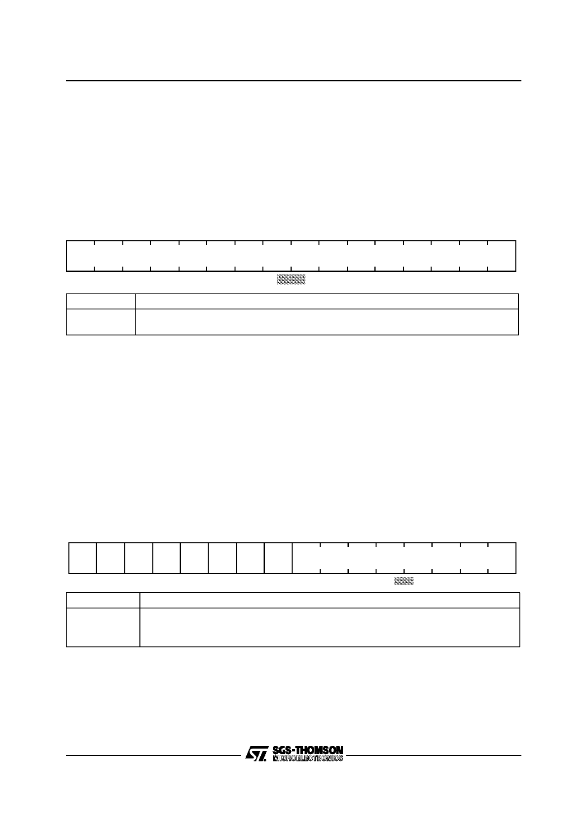
15/26
3 - CENTRAL PROCESSING UNIT (ST10R163)
CPU SPECIAL FUNCTION REGISTERS(Cont’d)
The Instruction Pointer IP
This register determines the 16-bit intra-segment
address of the currently fetched instruction within
the code segment selected by the CSP register.
The IP register is not mapped into the ST10R163’s
address space, and thus it cannot directly be ac-
cessed by the programmer. The IP can, however,
be modified indirectly via the stack by means of a
return instruction.
The IP register is implicitly updated by the CPU for
branch instructions and after instruction fetch op-
erations.
IP (---- / --)
---
Reset Value: 0000h
The Code Segment Pointer CSP
This non-bit addressable register selects the code
segment being used at run-time to access instruc-
tions. The lower 8 bits of register CSP select one
of up to 256 segments of 64 Kbytes each, while
the upper 8 bits are reserved for future use.
Code memory addresses are generated by direct-
ly extending the 16-bit contents of the IP register
by the contents of the CSP register as shown in
the figure below.
In case of the segmented memory mode the se-
lected number of segment address bits (7...0, 3...0
or 1...0) of register CSP is output on the segment
address pins A23/A19/A17...A16 of Port 4 for all
external code accesses. For non-segmented
memory mode or Single Chip Mode the content of
this register is not significant, because all code ac-
cesses are automatically restricted to segment 0.
Note: The CSP register can only be read but not
written by data operations. It is, however, modified
either directly by means of the JMPS and CALLS
instructions, or indirectly via the stack by means of
the RETS and RETI instructions.
Upon the acceptance of an interrupt or the execu-
tion of a software TRAP instruction, the CSP reg-
ister is automatically set to zero.
CSP (FE08h / 04h)
SFR
Reset Value: 0000h
Bit
Fun ction
ip
Specifies the intra segment offset, from where the current instruction is to be fetched. IP refers to
the current segment <SEGNR>.
5
4
3
2
1
0
11
10
9
8
7
6
15
14
13
12
(r)(w)
ip
Bit
Fun ction
SEGNR
Segment Number
Specifies the code segment, from where the current instruction is to be fetched. SEGNR is ignored
when segmentation is disabled.
-
-
-
-
-
5
4
3
2
1
0
11
10
9
8
7
6
15
14
13
12
-
-
-
r
-
-
-
-
-
-
-
-
SEGNR
41
16/26
3 - CENTRAL PROCESSING UNIT (ST10R163)
CPU SPECIAL FUNCTION REGISTERS(Cont’d)
Figure 3-5. Addressing via the Code Segment Pointer
Note: When segmentation is disabled, the IP value is used directly as the 16-bit address.
0
1
255
254
Code Segment
00’0000h
FF’FFFFh
01’0000h
FE’0000h
CSP Register
IP Register
0
0
15
15
24/20/18 bit Physical Code Address
42
17/26
3 - CENTRAL PROCESSING UNIT (ST10R163)
CPU SPECIAL FUNCTION REGISTERS(Cont’d)
The Data Page Pointers DPP0, DPP1, DPP2,
DPP3
These four non-bit addressable registers select up
to four different data pages being active simulta-
neously at run-time. The lower 10 bits of each
DPP register select one of the 1024 possible 16-
Kbyte data pages while the upper 6 bits are re-
served for future use. The DPP registers allow to
access the entire memory space in pages of 16
Kbytes each.
The DPP registers are implicitly used, whenever
data accesses to any memory location are made
via indirect or direct long 16-bit addressing modes
(except for override accesses via EXTended in-
structions and PEC data transfers). After reset,
the Data Page Pointers are initialized in a way that
all indirect or direct long 16-bit addresses result in
identical 18-bit addresses. This allows to access
data pages 3...0 within segment 0 as shown in the
figure below. If the user does not want to use any
data paging, no further action is required.
DPP0 (FE00h / 00h)
SFR
Reset Value: 0000h
DPP1 (FE02h / 01h)
SFR
Reset Value: 0001h
DPP2 (FE04h / 02h)
SFR
Reset Value: 0002h
DPP3 (FE06h / 03h)
SFR
Reset Value: 0003h
Bit
Fun ction
DPPxPN
Data Page Number of DPPx
Specifies the data page selected via DPPx. Only the least significant two bits of DPPx are sig-
nificant when segmentation is disabled.
-
-
-
5
4
3
2
1
0
11
10
9
8
7
6
15
14
13
12
-
rw
-
-
-
-
-
-
-
-
DPP0PN
-
-
-
5
4
3
2
1
0
11
10
9
8
7
6
15
14
13
12
-
rw
-
-
-
-
-
-
-
-
DPP1PN
-
-
-
5
4
3
2
1
0
11
10
9
8
7
6
15
14
13
12
-
rw
-
-
-
-
-
-
-
-
DPP2PN
-
-
-
5
4
3
2
1
0
11
10
9
8
7
6
15
14
13
12
-
rw
-
-
-
-
-
-
-
-
DPP3PN
43
18/26
3 - CENTRAL PROCESSING UNIT (ST10R163)
CPU SPECIAL FUNCTION REGISTERS(Cont’d)
Data paging is performed by concatenating the
lower 14 bits of an indirect or direct long 16-bit ad-
dress with the contents of the DDP register select-
ed by the upper two bits of the 16-bit address. The
content of the selected DPP register specifies one
of the 1024 possible data pages. This data page
base address together with the 14-bit page offset
forms the physical 24/20/18-bit address.
In case of non-segmented memory mode, only the
two least significant bits of the implicitly selected
DPP register are used to generate the physical
address. Thus, extreme care should be taken
when changing the content of a DPP register, if a
non-segmented memory model is selected, be-
cause otherwise unexpected results could occur.
In case of the segmented memory mode the se-
lected number of segment address bits (9...2, 5...2
or 3...2) of the respective DPP register is output on
the segment address pins A23/A19/A17...A16 of
Port 4 for all external data accesses.
A DPP register can be updated via any instruction,
which is capable of modifying an SFR.
Note: Due to the internal instruction pipeline, a
new DPP value is not yet usable for the operand
address calculation of the instruction immediately
following the instruction updating the DPP regis-
ter.
Figure 3-6. Addressing via the Data Page Pointers
1023
Data Pages
16-bit Data Address
0
15 14
14-bit
Intra-Page Address
(concatenated with
content of DPPx)
1022
1021
2
1
0
3
DPP3
DPP2
DPP1
DPP0
1 1
1 0
0 1
0 0
DPP Registers
After reset or with segmentation disabled the DPP registers select data pages 3...0.
All of the internal memory is accessible in these cases.
44
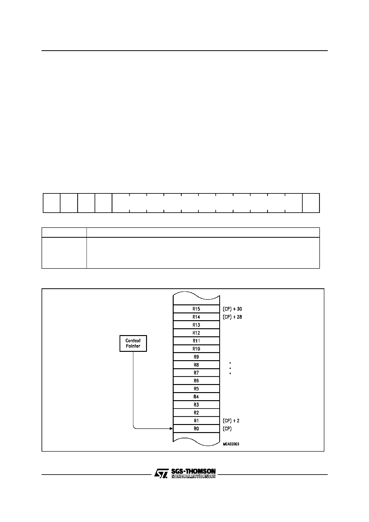
19/26
3 - CENTRAL PROCESSING UNIT (ST10R163)
CPU SPECIAL FUNCTION REGISTERS(Cont’d)
The Context Pointer CP
This non-bit addressable register is used to select
the current register context. This means that the
CP register value determines the address of the
first General Purpose Register (GPR) within the
current register bank of up to 16 wordwide and/or
bytewide GPRs.
Note: It is the user’s responsibility that the physi-
cal GPR address specified via CP register plus
short GPR address must always be an internal
RAM location. If this condition is not met, unex-
pected results may occur.
– Do not set CP below 00’F600h or above 00’FDFEh
– Be careful using the upper GPRs with CP above
00’FDE0h
The CP register can be updated via any instruc-
tion which is capable of modifying an SFR.
Note: Due to the internal instruction pipeline, a
new CP value is not yet usable for GPR address
calculations of the instruction immediately follow-
ing the instruction updating the CP register.
The Switch Context instruction (SCXT) allows to
save the content of register CP on the stack and
updating it with a new value in just one machine
cycle.
CP (FE10h / 08h)
SFR
Reset Value: FC00h
Figure 3-7Register Bank Selection via Register CP
Bit
Functio n
cp
Modifiable portion of register CP
Specifies the (word) base address of the current register bank.
When writing a value to register CP with bits CP.11...CP.9 = ‘000’, bits CP.11...CP.10 are set to
‘11’ by hardware, in all other cases all bits of bit field “cp” receive the written value.
1
0
1
5
4
3
2
1
0
11
10
9
8
7
6
15
14
13
12
r
rw
r
r
r
1
1
r
cp
45
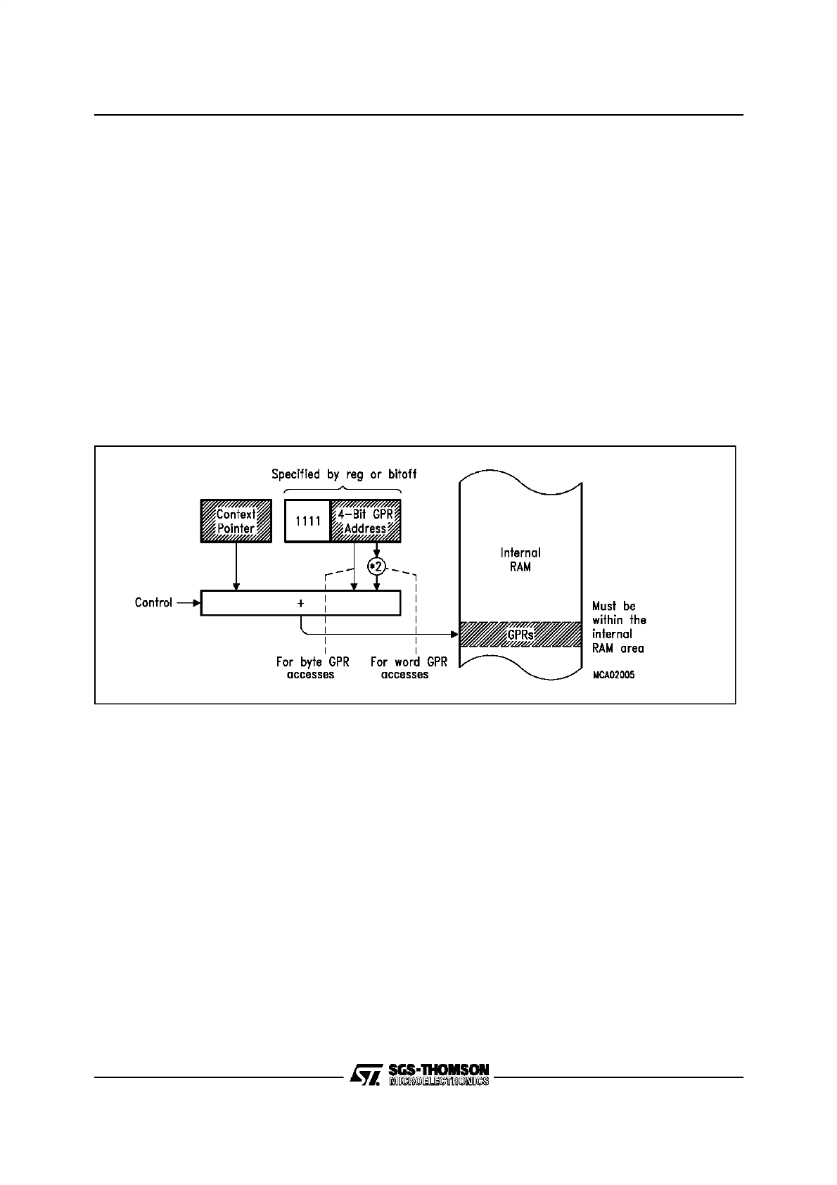
20/26
3 - CENTRAL PROCESSING UNIT (ST10R163)
CPU SPECIAL FUNCTION REGISTERS(Cont’d)
Several addressing modes use register CP implic-
itly for address calculations. The addressing
modes mentioned below are described in chapter
“Instruction Set Summary”.
Short 4-Bit GPR Addresses (mnemonic: Rw or
Rb) specify an address relative to the memory lo-
cation specified by the contents of the CP register,
ie. the base of the current register bank.
Depending on whether a relative word (Rw) or
byte (Rb) GPR address is specified, the short 4-bit
GPR address is either multiplied by two or not be-
fore it is added to the content of register CP (see
figure below). Thus, both byte and word GPR ac-
cesses are possible in this way.
GPRs used as indirect address pointers are al-
ways accessed wordwise. For some instructions
only the first four GPRs can be used as indirect
address pointers. These GPRs are specified via
short 2-bit GPR addresses. The respective physi-
cal address calculation is identical to that for the
short 4-bit GPR addresses.
Short 8-Bit Register Addresses (mnemonic: reg
or bitoff) within a range from F0h to FFh interpret
the four least significant bits as short 4-bit GPR
address, while the four most significant bits are ig-
nored. The respective physical GPR address cal-
culation is identical to that for the short 4-bit GPR
addresses. For single bit accesses on a GPR, the
GPR’s word address is calculated as just de-
scribed, but the position of the bit within the word
is specified by a separate additional 4-bit value.
Figure 3-8. Implicit CP Use by Short GPR Addressing Modes
46
21/26
3 - CENTRAL PROCESSING UNIT (ST10R163)
CPU SPECIAL FUNCTION REGISTERS(Cont’d)
The Stack Pointer SP
This non-bit addressable register is used to point
to the top of the internal system stack (TOS). The
SP register is pre-decremented whenever data is
to be pushed onto the stack, and it is post-incre-
mented whenever data is to be popped from the
stack. Thus, the system stack grows from higher
toward lower memory locations.
Since the least significant bit of register SP is tied
to ’0’ and bits 15 through 12 are tied to ’1’ by hard-
ware, the SP register can only contain values from
F000h to FFFEh. This allows to access a physical
stack within the internal RAM of the ST10R163. A
virtual stack (usually bigger) can be realized via
software. This mechanism is supported by regis-
ters STKOV and STKUN (see respective descrip-
tions below).
The SP register can be updated via any instruc-
tion, which is capable of modifying an SFR.
Note: Due to the internal instruction pipeline, a
POP or RETURN instruction must not immediately
follow an instruction updating the SP register.
SP (FE12h / 09h)
SFR
Reset Value: FC00h
Bit
Function
sp
Modifiable portion of register SP
Specifies the top of the internal system stack.
1
0
1
5
4
3
2
1
0
11
10
9
8
7
6
15
14
13
12
r
rw
r
r
r
1
1
r
sp
47
22/26
3 - CENTRAL PROCESSING UNIT (ST10R163)
CPU SPECIAL FUNCTION REGISTERS(Cont’d)
The Stack Overflow Pointer STKOV
This non-bit addressable register is compared
against the SP register after each operation,
which pushes data onto the system stack (eg.
PUSH and CALL instructions or interrupts) and af-
ter each substraction from the SP register. If the
content of the SP register is less than the content
of the STKOV register, a stack overflow hardware
trap will occur.
Since the least significant bit of register STKOV is
tied to ’0’ and bits 15 through 12 are tied to ’1’ by
hardware, the STKOV register can only contain
values from F000h to FFFEh.
The Stack Overflow Trap (entered when (SP) <
(STKOV)) may be used in two different ways:
•
Fatal error indicationtreats the stack overflow
as a system error through the associated trap
service routine. Under these circumstances data
in the bottom of the stack may have been overwrit-
ten by the status information stacked upon servic-
ing the stack overflow trap.
•
Automatic system stack flushingallows to use
the system stack as a ’Stack Cache’ for a bigger
external user stack. In this case register STKOV
should be initialized to a value, which represents
the desired lowest Top of Stack address plus 12
according to the selected maximum stack size.
This considers the worst case that will occur,
when a stack overflow condition is detected just
during entry into an interrupt service routine.
Then, six additional stack word locations are re-
quired to push IP, PSW, and CSP for both the in-
terrupt service routine and the hardware trap serv-
ice routine.
More details about the stack overflow trap service
routine and virtual stack management are given in
chapter “System Programming”.
STKOV (FE14h / 0Ah)
SFR
Reset Value: FA00h
Bit
Function
stkov
Modif iable portio n of register STKOV
Specifies the lower limit of the internal system stack.
1
0
1
5
4
3
2
1
0
11
10
9
8
7
6
15
14
13
12
r
rw
r
r
r
1
1
r
stkov
48
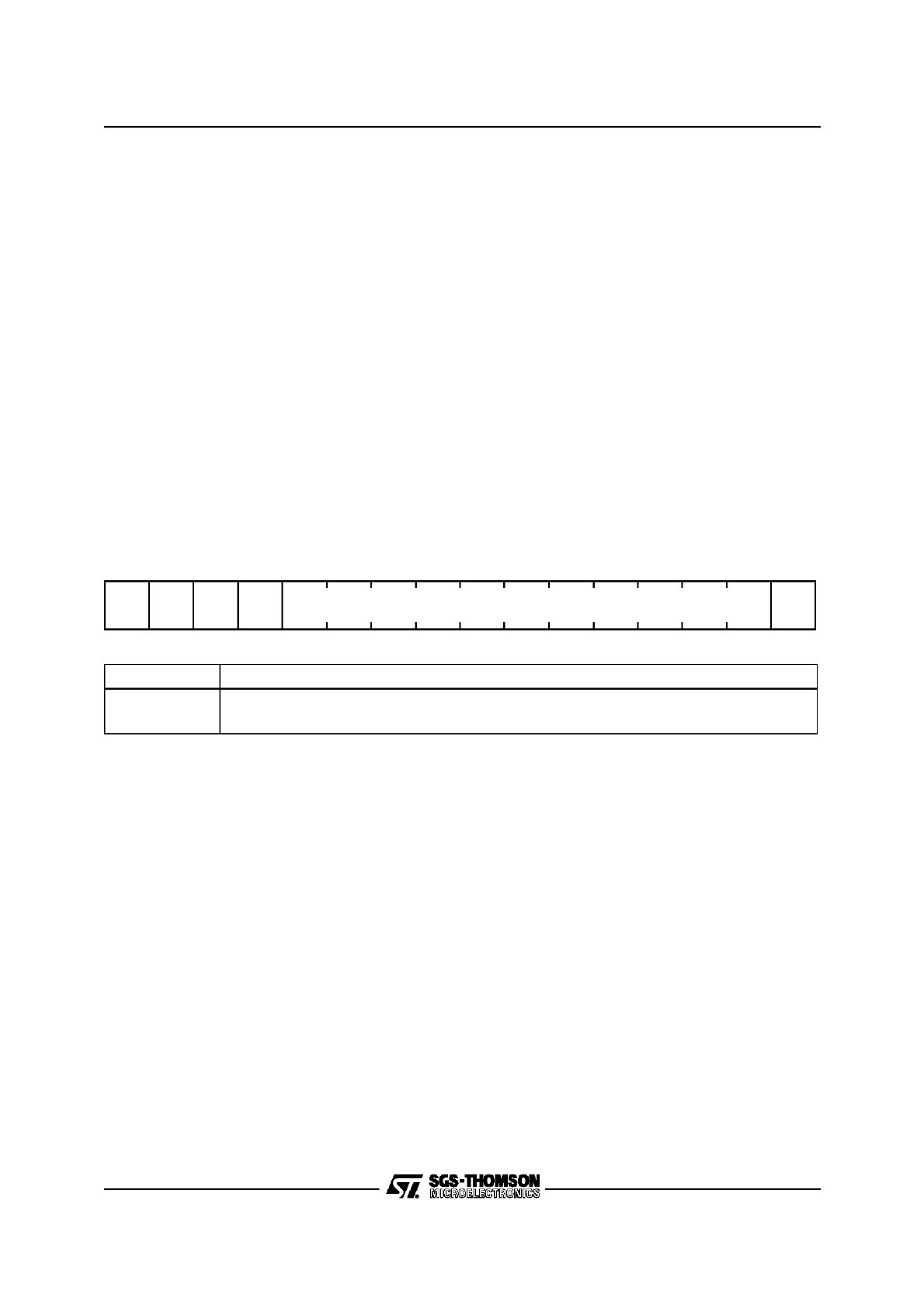
23/26
3 - CENTRAL PROCESSING UNIT (ST10R163)
CPU SPECIAL FUNCTION REGISTERS(Cont’d)
The Stack Underflow Pointer STKUN
This non-bit addressable register is compared
against the SP register after each datapop opera-
tion from the system stack (eg. POP and RET in-
structions) and after each addition to the SP regis-
ter. If the content of the SP register is greater than
the content of the STKUN register, a stack under-
flow hardware trap will occur.
Since the least significant bit of register STKUN is
tied to ’0’ and bits 15 through 12 are tied to ’1’ by
hardware, the STKUN register can only contain
values from F000h to FFFEh.
The Stack Underflow Trap (entered when (SP) >
(STKUN)) may be used in two different ways:
•
Fatal error indicationtreats the stack underflow
as a system error through the associated trap
service routine.
•
Automatic system stack refillingallows to use
the system stack as a ’Stack Cache’ for a bigger
external user stack. In this case register STKUN
should be initialized to a value, which represents
the desired highest Bottom of Stack address.
More details about the stack underflow trap serv-
ice routine and virtual stack management are giv-
en in chapter “System Programming”.
Scope of Stack Limit Control
The stack limit control realized by the register pair
STKOV and STKUN detects cases where the
stack pointer SP is moved outside the defined
stack area either by ADD or SUB instructions or by
PUSH or POP operations (explicit or implicit, ie.
CALL or RET instructions).
This control mechanism is not triggered, ie. no
stack trap is generated, when
– the stack pointer SP is directly updated via MOV
instructions
– the limits of the stack area (STKOV, STKUN) are
changed, so that SP is outside of the new limits.
STKUN (FE16h / 0Bh)
SFR
Reset Value: FC00h
Bit
Function
stkun
Modifiable portion of register STKUN
Specifies the upper limit of the internal system stack.
1
0
1
5
4
3
2
1
0
11
10
9
8
7
6
15
14
13
12
r
rw
r
r
r
1
1
r
stkun
49
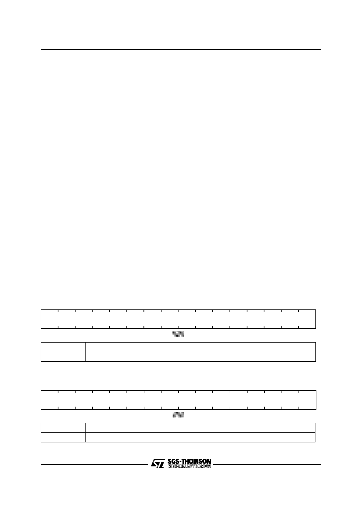
24/26
3 - CENTRAL PROCESSING UNIT (ST10R163)
CPU SPECIAL FUNCTION REGISTERS(Cont’d)
The Multiply/Divide High Register MDH
This register is a part of the 32-bit multiply/divide
register, which is implicitly used by the CPU, when
it performs a multiplication or a division. After a
multiplication, this non-bit addressable register
represents the high order 16 bits of the 32-bit re-
sult. For long divisions, the MDH register must be
loaded with the high order 16 bits of the 32-bit div-
idend before the division is started. After any divi-
sion, register MDH represents the 16-bit remain-
der.
Whenever this register is updated via software,
the Multiply/Divide Register In Use (MDRIU) flag
in the Multiply/Divide Control register (MDC) is set
to ’1’.
When a multiplication or division is interrupted be-
fore its completion and when a new multiply or di-
vide operation is to be performed within the inter-
rupt service routine, register MDH must be saved
along with registers MDL and MDC to avoid erro-
neous results.
A detailed description of how to use the MDH reg-
ister for programming multiply and divide algo-
rithms can be found in chapter “System Program-
ming”.
The Multiply/Divide Low Register MDL
This register is a part of the 32-bit multiply/divide
register, which is implicitly used by the CPU, when
it performs a multiplication or a division. After a
multiplication, this non-bit addressable register
represents the low order 16 bits of the 32-bit re-
sult. For long divisions, the MDL register must be
loaded with the low order 16 bits of the 32-bit divi-
dend before the division is started. After any divi-
sion, register MDL represents the 16-bit quotient.
Whenever this register is updated via software,
the Multiply/Divide Register In Use (MDRIU) flag
in the Multiply/Divide Control register (MDC) is set
to ’1’. The MDRIU flag is cleared, whenever the
MDL register is read via software.
When a multiplication or division is interrupted be-
fore its completion and when a new multiply or di-
vide operation is to be performed within the inter-
rupt service routine, register MDL must be saved
along with registers MDH and MDC to avoid erro-
neous results.
A detailed description of how to use the MDL reg-
ister for programming multiply and divide algo-
rithms can be found in chapter “System Program-
ming”.
MDH (FE0Ch / 06h)
SFR
Reset Value: 0000h
MDL (FE0Eh / 07h)
SFR
Reset Value: 0000h
Bit
Function
mdh
Specifies the high order 16 bits of the 32-bit multiply and divide register MD.
Bit
Function
mdl
Specifies the low order 16 bits of the 32-bit multiply and divide register MD.
5
4
3
2
1
0
11
10
9
8
7
6
15
14
13
12
rw
mdh
5
4
3
2
1
0
11
10
9
8
7
6
15
14
13
12
rw
mdl
50
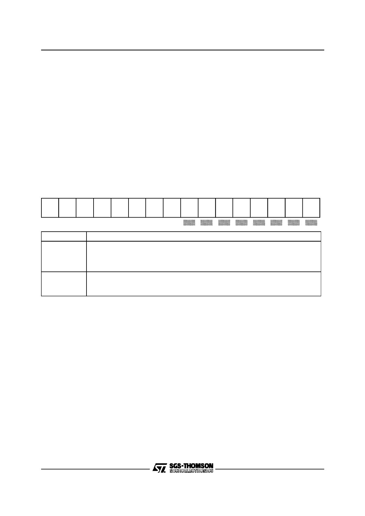
25/26
3 - CENTRAL PROCESSING UNIT (ST10R163)
CPU SPECIAL FUNCTION REGISTERS(Cont’d)
The Multiply/Divide Control Register MDC
This bit addressable 16-bit register is implicitly
used by the CPU, when it performs a multiplication
or a division. It is used to store the required control
information for the corresponding multiply or di-
vide operation. Register MDC is updated by hard-
ware during each single cycle of a multiply or di-
vide instruction.
When a division or multiplication was interrupted
before its completion and the multiply/divide unit is
required, the MDC register must first be saved
along with registers MDH and MDL (to be able to
restart the interrupted operation later), and then it
must be cleared to be prepared for the new calcu-
lation. After completion of the new division or mul-
tiplication, the state of the interrupted multiply or
divide operation must be restored.
The MDRIU flag is the only portion of the MDC
register which might be of interest for the user.
The remaining portions of the MDC register are re-
served for dedicated use by the hardware, and
should never be modified by the user in another
way as described above. Otherwise, a correct
continuation of an interrupted multiply or divide
operation cannot be guaranteed.
A detailed description of how to use the MDC reg-
ister for programming multiply and divide algo-
rithms can be found in chapter “System Program-
ming”.
MDC (FF0Eh / 87h)
SFR
Reset Value: 0000h
Bit
Function
MDRIU
Multiply/Divide Register In Use
‘0’:Cleared, when register MDL is read via software.
‘1’:Set when register MDL or MDH is written via software, or when a multiply
or divide instruction is executed.
!!
Internal Machine Status
The multiply/divide unit uses these bits to control internal operations.
Never modify these bits without saving and restoring register MDC.
-
!!
-
-
5
4
3
2
1
0
11
10
9
8
7
6
15
14
13
12
-
r(w)
-
-
-
-
-
-
-
-
!!
!!
!!
!!
!!
!!
-
-
-
-
r(w)
r(w)
r(w)
r(w)
r(w)
r(w)
r(w)
MDR
IU
51

26/26
3 - CENTRAL PROCESSING UNIT (ST10R163)
CPU SPECIAL FUNCTION REGISTERS(Cont’d)
The Constant Zeros Register ZEROS
All bits of this bit-addressable register are fixed to
’0’ by hardware. This register can be read only.
Register ZEROS can be used as a register-ad-
dressable constant of all zeros, ie. for bit manipu-
lation or mask generation. It can be accessed via
any instruction, which is capable of addressing a
SFR.
The Constant Ones Register ONES
All bits of this bit-addressable register are fixed to
’1’ by hardware. This register can be read only.
Register ONES can be used as a register-ad-
dressable constant of all ones, ie. for bit manipula-
tion or mask generation. It can be accessed via
any instruction, which is capable of addressing an
SFR.
ZEROS (FF1Ch / 8Eh)
SFR
Reset Value: 0000h
ONES (FF1Eh / 8Fh)
SFR
Reset Value: FFFFh
0
0
0
0
0
5
4
3
2
1
0
11
10
9
8
7
6
15
14
13
12
r
r
r
r
r
r
0
0
0
r
0
0
0
0
0
0
0
0
r
r
r
r
r
r
r
r
r
1
1
1
1
1
5
4
3
2
1
0
11
10
9
8
7
6
15
14
13
12
r
r
r
r
r
r
1
1
1
r
1
1
1
1
1
1
1
1
r
r
r
r
r
r
r
r
r
52

February 1996
1/24
This is advance information from SGS-TH OMSON. Details are subject tochange without notice.
ST10R163
User Manual
4 - INTERRUPT AND TRAP FUNCTIONS
The architecture of the ST10R163 supports sever-
al mechanisms for fast and flexible response to
service requests that can be generated from vari-
ous sources internal or external to the microcon-
troller.
These mechanisms include:
Normal Interrupt Processing
The CPU temporarily suspends the current pro-
gram execution and branches to an interrupt serv-
ice routine in order to service an interrupt request-
ing device. The current program status (IP, PSW,
in segmentation mode also CSP) is saved on the
internal system stack. A prioritization scheme with
16 priority levels allows the user to specify the or-
der in which multiple interrupt requests are to be
handled.
Interrupt Processing via the Peripheral Event
Controller (PEC)
A faster alternative to normal software controlled
interrupt processing is servicing an interrupt re-
questing device with the ST10R163’s integrated
Peripheral Event Controller (PEC). Triggered by
an interrupt request, the PEC performs a single
word or byte data transfer between any two loca-
tions in segment 0 (data pages 0 through 3)
through one of eight programmable PEC Service
Channels. During a PEC transfer the normal pro-
gram execution of the CPU is halted for just 1 in-
struction cycle. No internal program status infor-
mation needs to be saved. The same prioritization
scheme is used for PEC service as for normal in-
terrupt processing. PEC transfers share the 2
highest priority levels.
Trap Functions
Trap functions are activated in response to special
conditions that occur during the execution of in-
structions. A trap can also be caused externally by
the Non-Maskable Interrupt pin NMI. Several
hardware trap functions are provided for handling
erroneous conditions and exceptions that arise
during the execution of an instruction. Hardware
traps always have highest priority and cause im-
mediate system reaction. The software trap func-
tion is invoked by the TRAP instruction, which
generates a software interrupt for a specified inter-
rupt vector. For all types of traps the current pro-
gram status is saved on the system stack.
External Interrupt Processing
Although the ST10R163 does not provide dedicat-
ed interrupt pins, it allows to connect external in-
terrupt sources and provides several mechanisms
to react on external events, including standard in-
puts, non-maskable interrupts and fast external in-
terrupts. These interrupt functions are alternate
port functions, except for the non-maskable inter-
rupt and the reset input.
53

2/24
4 - INTERRUPT AND TRAP FUNCTIONS (ST10R163)
4.1 INTERRUPT SYSTEM STRUCTURE
The ST10R163 provides 20 separate interrupt
nodes that may be assigned to 16 priority levels.
In order to support modular and consistent soft-
ware design techniques, each source of an inter-
rupt or PEC request is supplied with a separate in-
terrupt control register and interrupt vector. The
control register contains the interrupt request flag,
the interrupt enable bit, and the interrupt priority of
the associated source. Each source request is ac-
tivated by one specific event, depending on the
selected operating mode of the respective device.
The only exceptions are the two serial channels of
the ST10R163, where an error interrupt request
can be generated by different kinds of error. How-
ever, specific status flags which identify the type of
error are implemented in the serial channels’ con-
trol registers.
The ST10R163 provides a vectored interrupt sys-
tem. In this system specific vector locations in the
memory space are reserved for the reset, trap,
and interrupt service functions. Whenever a re-
quest occurs, the CPU branches to the location
that is associated with the respective interrupt
source. This allows direct identification of the
source that caused the request. The only excep-
tions are the class B hardware traps, which all
share the same interrupt vector. The status flags
in the Trap Flag Register (TFR) can then be used
to determine which exception caused the trap. For
the special software TRAP instruction, the vector
address is specified by the operand field of the in-
struction, which is a seven bit trap number.
The reserved vector locations build a jump table in
the low end of the ST10R163’s address space
(segment 0). The jump table is made up of the ap-
propriate jump instructions that transfer control to
the interrupt or trap service routines, which may
be located anywhere within the address space.
The entries to the jump table are located at the
lowest addresses in code segment 0 of the ad-
dress space. Each entry occupies 2 words, except
for the reset vector and the hardware trap vectors,
which occupy 4 or 8 words.
The table below lists all sources that are capable
of requesting interrupt or PEC service in the
ST10R163, the associated interrupt vectors, their
locations and the associated trap numbers. It also
lists the mnemonics of the affected Interrupt Re-
quest flags and their corresponding Interrupt Ena-
ble flags. The mnemonics are composed of a part
that specifies the respective source, followed by a
part that specifies their function (IR=Interrupt Re-
quest flag, IE=Interrupt Enable flag).
Note: The two X-Peripheral nodes in the table are pre-
pared to accept interrupt requests, one of them is
connected to the PLL Unlock interrupt request and
another one is connected to the SSP X-Peripheral
Receive/Transmit interrupt request.
The “External Interrupt Nodes” use naming conven-
tions that are compatible with the respective
ST10F167 and ST10R165 interrupt nodes
54

3/24
4 - INTERRUPT AND TRAP FUNCTIONS (ST10R163)
INTERRUPT SYSTEM STRUCTURE(Cont’d)
Note: Each entry of the interrupt vector table provides room for two word instructions or one doubleword instruction. The
respective vector location results from multiplying the trap number by 4 (4 bytes per entry).
Source of Interrupt or PEC
Service Request
Request
Flag
Enable
Flag
Interrupt
Vector
Vector
Location
Trap
Number
External Interrupt 0
CC8IR
CC8IE
CC8INT
00’0060h
18h / 24
External Interrupt 1
CC9IR
CC9IE
CC9INT
00’0064h
19h / 25
External Interrupt 2
CC10IR
CC10IE
CC10INT
00’0068h
1Ah / 26
External Interrupt 3
CC11IR
CC11IE
CC11INT
00’006Ch
1b h/ 27
External Interrupt 4
CC12IR
CC12IE
CC12INT
00’0070h
1Ch / 28
External Interrupt 5
CC13IR
CC13IE
CC13INT
00’0074h
1Dh / 29
External Interrupt 6
CC14IR
CC14IE
CC14INT
00’0078h
1Eh / 30
External Interrupt 7
CC15IR
CC15IE
CC15INT
00’007Ch
1Fh / 31
GPT1 Timer 2
T2IR
T2IE
T2INT
00’0088h
22h / 34
GPT1 Timer 3
T3IR
T3IE
T3INT
00’008Ch
23h / 35
GPT1 Timer 4
T4IR
T4IE
T4INT
00’0090h
24h / 36
GPT2 Timer 5
T5IR
T5IE
T5INT
00’0094h
25h / 37
GPT2 Timer 6
T6IR
T6IE
T6INT
00’0098h
26h / 38
GPT2 CAPREL Register
CRIR
CRIE
CRINT
00’009Ch
27h / 39
ASC0 Transmit
S0TIR
S0TIE
S0TINT
00’00A8h
2Ah / 42
ASC0 Transmit Buffer
S0TBIR
S0TBIE
S0TBINT
00’011Ch
47h / 71
ASC0 Receive
S0RIR
S0RIE
S0RINT
00’00ACh
2Bh / 43
ASC0 Error
S0EIR
S0EIE
S0EINT
00’00B0h
2Ch / 44
X-Peripheral Node 1
XP1IR
XP1IE
XP1INT
00’0104h
41h / 65
X-Peripheral Node 3
XP3IR
XP3IE
XP3INT
00’010Ch
43h / 67
55

4/24
4 - INTERRUPT AND TRAP FUNCTIONS (ST10R163)
INTERRUPT SYSTEM STRUCTURE(Cont’d)
The table below lists the vector locations for hard-
ware traps and the corresponding status flags in
register TFR. It also lists the priorities of trap serv-
ice for cases, where more than one trap condition
might be detected within the same instruction. Af-
ter any reset (hardware reset, software reset in-
struction SRST, or reset by watchdog timer over-
flow) program execution starts at the reset vector
at location 00’0000h. Reset conditions have prior-
ity over every other system activity and therefore
have the highest priority (trap priority III).
Software traps may be performed from any vector
location between 00’0000h and 00’01FCh. A serv-
ice routine entered via a software TRAP instruc-
tion is always executed on the current CPU priority
level which is indicated in bit field ILVL in register
PSW. This means that routines entered via the
software TRAP instruction can be interrupted by
all hardware traps or higher level interrupt re-
quests.
Exception Condition
Trap
Flag
Trap
Vector
Vector
Location
Trap
Number
Trap
Priority
Reset Functions:
Hardware Reset
Software Reset
Watchdog Timer Overflow
RESET
RESET
RESET
00’0000h
00’0000h
00’0000h
00h
00h
00h
III
III
III
Class A Hardware Traps:
Non-Maskable Interrupt
Stack Overflow
Stack Underflow
NMI
STKOF
STKUF
NMITRAP
STOTRAP
STUTRAP
00’0008h
00’0010h
00’0018h
02h
04h
06h
II
II
II
Class B Hardware Traps:
Undefined Opcode
Protected Instruction Fault
Illegal Word Operand Access
Illegal Instruction Access
Illegal External Bus Access
UNDOPC
PRTFLT
ILLOPA
ILLINA
ILLBUS
BTRAP
BTRAP
BTRAP
BTRAP
BTRAP
00’0028h
00’0028h
00’0028h
00’0028h
00’0028h
0Ah
0Ah
0Ah
0Ah
0Ah
I
I
I
I
I
Reserved
[2Ch – 3Ch]
[0Bh – 0Fh]
Software Traps
TRAP Instruction
Any
[00’0000h –
00’01FC h]
in steps
of 4h
Any
[00h – 7Fh]
Current
CPU Priority
56
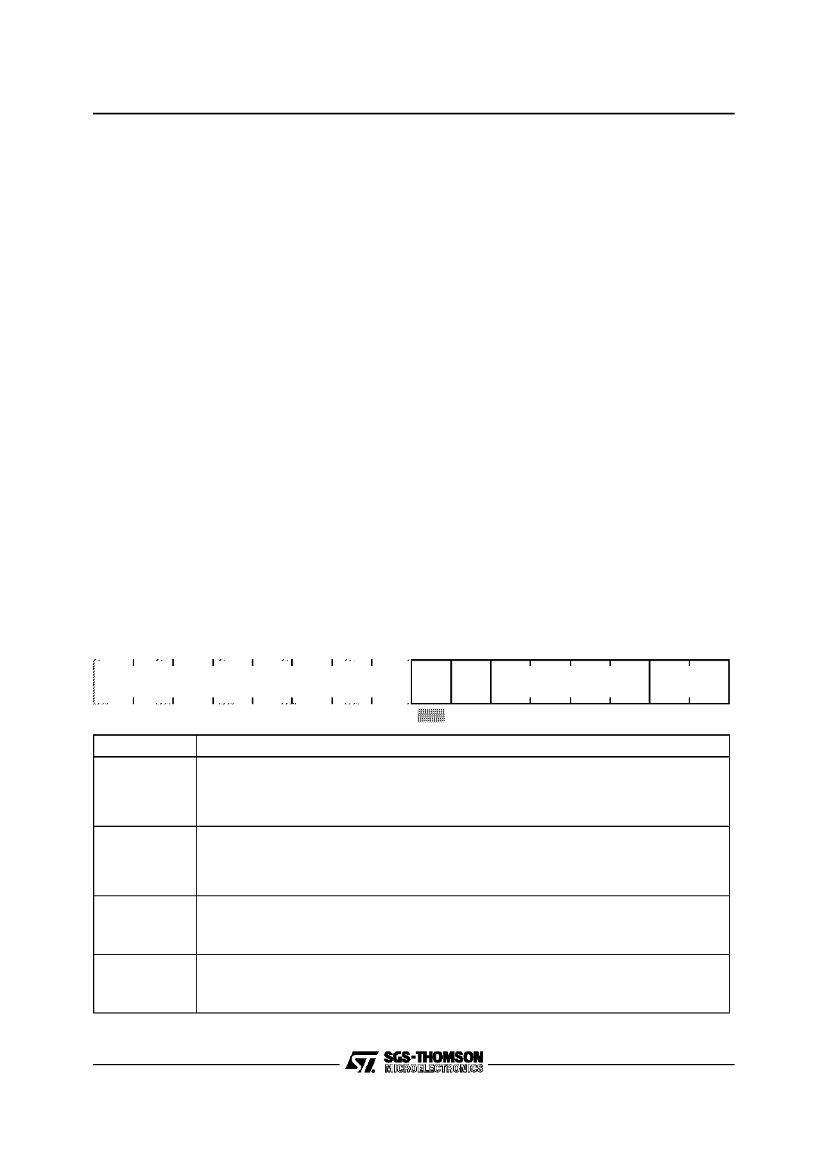
5/24
4 - INTERRUPT AND TRAP FUNCTIONS (ST10R163)
INTERRUPT SYSTEM STRUCTURE(Cont’d)
Normal Interrupt Processing and PEC Service
During each instruction cycle one out of all sourc-
es which require PEC or interrupt processing is
selected according to its interrupt priority. This pri-
ority of interrupts and PEC requests is program-
mable in two levels. Each requesting source can
be assigned to a specific priority. A second level
(“group priority”) allows to specify an internal order
for simultaneous requests from a group of differ-
ent sources on the same priority level. At the end
of each instruction cycle the source request with
the highest current priority will be determined by
the interrupt system. This request will then be
serviced, if its priority is higher than the current
CPU priority in register PSW.
Interrupt System Register Description
Interrupt processing is controlled globally by regis-
ter PSW through a general interrupt enable bit
(IEN) and the CPU priority field (ILVL). Additional-
ly the different interrupt sources are controlled in-
dividually by their specific interrupt control regis-
ters (...IC). Thus, the acceptance of requests by
the CPU is determined by both the individual inter-
rupt control registers and the PSW. PEC services
are controlled by the respective PECCx register
and the source and destination pointers, which
specify the task of the respective PEC service
channel.
Interrupt Control Registers
All interrupt control registers are organized identi-
cally. The lower 8 bits of an interrupt control regis-
ter contain the complete interrupt status informa-
tion of the associated source, which is required
during one round of prioritization, the upper 8 bits
of the respective register are reserved.. All inter-
rupt control registers are bit-addressable and all
bits can be read or written via software. This al-
lows each interrupt source to be programmed or
modified with just one instruction. When access-
ing interrupt control registers through instructions
which operate on word data types, their upper 8
bits (15...8) will return zeros, when read, and will
discard written data.
The layout of the Interrupt Control registers shown
below applies to each xxIC register, where xx
stands for the mnemonic for the respective
source.
xxIC (yyyyh / zzh)
<SFR area>
Reset Value: - - 00h
Bit
Function
GLVL
Group Level
Defines the internal order for simultaneous requests of the same priority.
3: Highest group priority
0: Lowest group priority
ILVL
Interrupt Priority Level
Defines the priority level for the arbitration of requests.
Fh: Highest priority level
0h: Lowest priority level
xxIE
Interrupt Enable Control Bit (individually enables/disables a specific source)
‘0’: Interrupt request is disabled
‘1’: Interrupt Request is enabled
xxIR
Interrupt Request Flag
‘0’: No request pending
‘1’: This source has raised an interrupt request
5
4
3
2
1
0
11
10
9
8
7
6
15
14
13
12
rw
rw
-
-
-
-
rw
rw
-
-
-
-
xxIE
xxIR
GLVL
ILVL
57
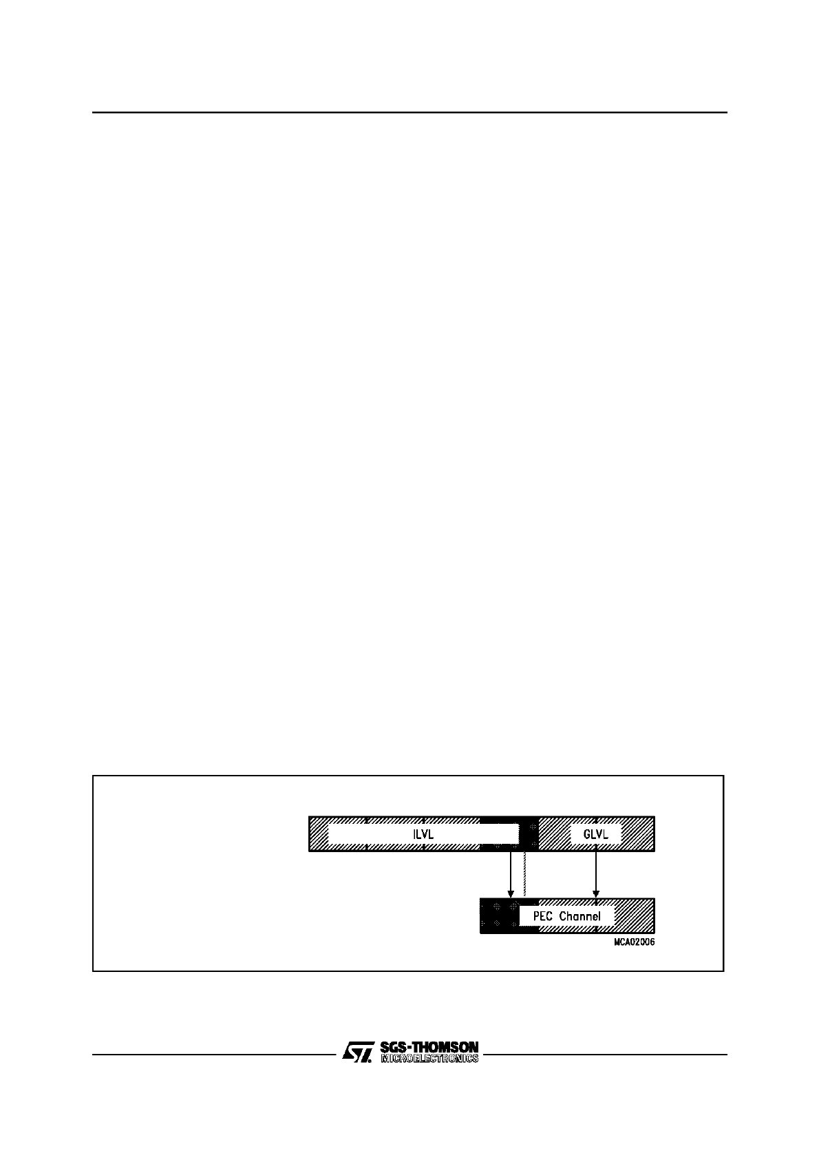
6/24
4 - INTERRUPT AND TRAP FUNCTIONS (ST10R163)
INTERRUPT SYSTEM STRUCTURE(Cont’d)
The Interrupt Request Flag is set by hardware
whenever a service request from the respective
source occurs. It is cleared automatically upon en-
try into the interrupt service routine or upon a PEC
service. In the case of PEC service the Interrupt
Request flag remains set, if the COUNT field in
register PECCx of the selected PEC channel dec-
rements to zero. This allows a normal CPU inter-
rupt to respond to a completed PEC block trans-
fer.
Note: Modifying the Interrupt Request flag via software
causes the same effects as if it had been set or
cleared by hardware.
Interrupt Priority Level and Group Level
The four bits of bit field ILVL specify the priority
level of a service request for the arbitration of si-
multaneous requests. The priority increases with
the numerical value of ILVL, so 0000b is the low-
est and 1111b is the highest priority level.
When more than one interrupt request on a specif-
ic level becomes active at the same time, the val-
ues in the respective bit fields GLVL are used for
second level arbitration to select one request for
being serviced. Again the group priority increases
with the numerical value of GLVL, so 00b is the
lowest and 11b is the highest group priority.
Note: All interrupt request sources that are enabled and
programmed to the same priority level must always
be programmed to different group priorities. Other-
wise an incorrect interrupt vector will be generated.
Upon entry into the interrupt service routine, the
priority level of the source that won the arbitration
and who’s priority level is higher than the current
CPU level, is copied into bit field ILVL of register
PSW after pushing the old PSW contents on the
stack.
The interrupt system of the ST10R163 allows
nesting of up to 15 interrupt service routines of dif-
ferent priority levels (level 0 cannot be arbitrated).
Interrupt requests that are programmed to priority
levels 15 or 14 (ie, ILVL=111Xb) will be serviced
by the PEC, unless the COUNT field of the asso-
ciated PECC register contains zero. In this case
the request will be serviced by normal interrupt
processing instead. Interrupt requests that are
programmed to priority levels 13 through 1 will al-
ways be serviced by normal interrupt processing.
Note: Priority level 0000b is the default level of the CPU.
Therefore a request on level 0 will never be serv-
iced, because it can never interrupt the CPU. How-
ever, an enabled interrupt request on level 0000b
will terminate the ST10R163’s Idle mode and reac-
tivate the CPU.
For interrupt requests which are to be serviced by
the PEC, the associated PEC channel number is
derived from the respective ILVL (LSB) and GLVL
(see figure below). So programming a source to
priority level 15 (ILVL=1111b) selects the PEC
channel group 7...4, programming a source to pri-
ority level 14 (ILVL=1110b) selects the PEC chan-
nel group 3...0. The actual PEC channel number is
then determined by the group priority field GLVL.
Simultaneous requests for PEC channels are pri-
oritized according to the PEC channel number,
where channel 0 has lowest and channel 7 has
highest priority.
Note: All sources that request PEC service must be pro-
grammed to different PEC channels. Otherwise an
incorrect PEC channel may be activated.
Figure 4-1. Priority Levels and PEC Channels
Interrupt
Control Register
PEC Control
58

7/24
4 - INTERRUPT AND TRAP FUNCTIONS (ST10R163)
INTERRUPT SYSTEM STRUCTURE(Cont’d)
The table below shows in a few examples, which action is executed with a given programming of an in-
terrupt control register.
Note: All requests on levels 13...1 cannot initiate PEC transfers. They are always serviced by an interrupt service routine.
No PECC register is associated and no COUNT field is checked.
Interrupt Control Functions in the PSW
The Processor Status Word (PSW) is functionally
divided into 2 parts: the lower byte of the PSW ba-
sically represents the arithmetic status of the
CPU, the upper byte of the PSW controls the inter-
rupt system of the ST10R163 and the arbitration
mechanism for the external bus interface.
Note: Pipeline effects have to be considered when ena-
bling/disabling interrupt requests via modifications of
register PSW (see chapter “The Central Processing
Unit”).
Priority Level
Type of Service
ILVL
GLVL
COUNT = 00h
COUNT
≠
00h
1 1 1 1
1 1
CPU interrupt,
level 15, group priority 3
PEC service,
channel 7
1 1 1 1
1 0
CPU interrupt,
level 15, group priority 2
PEC service,
channel 6
1 1 1 0
1 0
CPU interrupt,
level 14, group priority 2
PEC service,
channel 2
1 1 0 1
1 0
CPU interrupt,
level 13, group priority 2
CPU interrupt,
level 13, group priority 2
0 0 0 1
1 1
CPU interrupt,
level 1, group priority 3
CPU interrupt,
level 1, group priority 3
0 0 0 1
0 0
CPU interrupt,
level 1, group priority 0
CPU interrupt,
level 1, group priority 0
0 0 0 0
X X
No service!
No service!
59
8/24
4 - INTERRUPT AND TRAP FUNCTIONS (ST10R163)
INTERRUPT SYSTEM STRUCTURE(Cont’d)
PSW (FF10h / 88h)
SFR
Reset Value: 0000h
CPU Priority ILVL defines the current level for the
operation of the CPU. This bit field reflects the pri-
ority level of the routine that is currently executed.
Upon the entry into an interrupt service routine this
bit field is updated with the priority level of the re-
quest that is being serviced. The PSW is saved on
the system stack before. The CPU level deter-
mines the minimum interrupt priority level that will
be serviced. Any request on the same or a lower
level will not be acknowledged.
The current CPU priority level may be changed via
software to control which interrupt request sourc-
es will be acknowledged.
PEC transfers do not really interrupt the CPU, but
rather “steal” a single cycle, so PEC services do
not influence the ILVL field in the PSW.
Hardware traps switch the CPU level to maximum
priority (ie. 15) so no interrupt or PEC requests will
be acknowledged while an exception trap service
routine is executed.
Note: The TRAP instruction does not change the CPU
level, thus software invoked trap service routines
may be interrupted by higher requests.
Interrupt Enable bit IENglobally enables or disa-
bles PEC operation and the acceptance of inter-
rupts by the CPU. When IEN is cleared, no inter-
rupt requests are accepted by the CPU. When IEN
is set to ’1’, all interrupt sources, which have been
individually enabled by the interrupt enable bits in
their associated control registers, are globally en-
abled.
Note: Traps are non-maskable and are therefore not af-
fected by the IEN bit.
Bit
Function
N, C, V, Z, E,
MULIP, USR0
CPU status flags (Described in section “The Central Processing Unit”)
Define the current status of the CPU (ALU, multiplication unit).
HLDEN
HOLD Enable (Enables External Bus Arbitration)
0: Bus arbitration disabled, P6.7...P6.5 may be used for general purpose IO
1: Bus arbitration enabled, P6.7...P6.5 serve as BREQ, HLDA, HOLD, resp.
ILVL
CPU Priority Level
Defines the current priority level for the CPU
Fh: Highest priority level
0h: Lowest priority level
IEN
Interrupt Enable Control Bit (globally enables/disables interrupt requests)
‘0’: Interrupt requests are disabled
‘1’: Interrupt requests are enabled
HLD
EN
-
MUL
IP
USR0
N
Z
C
V
E
5
4
3
2
1
0
11
10
9
8
7
6
15
14
13
12
rw
rw
rw
rw
-
rw
rw
rw
-
rw
-
rw
IEN
-
-
ILVL
rw
60
9/24
4 - INTERRUPT AND TRAP FUNCTIONS (ST10R163)
4.2 OPERATION OF THE PEC CHANNELS
The ST10R163’s Peripheral Event Controller
(PEC) provides 8 PEC service channels, which
move a single byte or word between two locations
in segment 0 (data pages 3...0). This is the fastest
possible interrupt response and in many cases is
sufficient to service the respective peripheral re-
quest (eg. serial channels, etc.). Each channel is
controlled by a dedicated PEC Channel Coun-
ter/Control register (PECCx) and a pair of pointers
for source (SRCPx) and destination (DSTPx) of
the data transfer.
The PECC registers control the action that is per-
formed by the respective PEC channel.
PECCx (FECyh / 6zh, see table)
SFR
Reset Value: 0000h
PEC Control Register Addresses
Byte/Word Transfer bit BWTcontrols, if a byte or
a word is moved during a PEC service cycle. This
selection controls the transferred data size and
the increment step for the modified pointer.
Bit
Function
COUNT
PEC Transfer Count
Counts PEC transfers and influences the channel’s action (see table below)
BWT
Byte / Word Transfer Selection
0: Transfer a Word
1: Transfer a Byte
INC
Increment Control (Modification of SRCPx or DSTPx)
0 0: Pointers are not modified
0 1: Increment DSTPx by 1 or 2 (BWT)
1 0: Increment SRCPx by 1 or 2 (BWT)
1 1: Reserved. Do not use this combination. (changed to 10 by hardware)
Register
Address
Reg. Space
Register
Address
Reg. Space
PECC0
FEC0h / 60h
SFR
PECC4
FEC8h / 64h
SFR
PECC1
FEC2h / 61h
SFR
PECC5
FECAh / 65h
SFR
PECC2
FEC4h / 62h
SFR
PECC6
FECCh / 66h
SFR
PECC3
FEC6h / 63h
SFR
PECC7
FECEh / 67h
SFR
-
-
5
4
3
2
1
0
11
10
9
8
7
6
15
14
13
12
rw
rw
rw
-
BWT
-
-
-
-
-
-
-
INC
COUNT
61
10/24
4 - INTERRUPT AND TRAP FUNCTIONS (ST10R163)
OPERATION OF THE PEC CHANNELS(Cont’d)
Increment Control Field INC specifies if one of
the PEC pointers is incremented after the PEC
transfer. It is not possible to increment both point-
ers, however. If the pointers are not modified
(INC=00), the respective channel will always
move data from the same source to the same des-
tination.
Note: The reserved combination 11 is changed to 10 by
hardware. However, it is not recommended to use
this combination.
The PEC Transfer Count Field COUNTcontrols
the action of a respective PEC channel, where the
content of bit field COUNT at the time the request
is activated selects the action. COUNT may allow
a specified number of PEC transfers, unlimited
transfers or no PEC service at all.
The table below summarizes, how the COUNT
field itself, the interrupt requests flag IR and the
PEC channel action depends on the previous con-
tent of COUNT.
The PEC transfer counter allows to service a
specified number of requests by the respective
PEC channel, and then (when COUNT reaches
00h) activate the interrupt service routine, which is
associated with the priority level. After each PEC
transfer the COUNT field is decremented and the
request flag is cleared to indicate that the request
has been serviced.
Note: After PEC Service
Continuous transfers are selected by the value
FFh in bit field COUNT. In this case COUNT is not
modified and the respective PEC channel services
any request until it is disabled again.
When COUNT is decremented from 01h to 00h af-
ter a transfer, the request flag is not cleared, which
generates another request from the same source.
When COUNT already contains the value 00h, the
respective PEC channel remains idle and the as-
sociated interrupt service routine is activated in-
stead. This allows to choose, if a level 15 or 14 re-
quest is to be serviced by the PEC or by the inter-
rupt service routine.
Note: PEC transfers are only executed, if their priority lev-
el is higher than the CPU level, ie. only PEC chan-
nels 7...4 are processed, while the CPU executes
on level 14.
All interrupt request sources that are enabled and
programmed for PEC service should use different
channels. Otherwise only one transfer will be per-
formed
for
all
simultaneous
requests.
When
COUNT is decremented to 00h, and the CPU is to
be interrupted, an incorrect interrupt vector will be
generated.
COUNT
COUNT
(1)
IR after PEC
service
Action of PEC Channel and Comments
FFh
FFh
‘0’
Move a Byte / Word
Continuous transfer mode, ie. COUNT is not modified
FEh..02h
FDh..01h
‘0’
Move a Byte / Word and decrement COUNT
01h
00h
‘1’
Move a Byte / Word
Leave request flag set, which triggers another request
00h
00h
‘1’
No action!
Activate interrupt service routine rather than PEC channel.
62
11/24
4 - INTERRUPT AND TRAP FUNCTIONS (ST10R163)
OPERATION OF THE PEC CHANNELS(Cont’d)
The source and destination pointers specifiy
the locations between which the data is to be
moved. A pair of pointers (SRCPx and DSTPx) is
associated with each of the 8 PEC channels.
These pointers do not reside in specific SFRs, but
are mapped into
the internal RAM of the
ST10R163 just below the bit-addressable area
(see figure below).
PEC data transfers do not use the data page
pointers DPP3...DPP0. The PEC source and des-
tination pointers are used as 16-bit intra-segment
addresses within segment 0, so that data can be
transferred between any two locations within the
first four data pages 3...0.
The pointer locations for inactive PEC channels
may be used for general data storage. Only the re-
quired pointers occupy RAM locations.
Note: If word data transfer is selected for a specific PEC
channel (ie. BWT=’0’), the respective source and
destination pointers must both contain a valid word
address which points to an even byte boundary.
Otherwise the Illegal Word Access trap will be in-
voked, when this channel is used.
Figure 1-2. Mapping of PEC Pointers into the Internal RAM
DSTP7
00’FCFEh
SRCP7
00’FCFCh
DSTP6
00’FCFAh
SRCP6
00’FCF8h
DSTP5
00’FCF6h
SRCP5
00’FCF4h
DSTP4
00’FCF2h
SRCP4
00’FCF0h
DSTP3
00’FCEEh
SRCP3
00’FCECh
DSTP2
00’FCEAh
SRCP2
00’FCE8h
DSTP1
00’FCE6h
SRCP1
00’FCE4h
DSTP0
00’FCE2h
SRCP0
00’FCE0h
RAM
RAM
Address
Address
63

12/24
4 - INTERRUPT AND TRAP FUNCTIONS (ST10R163)
4.3 PRIORITIZATION OF INTERRUPT AND PEC SERVICE REQUESTS
Interrupt and PEC service requests from all sourc-
es can be enabled, so they are arbitrated and
serviced (if chosen), or they may be disabled, so
their requests are disregarded and not serviced.
Enabling and disabling interrupt requestsmay
be done via three mechanisms:
Control Bits allow to switch each individual
source “ON” or “OFF”, so it may generate a re-
quest or not. The control bits (xxIE) are located in
the respective interrupt control registers. All inter-
rupt requests may be enabled or disabled general-
ly via bit IEN in register PSW. This control bit is the
“main switch” that selects, if requests from any
source are accepted or not.
For a specific request to be arbitrated the respec-
tive source’s enable bit and the global enable bit
must both be set.
The Priority Level automatically selects a certain
group of interrupt requests that will be acknowl-
edged, disclosing all other requests. The priority
level of the source that won the arbitration is com-
pared against the CPU’s current level and the
source is only serviced, if its level is higher than
the current CPU level. Changing the CPU level to
a specific value via software blocks all requests on
the same or a lower level. An interrupt source that
is assigned to level 0 will be disabled and never be
serviced.
The ATOMIC and EXTend instructions auto-
matically disable all interrupt requests for the du-
ration of the following 1...4 instructions. This is
useful eg. for semaphore handling and does not
require to re-enable the interrupt system after the
unseparable instruction sequence (see chapter
“System Programming”).
Interrupt Class Management
An interrupt class covers a set of interrupt sources
with the same importance, ie. the same priority
from the system’s viewpoint. Interrupts of the
same class must not interrupt each other. The
ST10R163 supports this function with two fea-
tures:
Classes with up to 4 members can be established
by using the same interrupt priority (ILVL) and as-
signing a dedicated group level (GLVL) to each
member. This functionality is built-in and handled
automatically by the interrupt controller.
Classes with more than 4 members can be estab-
lished by using a number of adjacent interrupt pri-
orities (ILVL) and the respective group levels (4
per ILVL). Each interrupt service routine within this
class sets the CPU level to the highest interrupt
priority within the class. All requests from the
same or any lower level are blocked now, ie. no
request of this class will be accepted.
The example below establishes 3 interrupt class-
es which cover 2 or 3 interrupt priorities, depend-
ing on the number of members in a class. A level 6
interrupt disables all other sources in class 2 by
changing the current CPU level to 8, which is the
highest priority (ILVL) in class 2. Class 1 requests
or PEC requests are still serviced in this case.
The 24 interrupt sources (excluding PEC re-
quests) are so assigned to 3 classes of priority
rather than to 7 different levels, as the hardware
support would do.
64
13/24
4 - INTERRUPT AND TRAP FUNCTIONS (ST10R163)
PRIORITIZATION OF INTERRUPT AND PEC SERVICE REQUESTS(Cont’d)
Software controlled Interrupt Classes (Example)
ILVL
(Priority)
GLVL
Interpretation
3
2
1
0
15
PEC service on up to 8 channels
14
13
12
X
X
X
X
Interrupt Class 1
8 sources on 2 levels
11
X
X
X
X
10
9
8
X
X
X
X
Interrupt Class 2
10 sources on 3 levels
7
X
X
X
X
6
X
X
5
X
X
X
X
Interrupt Class 3
6 sources on 2 levels
4
X
X
3
2
1
0
No service!
65
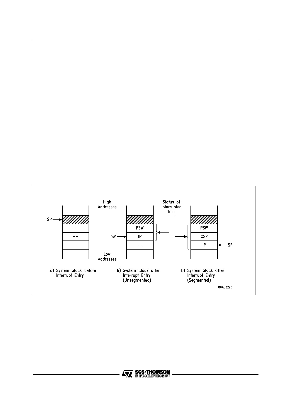
14/24
4 - INTERRUPT AND TRAP FUNCTIONS (ST10R163)
4.4 SAVING THE STATUS DURING INTERRUPT SERVICE
Before an interrupt request that has been arbitrat-
ed is actually serviced, the status of the current
task is automatically saved on the system stack.
The CPU status (PSW) is saved along with the lo-
cation, where the execution of the interrupted task
is to be resumed after returning from the service
routine. This return location is specified through
the Instruction Pointer (IP) and, in case of a seg-
mented memory model, the Code Segment Point-
er (CSP). Bit SGTDIS in register SYSCON con-
trols, how the return location is stored.
The system stack receives the PSW first, followed
by the IP (unsegmented) or followed by CSP and
then IP (segmented mode). This optimizes the us-
age of the system stack, if segmentation is disa-
bled.
The CPU priority field (ILVL in PSW) is updated
with the priority of the interrupt request that is to be
serviced, so the CPU now executes on the new
level. If a multiplication or division was in progress
at the time the interrupt request was acknowl-
edged, bit MULIP in register PSW is set to ‘1’. In
this case the return location that is saved on the
stack is not the next instruction in the instruction
flow, but rather the multiply or divide instruction it-
self, as this instruction has been interrupted and
will be completed after returning from the service
routine.
The interrupt request flag of the source that is be-
ing serviced is cleared. The IP is loaded with the
vector associated with the requesting source (the
CSP is cleared in case of segmentation) and the
first instruction of the service routine is fetched
from the respective vector location, which is ex-
pected to branch to the service routine itself. The
data page pointers and the context pointer are not
affected.
When the interrupt service routine is left (RETI is
executed), the status information is popped from
the system stack in the reverse order, taking into
account
the
value
of
bit
SGTDIS.
Figure 1-3. Task Status saved on the System Stack
66

15/24
4 - INTERRUPT AND TRAP FUNCTIONS (ST10R163)
4.5 SAVING THE STATUS DURING INTERRUPT
SERVICE
Context Switching
An interrupt service routine usually saves all the
registers it uses on the stack, and restores them
before returning. The more registers a routine us-
es, the more time is wasted with saving and re-
storing. The ST10R163 allows to switch the com-
plete bank of CPU registers (GPRs) with a single
instruction, so the service routine executes within
its own, separate context.
The instruction “SCXT CP, #New_Bank” pushes
the content of the context pointer (CP) on the sys-
tem stack and loads CP with the immediate value
“New_Bank”, which selects a new register bank.
The service routine may now use its “own regis-
ters”. This register bank is preserved, when the
service routine terminates, ie. its contents are
available on the next call.
Before returning (RETI) the previous CP is simply
POPped from the system stack, which returns the
registers to the original bank.
Note: The first instruction following the SCXT instruction
must not use a GPR.
Resources that are used by the interrupting pro-
gram must eventually be saved and restored, eg.
the DPPs and the registers of the MUL/DIV unit.
4.6 INTERRUPT RESPONSE TIMES
The interrupt response time defines the time from
an interrupt request flag of an enabled interrupt
source being set until the first instruction (I1) being
fetched from the interrupt vector location. The ba-
sic interrupt response time for the ST10R163 is 3
instruction cycles.
All instructions in the pipeline including instruction
N (during which the interrupt request flag is set)
are completed before entering the service routine.
The actual execution time for these instructions
(eg. waitstates) therefore influences the interrupt
response time.
In the figure below the respective interrupt request
flag is set in cycle 1 (fetching of instruction N). The
indicated source wins the prioritization round (dur-
ing cycle 2). In cycle 3 a TRAP instruction is inject-
ed into the decode stage of the pipeline, replacing
instruction N+1 and clearing the source’s interrupt
request flag to ’0’. Cycle 4 completes the injected
TRAP instruction (save PSW, IP and CSP, if seg-
mented mode) and fetches the first instruction (I1)
from the respective vector location.
All instructions that entered the pipeline after set-
ting of the interrupt request flag (N+1, N+2) will be
executed after returning from the interrupt service
routine.
The minimum interrupt response time is 5 states
(250 ns @ 20 MHz CPU clock). This requires pro-
gram execution with the fastest bus configuration
(16-bit, demultiplexed, no wait states), no external
operand read requests and setting the interrupt re-
quest flag during the last state of an instruction cy-
cle. When the interrupt request flag is set during
the first state of an instruction cycle, the minimum
interrupt response time under these conditions is
6 state times (300 ns @ 20 MHz CPU clock).
The interrupt response time is increased by all de-
lays of the instructions in the pipeline that are exe-
cuted before entering the service routine (includ-
ing N).
67
16/24
4 - INTERRUPT AND TRAP FUNCTIONS (ST10R163)
4.7 INTERRUPT RESPONSE TIMES
Figure 1-4. Pipeline Diagram for Interrupt Response Time
•
When internal hold conditions between instruc-
tion pairs N-2/N-1 or N-1/N occur, or instruction N
explicitly writes to the PSW or the SP, the mini-
mum interrupt response time may be extended by
1 state time for each of these conditions.
•
In case instruction N reads the PSW and instruc-
tion N-1 has an effect on the condition flags, the
interrupt response time may additionally be ex-
tended by 2 state times.
Any reference to external locations increases the
interrupt response time due to pipeline related ac-
cess priorities. The following conditions have to be
considered:
•
Instruction fetch from an external location
•
Operand read from an external location
•
Result write-back to an external location
Depending on where the instructions, source and
destination operands are located, there are a
number of combinations. Note, however, that only
access conflicts contribute to the delay.
A few examples illustrate these delays:
•
The worst case interrupt response time including
external accesses will occur, when instructions N,
N+1 and N+2 are executed out of external memo-
ry, instructions N-1 and N require external oper-
and read accesses, instructions N-3 through N
write back external operands, and the interrupt
vector also points to an external location. In this
case the interrupt response time is the time to per-
form 9 word bus accesses, because instruction I1
cannot be fetched via the external bus until all
write, fetch and read requests of preceding in-
structions in the pipeline are terminated.
•
When instructions N, N+1 and N+2 are executed
out of external memory and the interrupt vector
also points to an external location, but all oper-
ands for instructions N-3 through N are in internal
memory, then the interrupt response time is the
time to perform 3 word bus accesses.
After an interrupt service routine has been termi-
nated by executing the RETI instruction, and if fur-
ther interrupts are pending, the next interrupt serv-
ice routine will not be entered until at least two in-
struction cycles have been executed of the pro-
gram that was interrupted. In most cases two in-
structions will be executed during this time. Only
one instruction will typically be executed, if the first
instruction following the RETI instruction is a
branch instruction (without cache hit) or if it is exe-
cuted out of the internal RAM.
Note: A bus access in this context also includes delays
caused by an external READY signal or by bus ar-
bitration (HOLD mode).
Pipeline Stage
Cycle 1
Cycle 2
Cycle 3
Cycle 4
FETCH
N
N + 1
N + 2
I1
DECODE
N - 1
N
TRAP (1)
TRAP (2)
EXECUTE
N - 2
N - 1
N
TRAP
WRITEBACK
N - 3
N - 2
N - 1
N
Interrupt Response Time
1
0
IR-Flag
68
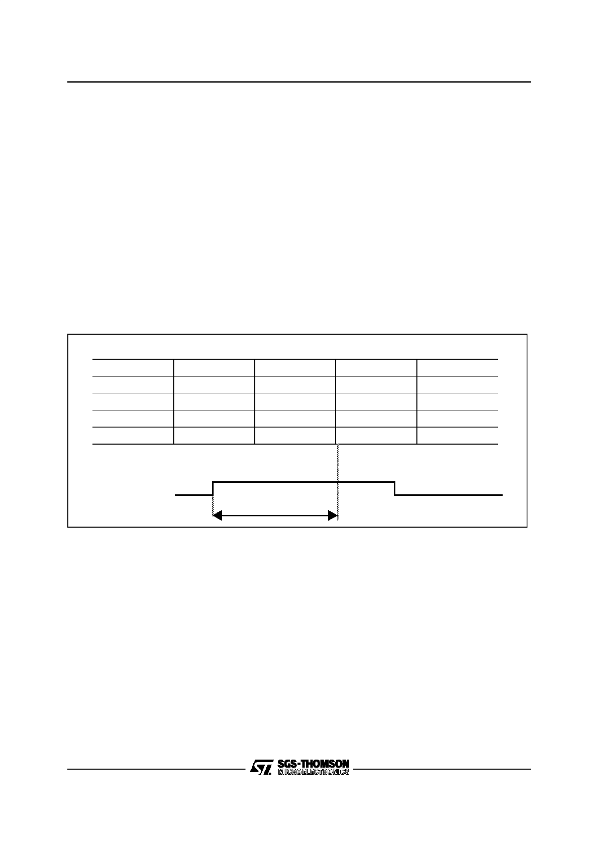
17/24
4 - INTERRUPT AND TRAP FUNCTIONS (ST10R163)
INTERRUPT RESPONSE TIMES (Cont’d)
4.7.1 PEC Response Times
The PEC response time defines the time from an
interrupt request flag of an enabled interrupt
source being set until the PEC data transfer being
started. The basic PEC response time for the
ST10R163 is 2 instruction cycles.
In the figure below the respective interrupt request
flag is set in cycle 1 (fetching of instruction N). The
indicated source wins the prioritization round (dur-
ing cycle 2). In cycle 3 a PEC transfer “instruction”
is injected into the decode stage of the pipeline,
suspending instruction N+1 and clearing the
source’s interrupt request flag to ’0’. Cycle 4 com-
pletes the injected PEC transfer and resumes the
execution of instruction N+1.
All instructions that entered the pipeline after set-
ting of the interrupt request flag (N+1, N+2) will be
executed after the PEC data transfer.
Note: When instruction N reads any of the PEC control
registers PECC7...PECC0, while a PEC request
wins the current round of prioritization, this round is
repeated and the PEC data transfer is started one
cycle later.
The minimum PEC response time is 3 states (150
ns @ 20 MHz CPU clock). This requires program
execution with the fastest bus configuration (16-
bit, demultiplexed, no wait states), no external op-
erand read requests and setting the interrupt re-
quest flag during the last state of an instruction cy-
cle. When the interrupt request flag is set during
the first state of an instruction cycle, the minimum
PEC response time under these conditions is 4
state times (200 ns @ 20 MHz CPU clock).
Figure 1-5. Pipeline Diagram for PEC Response Time
Pipeline Stage
Cycle 1
Cycle 2
Cycle 3
Cycle 4
FETCH
N
N + 1
N + 2
N + 2
DECODE
N - 1
N
PEC
N + 1
EXECUTE
N - 2
N - 1
N
PEC
WRITEBACK
N - 3
N - 2
N - 1
N
PEC Response Time
1
0
IR-Flag
69

18/24
4 - INTERRUPT AND TRAP FUNCTIONS (ST10R163)
INTERRUPT RESPONSE TIMES (Cont’d)
The PEC response time is increased by all delays
of the instructions in the pipeline that are executed
before starting the data transfer (including N).
•
When internal hold conditions between instruc-
tion pairs N-2/N-1 or N-1/N occur, the minimum
PEC response time may be extended by 1 state
time for each of these conditions.
•
In case instruction N reads the PSW and instruc-
tion N-1 has an effect on the condition flags, the
PEC response time may additionally be extended
by 2 state times.
Any reference to external locations increases the
PEC response time due to pipeline related access
priorities. The following conditions have to be con-
sidered:
•
Instruction fetch from an external location
•
Operand read from an external location
•
Result write-back to an external location
Depending on where the instructions, source and
destination operands are located, there are a
number of combinations. Note, however, that only
access conflicts contribute to the delay.
A few examples illustrate these delays:
•
The worst case interrupt response time including
external accesses will occur, when instructions N
and N+1 are executed out of external memory, in-
structions N-1 and N require external operand
read accesses and instructions N-3, N-2 and N-1
write back external operands. In this case the PEC
response time is the time to perform 7 word bus
accesses.
•
When instructions N and N+1 are executed out
of external memory, but all operands for instruc-
tions N-3 through N-1 are in internal memory, then
the PEC response time is the time to perform 1
word bus access plus 2 state times.
Once a request for PEC service has been ac-
knowledged by the CPU, the execution of the next
instruction is delayed by 2 state times plus the ad-
ditional time it might take to fetch the source oper-
and from external memory and to write the desti-
nation operand over the external bus in an exter-
nal program environment.
Note: A bus access in this context also includes delays
caused by an external READY signal or by bus ar-
bitration (HOLD mode).
70

19/24
4 - INTERRUPT AND TRAP FUNCTIONS (ST10R163)
4.8 EXTERNAL INTERRUPTS
Although the ST10R163 has no dedicated INTR
input pins, it provides many possibilities to react
on external asynchronous events by using a
number of IO lines for interrupt input. The interrupt
function may either be combined with the pin’s
main function or may be used instead of it, ie. if the
main pin function is not required.
Interrupt signals may be connected to:
•
T4IN, T2IN, the timer input pins,
•
CAPIN, the capture input of GPT2
For each of these pins either a positive, a nega-
tive, or both a positive and a negative external
transition can be selected to cause an interrupt or
PEC service request. The edge selection is per-
formed in the control register of the peripheral de-
vice associated with the respective port pin. The
peripheral must be programmed to a specific op-
erating mode to allow generation of an interrupt by
the external signal. The priority of the interrupt re-
quest is determined by the interrupt control regis-
ter of the respective peripheral interrupt source,
and the interrupt vector of this source will be used
to service the external interrupt request.
Note: In order to use any of the listed pins as external in-
terrupt input, it must be switched to input mode via
its direction control bit DPx.y in the respective port
direction control register DPx.
Pins T2IN or T4IN can be used as external inter-
rupt input pins when the associated auxiliary timer
T2 or T4 in block GPT1 is configured for capture
mode. This mode is selected by programming the
mode control fields T2M or T4M in control regis-
ters T2CON or T4CON to 101b. The active edge
of the external input signal is determined by bit
fields T2I or T4I. When these fields are pro-
grammed to X01b, interrupt request flags T2IR or
T4IR in registers T2IC or T4IC will be set on a pos-
itive external transition at pins T2IN or T4IN, re-
spectively. When T2I or T4I are programmed to
X10b, then a negative external transition will set
the corresponding request flag. When T2I or T4I
are programmed to X11b, both a positive and a
negative transition will set the request flag. In all
three cases, the contents of the core timer T3 will
be captured into the auxiliary timer registers T2 or
T4 based on the transition at pins T2IN or T4IN.
When the interrupt enable bits T2IE or T4IE are
set, a PEC request or an interrupt request for vec-
tor T2INT or T4INT will be generated.
Pin CAPIN differs slightly from the timer input pins
as it can be used as external interrupt input pin
without affecting peripheral functions. When the
capture mode enable bit T5SC in register T5CON
is cleared to ’0’, signal transitions on pin CAPIN
will only set the interrupt request flag CRIR in reg-
ister CRIC, and the capture function of register
CAPREL is not activated.
So register CAPREL can still be used as reload
register for GPT2 timer T5, while pin CAPIN
serves as external interrupt input. Bit field CI in
register T5CON selects the effective transition of
the external interrupt input signal. When CI is pro-
grammed to 01b, a positive external transition will
set the interrupt request flag. CI=10b selects a
negative transition to set the interrupt request flag,
and with CI=11b, both a positive and a negative
transition will set the request flag. When the inter-
rupt enable bit CRIE is set, an interrupt request for
vector CRINT or a PEC request will be generated.
Note: The non-maskable interrupt input pin NMI and the
reset input RSTIN provide another possibility for the
CPU to react on an external input signal. NMI and
RSTIN are dedicated input pins, which cause hard-
ware traps.
Pins to be used as External Interrupt Inputs
Port Pin
Origi nal Functio n
Control Register
P3.7/T2IN
Auxiliary timer T2 input pin
T2CON
P3.5/T4IN
Auxiliary timer T4 input pin
T4CON
P3.2/CAPIN
GPT2 capture input pin
T5CON
71
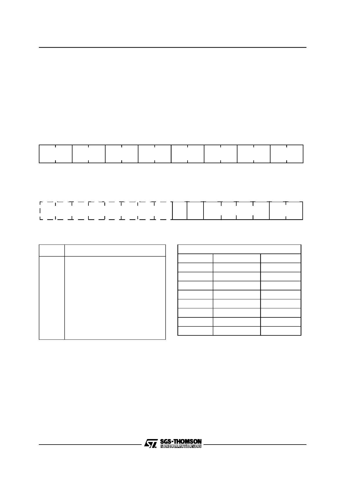
20/24
4 - INTERRUPT AND TRAP FUNCTIONS (ST10R163)
EXTERNAL INTERRUPTS (Cont’d)
Fast External Interrupts
The input pins that may be used for external inter-
rupts are sampled every 400 ns (@ 20 MHz CPU
clock), ie. external events are scanned and detect-
ed in timeframes of 400 ns. The ST10R163 pro-
vides 8 interrupt inputs that are sampled every 50
ns (@ 20 MHz CPU clock), so external events are
captured faster than with standard interrupt inputs.
The pins of Port 2 (EX0IN-EX7IN on P2.8-P2.15)
can individually be programmed to this fast inter-
rupt mode, where also the trigger transition (rising,
falling or both) can be selected. The External In-
terrupt Control register EXICON controls this fea-
ture for all 8 pins.
EXICON (F1C0h / E0h)
ESFR
Reset Value: 0000h
CCxIC (See Table)
SFR
Reset Value: --00h
Note: The fast external interrupt inputs are sampled every
50 ns. The interrupt request
arbitration
and
processing, however, is executed every 200 ns
(both @ 20 MHz CPU clock).
Note: Please refer to the general interrupt control register
description for an explanation of the control fields.
5
4
3
2
1
0
11
10
9
8
7
6
15
14
13
12
rw
rw
rw
EXI2ES
EXI0ES
EXI1ES
rw
rw
rw
EXI7ES
EXI5ES
EXI6ES
rw
rw
EXI3ES
EXI4ES
5
4
3
2
1
0
11
10
9
8
7
6
15
14
13
12
rw
rw
rw
CCx
IE
GLVL
-
-
-
rw
-
CCx
IR
-
-
-
-
ILVL
Bit
Function
EXIxES
External Interrupt x Edge Selection Field
(x=7...0)
0 0: Fast external interrupts disabled:
standard mode
0 1: Interrupt on positive edge (rising)
1 0: Interrupt on negative edge (falling)
1 1: Interrupt on any edge (rising or falling)
External Interrupt Control Registers
Register
Address
Reg. Space
CC8IC
FF88h/C4h
SFR
CC9IC
FF8Ah/C5h
SFR
CC10IC
FF8Ch/C6h
SFR
CC11IC
FF8Eh/C7h
SFR
CC12IC
FF90h/C8h
SFR
CC13IC
FF92h/C9h
SFR
CC14IC
FF94h/CAh
SFR
CC15IC
FF96h/CBh
SFR
72

21/24
4 - INTERRUPT AND TRAP FUNCTIONS (ST10R163)
4.9 TRAP FUNCTIONS
Traps interrupt the current execution similar to
standard interrupts. However, trap functions offer
the possibility to bypass the interrupt system’s pri-
oritization process in cases where immediate sys-
tem reaction is required. Trap functions are not
maskable and always have priority over interrupt
requests on any priority level.
The ST10R163 provides two different kinds of
trapping mechanisms. Hardware traps are trig-
gered by events that occur during program execu-
tion (eg. illegal access or undefined opcode),soft-
ware traps are initiated via an instruction within
the current execution flow.
Software Traps
The TRAP instruction is used to cause a software
call to an interrupt service routine. The trap
number that is specified in the operand field of the
trap instruction determines which vector location
in the address range from 00’0000h through
00’01FCh will be branched to.
Executing a TRAP instruction causes a similar ef-
fect as if an interrupt at the same vector had oc-
curred. PSW, CSP (in segmentation mode), and
IP are pushed on the internal system stack and a
jump is taken to the specified vector location.
When segmentation is enabled and a trap is exe-
cuted, the CSP for the trap service routine is set to
code segment 0. No Interrupt Request flags are
affected by the TRAP instruction. The interrupt
service routine called by a TRAP instruction must
be terminated with a RETI (return from interrupt)
instruction to ensure correct operation.
Note: The CPU level in register PSW is not modified by
the TRAP instruction, so the service routine is exe-
cuted on the same priority level from which it was in-
voked. Therefore, the service routine entered by the
TRAP instruction can be interrupted by other traps
or higher priority interrupts, other than when trig-
gered by a hardware trap.
Hardware Traps
Hardware traps are issued by faults or specific
system states that occur during runtime of a pro-
gram (not identified at assembly time). A hardware
trap may also be triggered intentionally, eg. to em-
ulate additional instructions by generating an Ille-
gal Opcode trap. The ST10R163 distinguishes
eight different hardware trap functions. When a
hardware trap condition has been detected, the
CPU branches to the trap vector location for the
respective trap condition. Depending on the trap
condition, the instruction which caused the trap is
either completed or cancelled (ie. it has no effect
on the system state) before the trap handling rou-
tine is entered.
Hardware traps are non-maskable and always
have priority over every other CPU activity. If sev-
eral hardware trap conditions are detected within
the same instruction cycle, the highest priority trap
is serviced (see table in section “Interrupt System
Structure”).
PSW, CSP (in segmentation mode), and IP are
pushed on the internal system stack and the CPU
level in register PSW is set to the highest possible
priority level (ie. level 15), disabling all interrupts.
The CSP is set to code segment zero, if segmen-
tation is enabled. A trap service routine must be
terminated with the RETI instruction.
The
eight
hardware
trap
functions
of
the
ST10R163 are divided into two classes:
Class A traps are
•
external Non-Maskable Interrupt (NMI)
•
Stack Overflow
•
Stack Underflow trap
These traps share the same trap priority, but have
an individual vector address.
Class B traps are
•
Undefined Opcode
•
Protection Fault
•
Illegal Word Operand Access
•
Illegal Instruction Access
•
Illegal External Bus Access Trap
These traps share the same trap priority, and the
same vector address.
73

22/24
4 - INTERRUPT AND TRAP FUNCTIONS (ST10R163)
T TRAP FUNCTIONS (Cont’d)
he bit-addressable Trap Flag Register (TFR) al-
lows a trap service routine to identify the kind of
trap which caused the exception. Each trap func-
tion is indicated by a separate request flag. When
a hardware trap occurs, the corresponding re-
quest flag in register TFR is set to ’1’.
TFR (FFACh / D6h)
SFR
Reset Value: 0000h
Note: The trap service routine must clear the respective trap flag, otherwise a new trap will be requested after exiting the
service routine. Setting a trap request flag by software causes the same effects as if it had been set by hardware.
Bit
Function
ILLBUS
Illegal External Bus Access Flag
An external access has been attempted with no external bus defined.
ILLINA
Illegal Instruction Access Flag
A branch to an odd address has been attempted.
ILLOPA
Illegal Word Operand Access Flag
A word operand access (read or write) to an odd address has been attempted.
PRTFLT
Protection Fault Flag
A protected instruction with an illegal format has been detected.
UNDOPC
Undefined Opcode Flag
The currently decoded instruction has no valid ST10R163 opcode.
STKUF
Stack Underflow Flag
The current stack pointer value exceeds the content of register STKUN.
STKOF
Stack Overflow Flag
The current stack pointer value falls below the content of register STKOV.
NMI
Non Maskable Interrupt Flag
A negative transition (falling edge) has been detected on pin NMI.
NMI
5
4
3
2
1
0
11
10
9
8
7
6
15
14
13
12
rw
rw
rw
rw
rw
-
-
-
-
rw
-
-
-
STK
UF
ILL
BUS
ILL
INA
ILL
OPA
PRT
FLT
UND
OPC
STK
OF
-
-
-
-
-
-
-
-
-
rw
rw
74

23/24
4 - INTERRUPT AND TRAP FUNCTIONS (ST10R163)
T TRAP FUNCTIONS (Cont’d)
The reset functions (hardware, software, watch-
dog) may be regarded as a type of trap. Reset
functions have the highest system priority (trap
priority III).
Class A traps have the second highest priority
(trap priority II), on the 3rd rank are class B traps,
so a class A trap can interrupt a class B trap. If
more than one class A trap occur at a time, they
are prioritized internally, with the NMI trap on the
highest and the stack underflow trap on the lowest
priority.
All class B traps have the same trap priority (trap
priority I). When several class B traps get active at
a time, the corresponding flags in the TFR register
are set and the trap service routine is entered.
Since all class B traps have the same vector, the
priority of service of simultaneously occurring
class B traps is determined by software in the trap
service routine.
A class A trap occurring during the execution of a
class B trap service routine will be serviced imme-
diately. During the execution of a class A trap
service routine, however, any class B trap occur-
ring will not be serviced until the class A trap serv-
ice routine is exited with a RETI instruction. In this
case, the occurrence of the class B trap condition
is stored in the TFR register, but the IP value of
the instruction which caused this trap is lost.
In the case where e.g. an Undefined Opcode trap
(class B) occurs simultaneously with an NMI trap
(class A), both the NMI and the UNDOPC flag is
set, the IP of the instruction with the undefined op-
code is pushed onto the system stack, but the NMI
trap is executed. After return from the NMI service
routine, the IP is popped from the stack and imme-
diately pushed again because of the pending UN-
DOPC trap.
External NMI Trap
Whenever a high to low transition on the dedicat-
ed external NMI pin (Non-Maskable Interrupt) is
detected, the NMI flag in register TFR is set and
the CPU will enter the NMI trap routine. The IP val-
ue pushed on the system stack is the address of
the instruction following the one after which nor-
mal processing was interrupted by the NMI trap.
Stack Overflow Trap
Whenever the stack pointer is decremented to a
value which is less than the value in the stack
overflow register STKOV, the STKOF flag in regis-
ter TFR is set and the CPU will enter the stack
overflow trap routine. Which IP value will be
pushed onto the system stack depends on which
operation caused the decrement of the SP. When
an implicit decrement of the SP is made through a
PUSH or CALL instruction, or upon interrupt or
trap entry, the IP value pushed is the address of
the following instruction. When the SP is decre-
mented by a subtract instruction, the IP value
pushed represents the address of the instruction
after the instruction following the subtract instruc-
tion.
For recovery from stack overflow it must be en-
sured that there is enough excess space on the
stack for saving the current system state (PSW,
IP, in segmented mode also CSP) twice. Other-
wise, a system reset should be generated.
Stack Underflow Trap
Whenever the stack pointer is incremented to a
value which is greater than the value in the stack
underflow register STKUN, the STKUF flag is set
in register TFR and the CPU will enter the stack
underflow trap routine. Again, which IP value will
be pushed onto the system stack depends on
which operation caused the increment of the SP.
When an implicit increment of the SP is made
through a POP or return instruction, the IP value
pushed is the address of the following instruction.
When the SP is incremented by an add instruc-
tion, the pushed IP value represents the address
of the instruction after the instruction following the
add instruction.
Undefined Opcode Trap
When the instruction currently decoded by the
CPU does not contain a valid ST10R163 opcode,
the UNDOPC flag is set in register TFR and the
CPU enters the undefined opcode trap routine.
The IP value pushed onto the system stack is the
address of the instruction that caused the trap.
This can be used to emulate unimplemented in-
structions. The trap service routine can examine
the faulting instruction to decode operands for un-
implemented opcodes based on the stacked IP. In
order to resume processing, the stacked IP value
must be incremented by the size of the undefined
instruction, which is determined by the user, be-
fore a RETI instruction is executed.
75

24/24
4 - INTERRUPT AND TRAP FUNCTIONS (ST10R163)
T TRAP FUNCTIONS (Cont’d)
Protection Fault Trap
Whenever one of the special protected instruc-
tions is executed where the opcode of that instruc-
tion is not repeated twice in the second word of the
instruction and the byte following the opcode is not
the complement of the opcode, the PRTFLT flag in
register TFR is set and the CPU enters the protec-
tion fault trap routine. The protected instructions
include DISWDT, EINIT, IDLE, PWRDN, SRST,
and SRVWDT. The IP value pushed onto the sys-
tem stack for the protection fault trap is the ad-
dress of the instruction that caused the trap.
Illegal Word Operand Access Trap
Whenever a word operand read or write access is
attempted to an odd byte address, the ILLOPA
flag in register TFR is set and the CPU enters the
illegal word operand access trap routine. The IP
value pushed onto the system stack is the address
of the instruction following the one which caused
the trap.
Illegal Instruction Access Trap
Whenever a branch is made to an odd byte ad-
dress, the ILLINA flag in register TFR is set and
the CPU enters the illegal instruction access trap
routine. The IP value pushed onto the system
stack is the illegal odd target address of the
branch instruction.
Illegal External Bus Access Trap
Whenever the CPU requests an external instruc-
tion fetch, data read or data write, and no external
bus configuration has been specified, the ILLBUS
flag in register TFR is set and the CPU enters the
illegal bus access trap routine. The IP value
pushed onto the system stack is the address of
the instruction following the one which caused the
trap. However the ST10R165 being a romless mi-
crocontroller, an external bus must be defined and
such a trap should never occur.
76
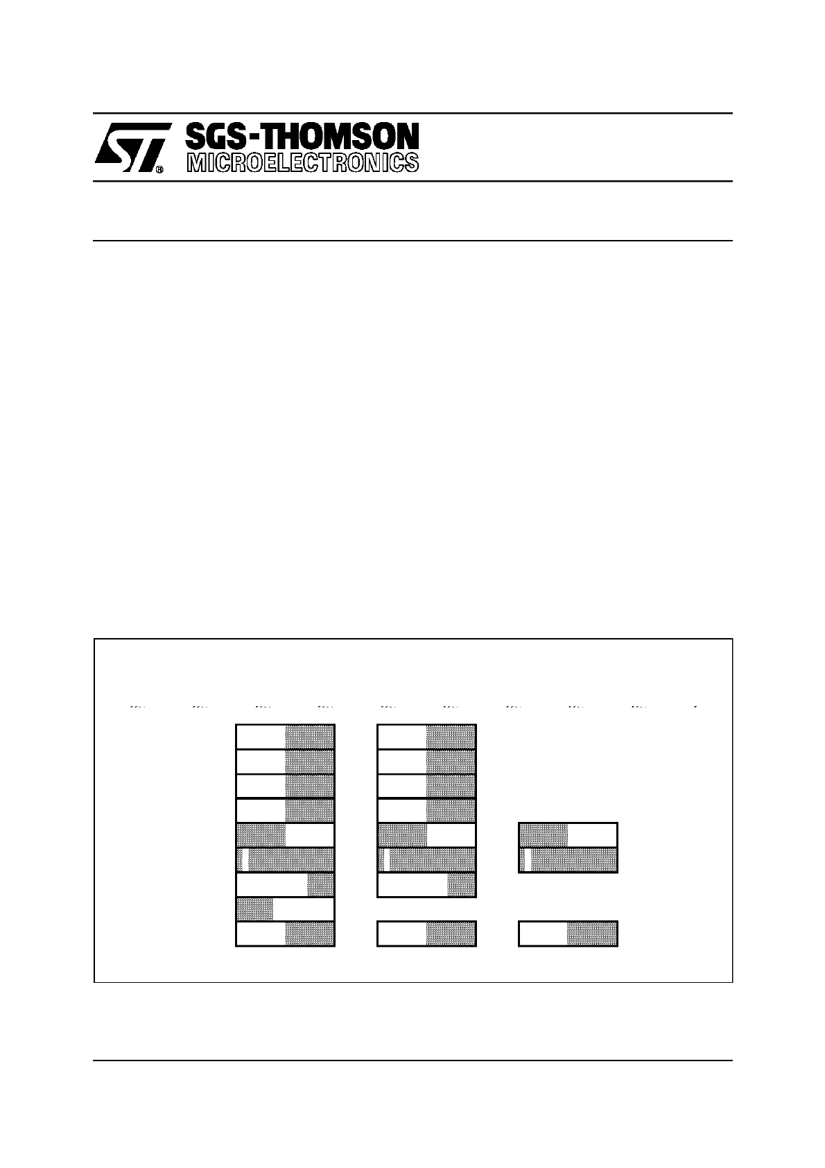
February 1996
1/28
This is advance information from SGS-TH OMSON. Details are subject tochange without notice.
ST10R163
User Manual
5 - PARALLEL PORTS
In order to accept or generate single external con-
trol signals or parallel data, the ST10R163 pro-
vides up to 77 parallel IO lines organized into sev-
en 8-bit IO ports (PORT0 made of P0H and P0L,
PORT1 made of P1H and P1L, Port 2, Port 6), one
15-bit IO port (Port 3), one 8-bit IO port (Port 4)
and one 6-bit input port (Port 5).
These port lines may be used for general purpose
Input/Output controlled via software or may be
used implicitly by ST10R163’s integrated periph-
erals or the External Bus Controller.
Using part as General Purpose I/O lines.
All port lines are bit addressable, and all input/out-
put lines are individually (bit-wise) programmable
as inputs or outputs via direction registers (except
Port 5). The IO ports are true bidirectional ports
which are switched to high impedance state when
configured as inputs. The output drivers of three
IO ports (2, 3, 6) can be configured (pin by pin) for
push/pull operation or open-drain operation via
control registers. The logic level of a pin is clocked
into the input latch once per state time, regardless
whether the port is configured for input or output.
A write operation to a port pin configured as an in-
put causes the value to be written into the port out-
put latch, while a read operation returns the
latched state of the pin itself. A read-modify-write
operation reads the value of the pin, modifies it,
and writes it back to the output latch.
Writing
to a
pin
configured
as
an
output
(DPx.y=‘1’) causes the output latch and the pin to
have the written value, since the output buffer is
enabled. Reading this pin returns the value of the
output latch. A read-modify-write operation reads
the value of the output latch, modifies it, and writes
it back to the output latch, thus also modifying the
level at the pin.
Figure 2-1. SFRs and Pins associated with the Parallel Ports
Note: E: ESFR located in the ESFR space
ODP2
E
DP2
P5
P2
Data Input / Output
Registers
Direction Control
Registers
Open Drain Control
Registers
P6
DP6
ODP6
E
P0L
P0H
DP0L
E
DP0H
E
P4
P1L
P1H
P3
DP3
DP4
DP1H
E
DP1L
E
ODP3
E
77
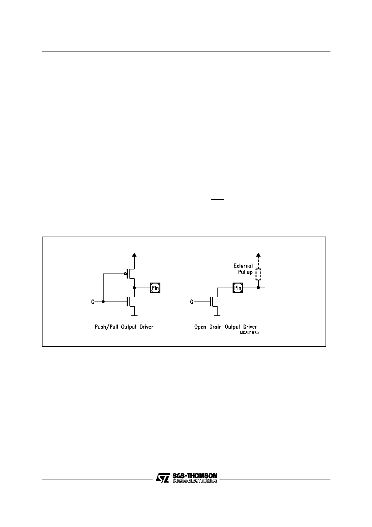
2/28
5 - PARALLEL PORTS (ST10R163)
In the ST10R163 certain ports provide Open Drain
Control, which allows to switch the output driver of
a port pin from a push/pull configuration to an
open drain configuration. In push/pull mode a port
output driver has an upper and a lower transistor,
thus it can actively drive the line either to a high or
a low level. In open drain mode the upper transis-
tor is always switched off, and the output driver
can only actively drive the line to a low level. When
writing a ‘1’ to the port latch, the lower transistor is
switched off and the output enters a high-imped-
ance state. The high level must then be provided
by an external pullup device. With this feature, it is
possible to connect several port pins together to a
Wired-AND configuration, saving external glue
logic and/or additional software overhead for ena-
bling/disabling output signals.
This feature is implemented for ports P2, P3 and
P6 (see respective sections), and is controlled
through the respective Open Drain Control Regis-
ters ODPx. These registers allow the individual
bit-wise selection of the open drain mode for each
port line. If the respective control bit ODPx.y is ‘0’
(default after reset), the output driver is in the
push/pull mode. If ODPx.y is ‘1’, the open drain
configuration is selected. Note that all ODPx reg-
isters are located in the ESFR space.
Each port line has one programmable alternate in-
put or output function associated with it.
Each port line has one programmable alternate in-
put or output function associated with it.
PORT0 and PORT1 may be used as the address
and data lines when accessing external memory.
Port 4 outputs the additional segment address bits
A23/19/17...A16 in systems where more than 64
KBytes of memory are to be accessed directly.
Port 6 provides the optional chip select outputs
and the bus arbitration lines.
Port 2 is used for fast external interrupt inputs.
Port 3 includes alternate input/output functions of
timers, serial interface, the optional bus control
signal BHE and the system clock output (CLK-
OUT).
Port 5 is used for timer control signals.
Figure 2-2. Output Drivers in Push/Pull Mode and in Open Drain Mode
78

3/28
5 - PARALLEL PORTS (ST10R163)
Alternate Input or Output function of Port
If an alternate output function of a pin is to be
used, the direction of this pin must be pro-
grammed for output (DPx.y=‘1’), except for some
signals that are used directly after reset and are
configured automatically. Otherwise the pin re-
mains in the high-impedance state and is not af-
fected by the alternate output function. The re-
spective port latch should hold a ‘1’, because its
output is ANDed with the alternate output data.
If an alternate input function of a pin is used, the
direction of the pin must be programmed for input
(DPx.y=‘0’) if an external device is driving the pin.
The input direction is the default after reset. If no
external device is connected to the pin, however,
one can also set the direction for this pin to output.
In this case, the pin reflects the state of the port
output latch. Thus, the alternate input function
reads the value stored in the port output latch.
This can be used for testing purposes to allow a
software trigger of an alternate input function by
writing to the port output latch.
On most of the port lines, the user software is re-
sponsible for setting the proper direction when us-
ing an alternate input or output function of a pin.
This is done by setting or clearing the direction
control bit DPx.y of the pin before enabling the al-
ternate function. There are port lines, however,
where the direction of the port line is switched au-
tomatically. For instance, in the multiplexed exter-
nal bus modes of PORT0, the direction must be
switched several times for an instruction fetch in
order to output the addresses and to input the da-
ta. Obviously, this cannot be done through instruc-
tions. In these cases, the direction of the port line
is switched automatically by hardware if the alter-
nate function of such a pin is enabled.
To determine the appropriate level of the port out-
put latches check how the alternate data output is
combined with the respective port latch output.
There is one basic structure for all port lines with
only an alternate input function. Port lines with
only an alternate output function, however, have
different structures due to the way the direction of
the pin is switched and depending on whether the
pin is accessible by the user software or not in the
alternate function mode.
All port lines that are not used for these alternate
functions may be used as general purpose IO
lines. When using port pins for general purpose
output, the initial output value should be written to
the port latch prior to enabling the output drivers,
in order to avoid undesired transitions on the out-
put pins. This applies to single pins as well as to
pin groups (see examples below).
SINGLE _BIT: BSET
P4.7
; Initia l output level is “high”
BSET
DP4.7
; Switch on the output driver
BIT_GR OUP:
BFLD H P4, #24h, #24h
; Initia l output level is “high”
BFLD H DP4, #24h, #24h
; Switch on the output drivers
Note: When using several BSET pairs to control
more pins of one port, these pairs must be sepa-
rated by instructions, which do not reference the
respective port (see “Particular Pipeline Effects” in
chapter “The Central Processing Unit”).
Each of these ports and the alternate input and
output functions are described in detail in the fol-
lowing subsections.
79
4/28
5 - PARALLEL PORTS (ST10R163)
5.1 PORT 0
The two 8-bit ports P0H and P0L represent the
higher and lower part of PORT0, respectively.
Both halves of PORT0 can be written (eg. via a
PEC transfer) without affecting the other half.
If this port is used for general purpose IO, the di-
rection of each line can be configured via the cor-
responding direction registers DP0H and DP0L.
P0L (FF00h / 80h)
SFR
Reset Value: - - 00h
P0h (FF02h / 81h)
SFR
Reset Value: - - 00h
DP0L (F100h / 80h)
ESFR
Reset Value: - - 00h
DP0h (F102h / 81h)
ESFR
Reset Value: - - 00h
Bit
Function
P0X.y
Port data register P0H or P0L bit y
Bit
Fun ction
DP0X.y
Port direction register DP0H or DP0L bit y
DP0X.y = 0: Port line P0X.y is an input (high-impedance)
DP0X.y = 1: Port line P0X.y is an output
5
4
3
2
1
0
11
10
9
8
7
6
15
14
13
12
rw
rw
rw
rw
rw
rw
-
-
-
-
rw
rw
-
-
-
-
P0L.0
P0L.1
P0L.2
P0L.3
P0L.4
P0L.5
P0L.6
P0L.7
5
4
3
2
1
0
11
10
9
8
7
6
15
14
13
12
rw
rw
rw
rw
rw
rw
-
-
-
-
rw
rw
-
-
-
-
P0H.0
P0H.1
P0H.2
P0H.3
P0H.4
P0H.5
P0H.6
P0H.7
5
4
3
2
1
0
11
10
9
8
7
6
15
14
13
12
rw
rw
rw
rw
rw
rw
-
-
-
-
rw
rw
-
-
-
-
DP0L
.7
DP0L
.6
DP0L
.5
DP0L
.4
DP0L
.3
DP0L
.2
DP0L
.1
DP0L
.0
5
4
3
2
1
0
11
10
9
8
7
6
15
14
13
12
rw
rw
rw
rw
rw
rw
-
-
-
-
rw
rw
-
-
-
-
DP0H
.7
DP0H
.6
DP0H
.5
DP0H
.4
DP0H
.3
DP0H
.2
DP0H
.1
DP0H
.0
80
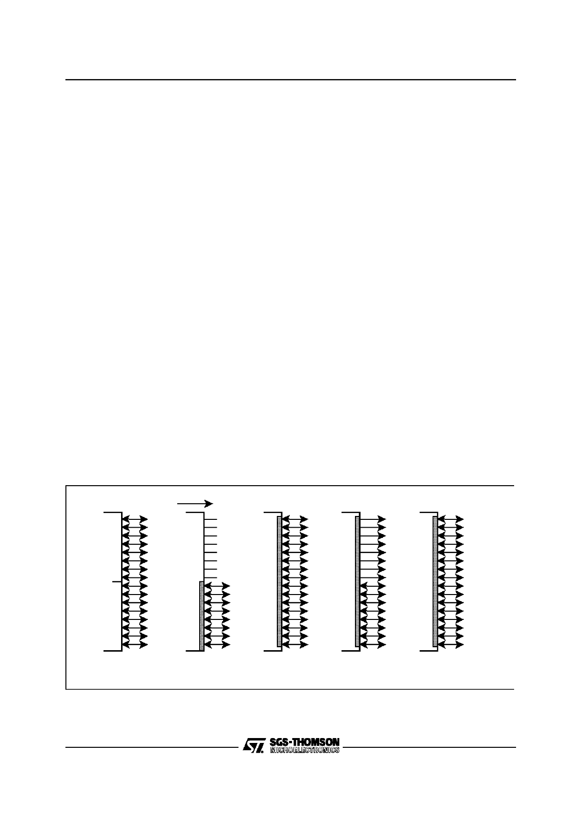
5/28
5 - PARALLEL PORTS (ST10R163)
PORT 0 (Cont’d)
5.1.1 Alternate Functions of PORT0
When an external bus is enabled, PORT0 is used
as data bus or address/data bus.
Note that an external 8-bit demultiplexed bus only
uses P0L, while P0H is free for IO (provided that
no other bus mode is enabled).
PORT0 is also used to select the system startup
configuration. During reset, PORT0 is configured
to input, and each line is held high through an in-
ternal pullup device. Each line can then be individ-
ually pulled to a low level (see DC-level specifica-
tions in the respective Data Sheets) through an
external pulldown device. A default configuration
is selected when the respective PORT0 lines are
at a high level. Through pulling individual lines to a
low level, this default can be changed according to
the needs of the applications.
The internal pullup devices are designed such that
an external pulldown resistors (see Data Sheet
specification) can be used to apply a correct low
level. These external pulldown resistors can re-
main connected to the PORT0 pins also during
normal operation, however, care has to be taken
such that they do not disturb the normal function of
PORT0 (this might be the case, for example, if the
external resistor is too strong).
With the end of reset, the selected bus configura-
tion will be written to the BUSCON0 register. The
configuration of the high byte of PORT0, will be
copied into the special register RP0H. This read-
only register holds the selection for the number of
chip selects and segment addresses. Software
can read this register in order to react according to
the selected configuration, if required.
When the reset is terminated, the internal pullup
devices are switched off, and PORT0 will be
switched to the appropriate operating mode.
During external accesses in multiplexed bus
modes PORT0 first outputs the 16-bit intra-seg-
ment address as an alternate output function.
PORT0 is then switched to high-impedance input
mode to read the incoming instruction or data. In
8-bit data bus mode, two memory cycles are re-
quired for word accesses, the first for the low byte
and the second for the high byte of the word. Dur-
ing write cycles PORT0 outputs the data byte or
word after outputting the address.
During external accesses in demultiplexed bus
modes PORT0 reads the incoming instruction or
data word or outputs the data byte or word.
Figure 2-3. PORT0 IO and Alternate Functions
P0H.7
P0H.6
P0H.5
P0H.4
P0H.3
P0H.2
P0H.1
P0H.0
P0L.7
P0L.6
P0L.5
P0L.4
P0L.3
P0L.2
P0L.1
P0L.0
PORT0
D7
D6
D5
D4
D3
D2
D1
D0
P0H
P0L
D15
D14
D13
D12
D11
D10
D9
D8
D7
D6
D5
D4
D3
D2
D1
D0
AD15
AD14
AD13
AD12
AD11
AD10
AD9
AD8
AD7
AD6
AD5
AD4
AD3
AD2
AD1
AD0
AD15
AD14
AD13
AD12
AD11
AD10
AD9
AD8
AD7
AD6
AD5
AD4
AD3
AD2
AD1
AD0
Alternate Fun ction
a)
b)
c)
d)
General Purpose
Inpu t/Outp ut
8-bit
Demux Bus
16-bit
Demux Bus
8-bit
MUX Bus
16-bit
MUX Bus
81
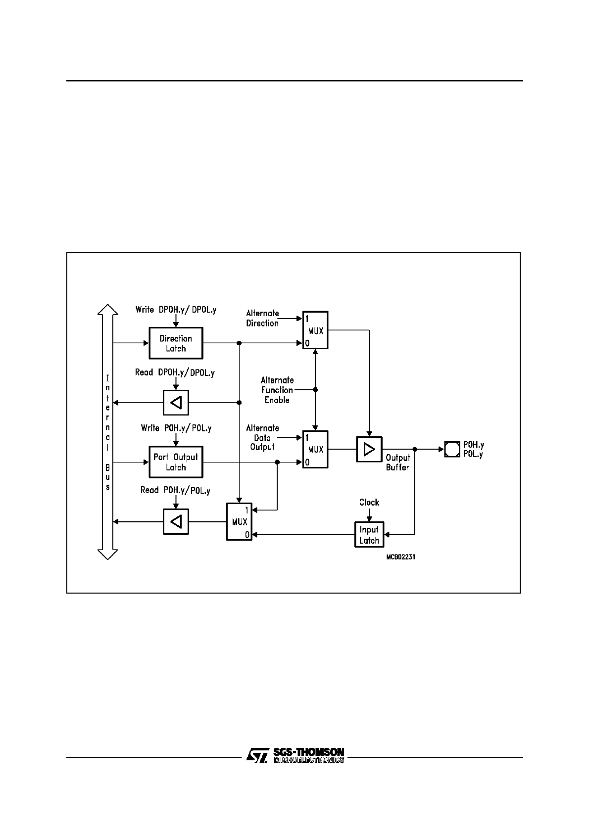
6/28
5 - PARALLEL PORTS (ST10R163)
PORT 0 (Cont’d)
When an external bus mode is enabled, the direc-
tion of the port pin and the loading of data into the
port output latch are controlled by the bus control-
ler hardware. The input of the port output latch is
disconnected
from the internal
bus
and is
switched to the line labeled “Alternate Data Out-
put” via a multiplexer. The alternate data can be
the 16-bit intrasegment address or the 8/16-bit
data information. The incoming data on PORT0 is
read on the line “Alternate Data Input”. While an
external bus mode is enabled, the user software
should not write to the port output latch, otherwise
unpredictable results may occur. When the exter-
nal bus modes are disabled, the contents of the di-
rection register last written by the user becomes
active.
The figure below shows the structure of a PORT0
pin.
Figure 2-4. Block Diagram of a PORT0 Pin
y = 7...0
82
7/28
5 - PARALLEL PORTS (ST10R163)
5.2 PORT 1
The two 8-bit ports P1H and P1L represent the
higher and lower part of PORT1, respectively.
Both halves of PORT1 can be written (eg. via a
PEC transfer) without affecting the other half.
If this port is used for general purpose IO, the di-
rection of each line can be configured via the cor-
responding direction registers DP1H and DP1L.
P1L (FF04h / 82h)
SFR
Reset Value: - - 00h
P1h (FF06h / 83h)
SFR
Reset Value: - - 00h
DP1L (F104h / 82h)
ESFR
Reset Value: - - 00h
DP1H (F106h / 83h)
ESFR
Reset Value: - - 00h
Bit
Function
P1X.y
Port data register P1H or P1L bit y
Bit
Function
DP1X.y
Port direction register DP1H or DP1L bit y
DP1X.y = 0: Port line P1X.y is an input (high-impedance)
DP1X.y = 1: Port line P1X.y is an output
5
4
3
2
1
0
11
10
9
8
7
6
15
14
13
12
rw
rw
rw
rw
rw
rw
-
-
-
-
rw
rw
-
-
-
-
P1L.0
P1L.1
P1L.2
P1L.3
P1L.4
P1L.5
P1L.6
P1L.7
5
4
3
2
1
0
11
10
9
8
7
6
15
14
13
12
rw
rw
rw
rw
rw
rw
-
-
-
-
rw
rw
-
-
-
-
P1H.0
P1H.1
P1H.2
P1H.3
P1H.4
P1H.5
P1H.6
P1H.7
5
4
3
2
1
0
11
10
9
8
7
6
15
14
13
12
rw
rw
rw
rw
rw
rw
-
-
-
-
rw
rw
-
-
-
-
DP1L
.7
DP1L
.6
DP1L
.5
DP1L
.4
DP1L
.3
DP1L
.2
DP1L
.1
DP1L
.0
5
4
3
2
1
0
11
10
9
8
7
6
15
14
13
12
rw
rw
rw
rw
rw
rw
-
-
-
-
rw
rw
-
-
-
-
DP1H
.7
DP1H
.6
DP1H
.5
DP1H
.4
DP1H
.3
DP1H
.2
DP1H
.1
DP1H
.0
83
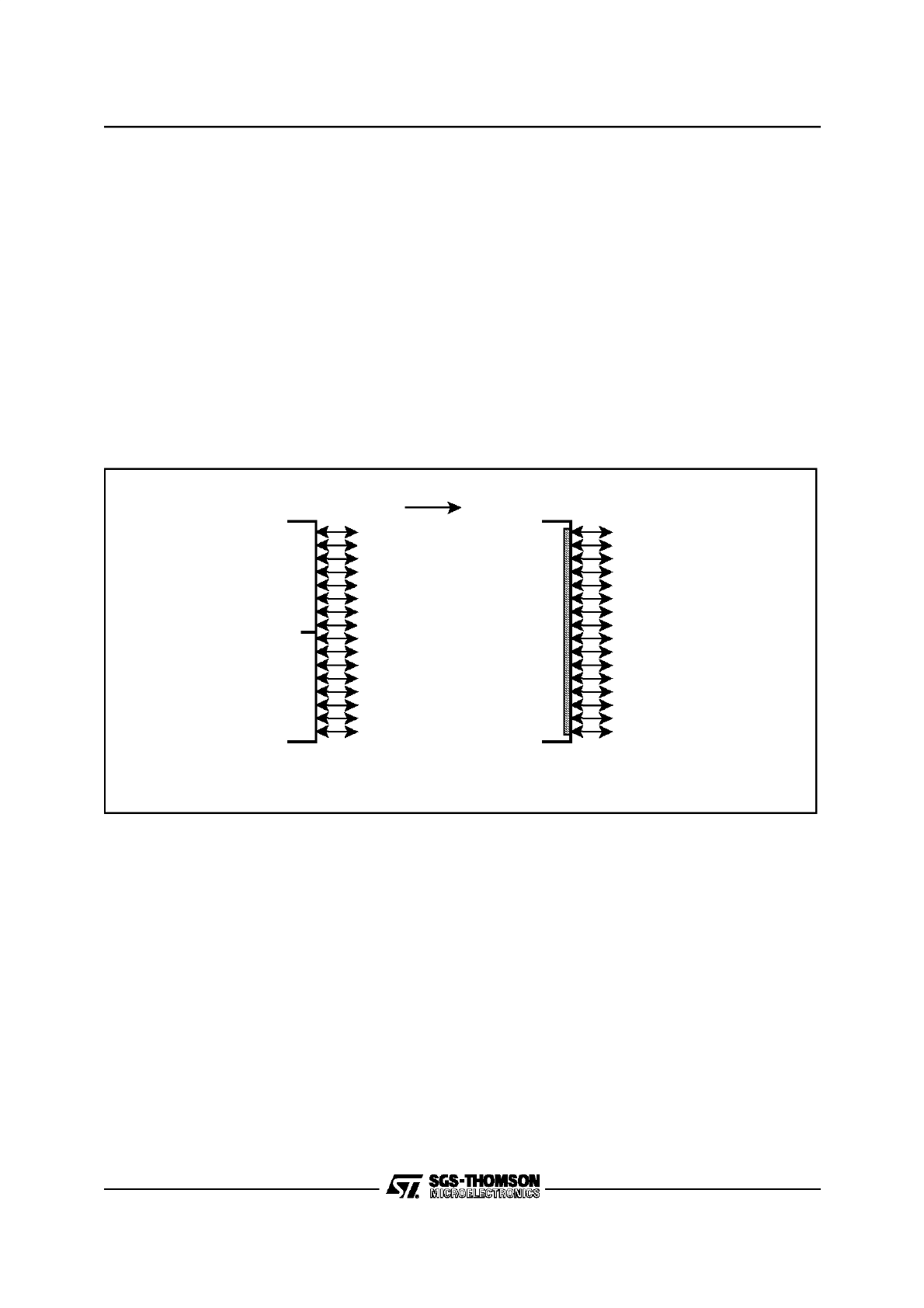
8/28
5 - PARALLEL PORTS (ST10R163)
PORT 1 (Cont’d)
5.2.1 Alternate Functions of PORT1
When a demultiplexed external bus is enabled,
PORT1 is used as address bus.
Note that demultiplexed bus modes use PORT1
as a 16-bit port. Otherwise all 16 port lines can be
used for general purpose IO.
During external accesses in demultiplexed bus
modes PORT1 outputs the 16-bit intra-segment
address as an alternate output function.
During external accesses in multiplexed bus
modes, when no BUSCON register selects a de-
multiplexed bus mode, PORT1 is not used and is
available for general purpose IO.
When an external bus mode is enabled, the direc-
tion of the port pin and the loading of data into the
port output latch are controlled by the bus control-
ler hardware. The input of the port output latch is
disconnected
from the internal
bus
and is
switched to the line labeled “Alternate Data Out-
put” via a multiplexer. The alternate data is the 16-
bit intrasegment address. While an external bus
mode is enabled, the user software should not
write to the port output latch, otherwise unpredict-
able results may occur. When the external bus
modes are disabled, the contents of the direction
register last written by the user becomes active.
Figure 2-5. PORT1 IO and Alternate Functions
P1H.7
P1H.6
P1H.5
P1H.4
P1H.3
P1H.2
P1H.1
P1H.0
P1L.7
P1L.6
P1L.5
P1L.4
P1L.3
P1L.2
P1L.1
P1L.0
PORT1
P1H
P1L
A15
A14
A13
A12
A11
A10
A9
A8
A7
A6
A5
A4
A3
A2
A1
A0
Alternate Fun ction
a)
General Purpose
Input /Output
8/16-bit
Demux Bus
84
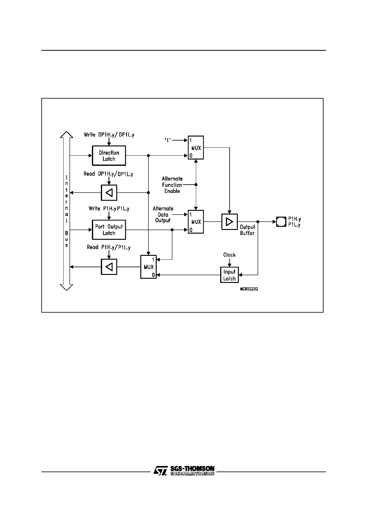
9/28
5 - PARALLEL PORTS (ST10R163)
PORT 1 (Cont’d)
The figure below shows the structure of a PORT1 pin.
Figure 2-6. Block Diagram of a PORT1 Pin
y = 7...0
85
10/28
5 - PARALLEL PORTS (ST10R163)
5.3 PORT 2
In the ST10R163 Port 2 is an 8-bit port. If Port 2 is
used for general purpose IO, the direction of each
line can be configured via the corresponding di-
rection register DP2. Each port line can be
switched into push/pull or open drain mode via the
open drain control register ODP2.
5.3.1 Alternate Functions of Port 2
All Port 2 lines (P2.15...P2.8) can serve as Fast
External Interrupt inputs (EX7IN...EX0IN).
P2 (FFC0h / E0h)
SFR
Reset Value: 00 - -h
DP2 (FFC2h / E1h)
SFR
Reset Value: 00 - -h
ODP2 (F1C2h / E1h)
ESFR
Reset Value: 00 - -h
Bit
Function
P2.y
Port data register P2 bit y
Bit
Function
DP2.y
Port direction register DP2 bit y
DP2.y = 0: Port line P2.y is an input (high-impedance)
DP2.y = 1: Port line P2.y is an output
5
4
3
2
1
0
11
10
9
8
7
6
15
14
13
12
-
-
-
-
-
-
rw
rw
rw
rw
-
-
rw
rw
rw
rw
P2.8
P2.9
P2.10
P2.11
P2.12
P2.13
P2.14
P2.15
5
4
3
2
1
0
11
10
9
8
7
6
15
14
13
12
-
-
-
-
-
-
rw
rw
rw
rw
-
-
rw
rw
rw
rw
DP2
.15
DP2
.14
DP2
.13
DP2
.12
DP2
.11
DP2
.10
DP2
.9
DP2
.8
Bit
Function
ODP2.y
Port 2 Open Drain control register bit y
ODP2.y = 0: Port line P2.y output driver in push/pull mode
ODP2.y = 1: Port line P2.y output driver in open drain mode
5
4
3
2
1
0
11
10
9
8
7
6
15
14
13
12
-
-
-
-
-
-
rw
rw
rw
rw
-
-
rw
rw
rw
rw
ODP2
.15
ODP2
.14
ODP2
.13
ODP2
.12
ODP2
.11
ODP2
.10
ODP2
.9
ODP2
.8
86
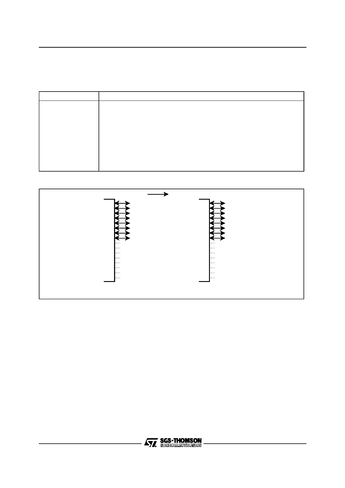
11/28
5 - PARALLEL PORTS (ST10R163)
PORT 2 (Cont’d)
The table below summarizes the alternate functions of Port 2.
Figure 2-7. Port 2 IO and Alternate Functions
Port 2 Pin
Alternate Functi on
P2.8
P2.9
P2.10
P2.11
P2.12
P2.13
P2.14
P2.15
EX0IN
Fast External Interrupt 0 Input
EX1IN
Fast External Interrupt 1 Input
EX2IN
Fast External Interrupt 2 Input
EX3IN
Fast External Interrupt 3 Input
EX4IN
Fast External Interrupt 4 Input
EX5IN
Fast External Interrupt 5 Input
EX6IN
Fast External Interrupt 6 Input
EX7IN
Fast External Interrupt 7 Input
P2.15
P2.14
P2.13
P2.12
P2.11
P2.10
P2.9
P2.8
-
-
-
-
-
-
-
-
Port 2
EX7IN
EX6IN
EX5IN
EX4IN
EX3IN
EX2IN
EX1IN
EX0IN
-
-
-
-
-
-
-
-
Alternate Functio n
a)
General Purpose
Input/Ou tput
Fast External
Interrupt Input
87
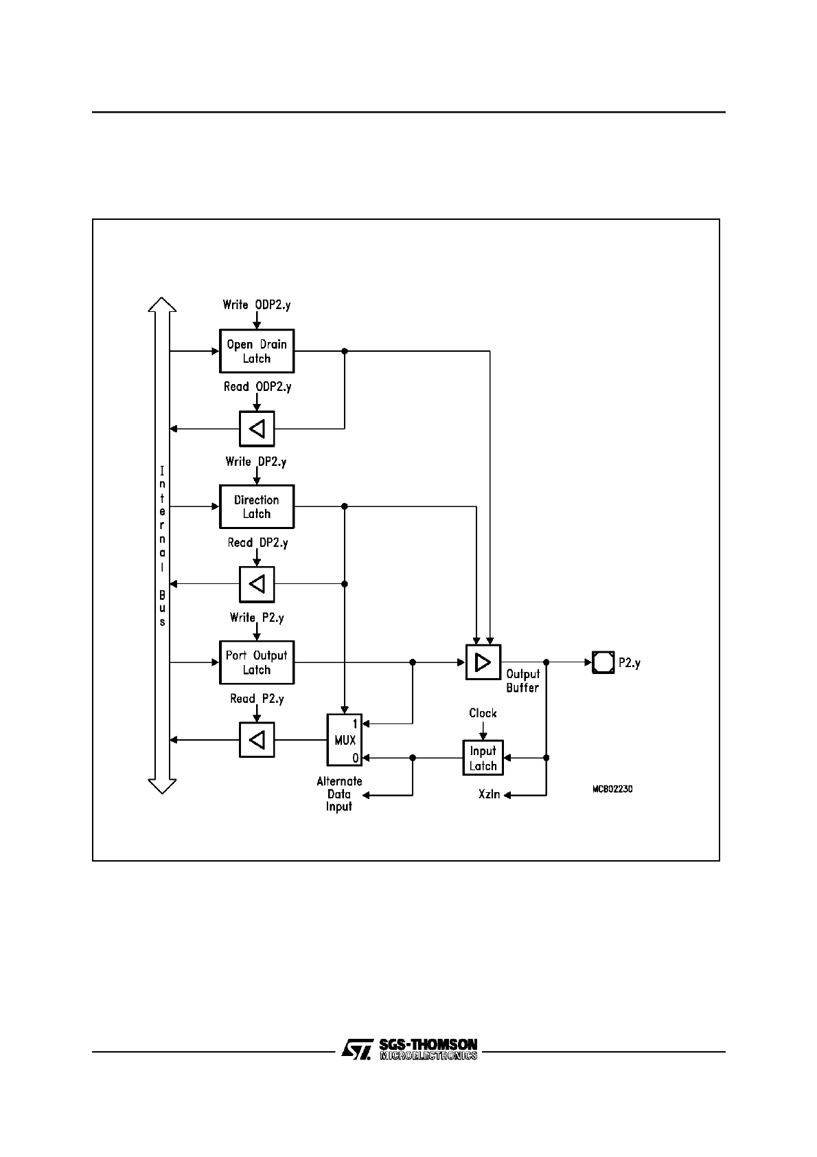
12/28
5 - PARALLEL PORTS (ST10R163)
PORT 2 (Cont’d)
The pins of Port 2 combine internal bus data and alternate data output before the port latch input.
Figure 2-8. Block Diagram of a Port 2 Pin
y = 15...8
88
13/28
5 - PARALLEL PORTS (ST10R163)
5.4 PORT 3
If this 15-bit port is used for general purpose IO,
the direction of each line can be configured via the
corresponding direction register DP3. Most port
lines can be switched into push/pull or open drain
mode via the open drain control register ODP3
(pins P3.15, P3.14 and P3.12 do not support open
drain mode!).
Due to pin limitations register bit P3.14 is not con-
nected to an output pin.
P3 (FFC4h / E2h)
SFR
Reset Value: 0000h
Note: Register bit P3.14 is not connected to an IO pin.
DP3 (FFC6h / E3h)
SFR
Reset Value: 0000h
ODP3 (F1C6h / E3h)
ESFR
Reset Value: 0000h
Bit
Function
P3.y
Port data register P3 bit y
Bit
Function
DP3.y
Port direction register DP3 bit y
DP3.y = 0: Port line P3.y is an input (high-impedance)
DP3.y = 1: Port line P3.y is an output
Bit
Function
ODP3.y
Port 3 Open Drain control register bit y
ODP3.y = 0: Port line P3.y output driver in push/pull mode
ODP3.y = 1: Port line P3.y output driver in open drain mode
5
4
3
2
1
0
11
10
9
8
7
6
15
14
13
12
rw
rw
rw
rw
rw
rw
rw
rw
rw
rw
rw
rw
rw
-
rw
rw
P3.0
P3.1
P3.2
P3.3
P3.4
P3.5
P3.6
P3.7
P3.8
P3.9
P3.10
P3.11
P3.12
P3.13
-
P3.15
-
-
-
5
4
3
2
1
0
11
10
9
8
7
6
15
14
13
12
rw
rw
rw
rw
rw
rw
rw
rw
rw
rw
rw
rw
rw
-
rw
rw
DP3
.13
DP3
.11
DP3
.10
DP3
.9
DP3
.8
DP3
.7
DP3
.6
DP3
.5
DP3
.4
DP3
.3
DP3
.2
DP3
.1
DP3
.0
-
DP3
.12
DP3
.15
-
-
-
5
4
3
2
1
0
11
10
9
8
7
6
15
14
13
12
rw
rw
rw
rw
rw
rw
rw
rw
rw
rw
rw
rw
-
-
rw
-
ODP3
.13
ODP3
.11
ODP3
.10
ODP3
.9
ODP3
.8
ODP3
.7
ODP3
.6
ODP3
.5
ODP3
.4
ODP3
.3
ODP3
.2
ODP3
.1
ODP3
.0
-
-
-
89
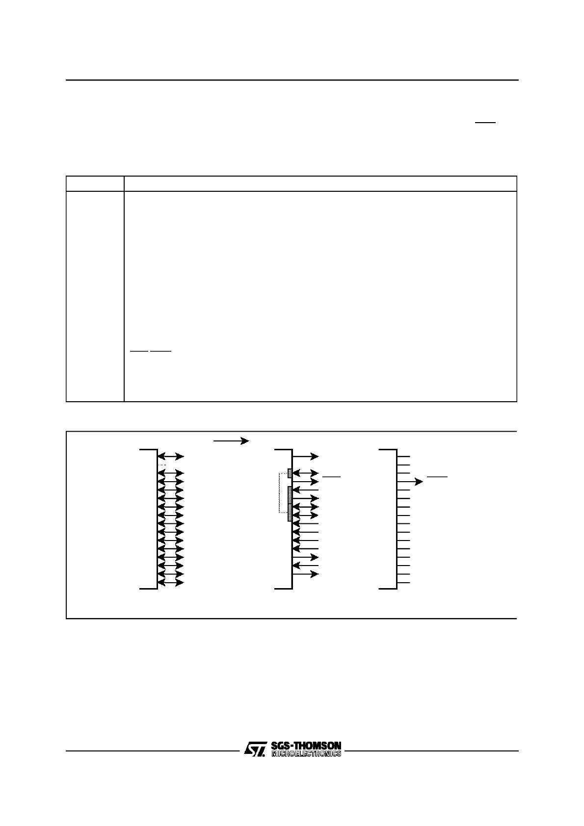
14/28
5 - PARALLEL PORTS (ST10R163)
PORT3 (Cont’d)
5.4.1 Alternate Functions of Port 3
The pins of Port 3 serve for various functions
which include external timer control lines, the two
serial interfaces and the control lines BHE and
CLKOUT.
The table below summarizes the alternate func-
tions of Port 3.
Figure 2-9. Port 3 IO and Alternate Functions
Port 3 Pin
Alternate Function
P3.0
P3.1
P3.2
P3.3
P3.4
P3.5
P3.6
P3.7
P3.8
P3.9
P3.10
P3.11
P3.12
P3.13
P3.14
P3.15
-
T6OUT
Timer 6 Toggle Output
CAPIN
GPT2 Capture Input
T3OUT
Timer 3 Toggle Output
T3EUD
Timer 3 External Up/Down Control Input
T4IN
Timer 4 Count Input
T3IN
Timer 3 Count Input
T2IN
Timer 2 Count Input
MRST
SSC Master Receive / Slave Transmit
MTSR
SSC Master Transmit / Slave Receive
TxD0
ASC0 Transmit Data Output
RxD0
ASC0 Receive Data Input
BHE/WRH
Byte High Enable / Write High Output
SCLK
SSC Shift Clock Input/Output
---
No pin assigned!
CLKOUT
System Clock Output
P3.15
P3.13
P3.12
P3.11
P3.10
P3.9
P3.8
P3.7
P3.6
P3.5
P3.4
P3.3
P3.2
P3.1
P3.0
Port 3
No Pin
CLKOUT
SCLK
BHE
RxD0
TxD0
MTSR
MRST
T2IN
T3IN
T4IN
T3EUD
T3OUT
CAPIN
T6OUT
WRH
Alternate Fun ction
a)
b)
General Purpose
Inpu t/Output
90

15/28
5 - PARALLEL PORTS (ST10R163)
PORT3 (Cont’d)
The port structure of the Port 3 pins depends on
their alternate function (see figures below).
When the on-chip peripheral associated with a
Port 3 pin is configured to use the alternate input
function, it reads the input latch, which represents
the state of the pin, via the line labeled “Alternate
Data Input”. Port 3 pins with alternate input func-
tions are:
T2IN, T3IN, T4IN, T3EUD and CAPIN.
When the on-chip peripheral associated with a
Port 3 pin is configured to use the alternate output
function, its “Alternate Data Output” line is ANDed
with the port output latch line. When using these
alternate functions, the user must set the direction
of the port line to output (DP3.y=1) and must set
the port output latch (P3.y=1). Otherwise the pin is
in its high-impedance state (when configured as
input) or the pin is stuck at ’0’ (when the port out-
put latch is cleared). When the alternate output
functions are not used, the “Alternate Data Out-
put” line is in its inactive state, which is a high level
(’1’). Port 3 pins with alternate output functions
are:
T6OUT, T3OUT, TxD0 and CLKOUT.
When the on-chip peripheral associated with a
Port 3 pin is configured to use both the alternate
input and output function, the descriptions above
apply to the respective current operating mode.
The direction must be set accordingly. Port 3 pins
with alternate input/output functions are:
MTSR, MRST, RxD0 and SCLK.
Note: Enabling the CLKOUT function automatical-
ly enables the P3.15 output driver. Setting
bit DP3.15=’1’ is not required.
91
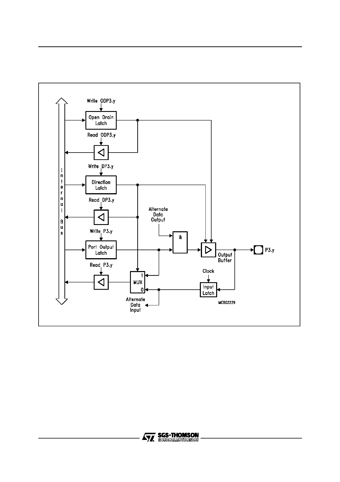
16/28
5 - PARALLEL PORTS (ST10R163)
PORT3 (Cont’d)
Figure 2-10. Block Diagram of a Port 3 Pin with Alternate Input or Alternate Output Function
y = 13, 11...0
92
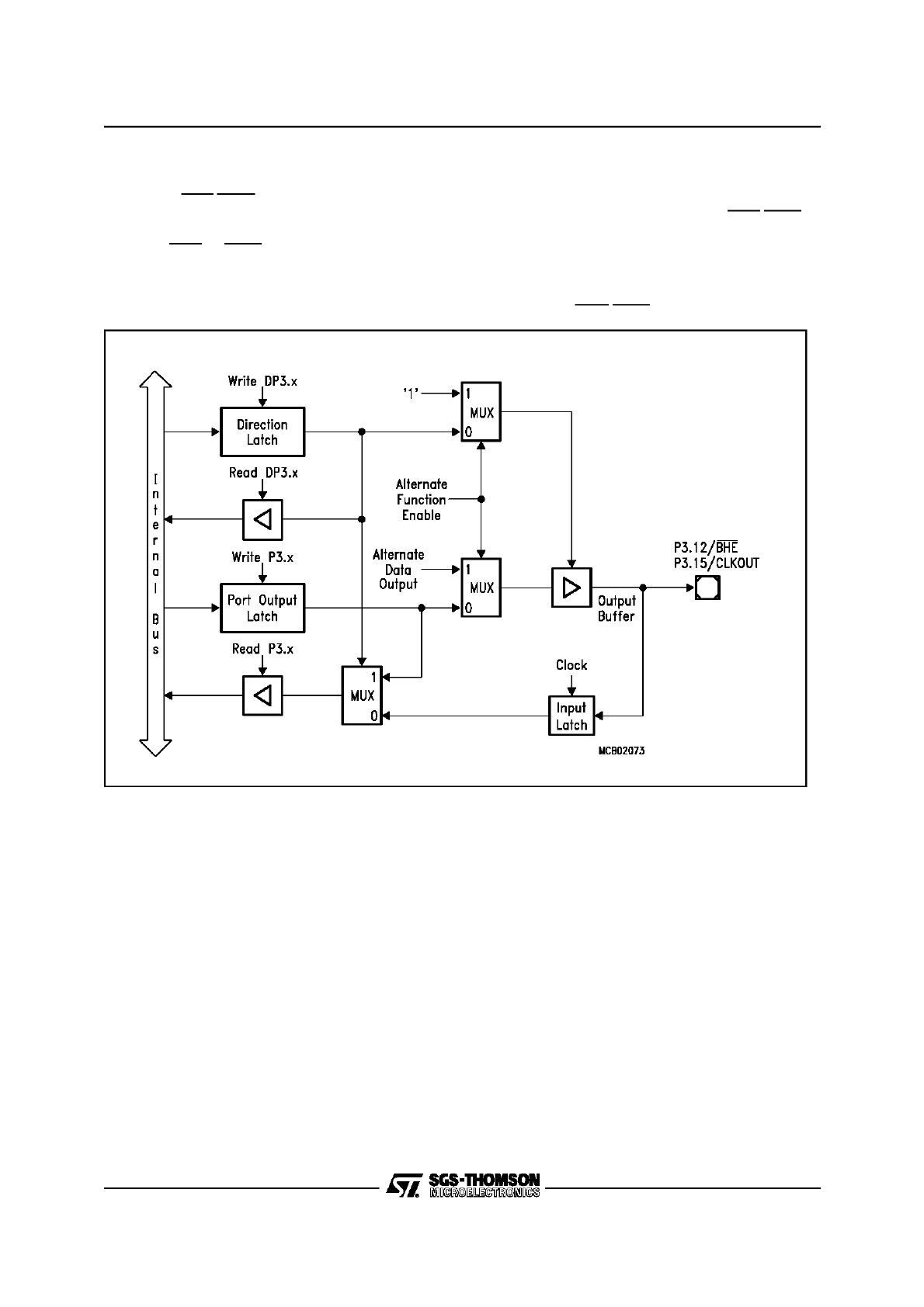
17/28
5 - PARALLEL PORTS (ST10R163)
PORT3 (Cont’d)
Pin P3.12 (BHE/WRH) is one more pin with an al-
ternate output function. However, its structure is
slightly different (see figure below), because after
reset the BHE or WRH function must be used de-
pending on the system startup configuration. In
these cases there is no possibility to program any
port latches before. Thus the appropriate alternate
function is selected automatically. IfBHE/WRH is
not used in the system, this pin can be used for
general purpose IO by disabling the alternate
function (BYTDIS = ‘1’ / WRCFG=’0’).
Figure 2-11. Block Diagram of Pins P3.15 (CLKOUT) and P3.12 (BHE/WRH)
x = 15, 12
93
18/28
5 - PARALLEL PORTS (ST10R163)
5.1 PORT 4
In the ST10R163, the Port 4 is an 8-bit port. If the
SSP is disabled (bit SSPEN cleared in SYSCON
register), Port 4 is used for general purpose IO
(the direction of each line can be configured via
the corresponding direction register DP4).
If the SSP is enabled (bit SSPEN set), the 4 upper
pins are used for the Synchronous Serial Port
(SSP) dedicated IO. The bits in the Port 4 Data
Register (P4) and the Port 4 Direction Control
Register (DP4) that correspond to the pins
SSPCLK, SSPDATA, SSPDEN0 and SSPDEN1
are no influence on these pins.
P4 (FFC8h / E4h)
SFR
Reset Value: - - 00h
DP4 (FFCAh / E5h)
SFR
Reset Value: - - 00h
Bit
Functio n
P4.y
Port data register P4 bit y
Bit
Function
DP4.y
Port direction register DP4 bit y
DP4.y = 0: Port line P4.y is an input (high-impedance)
DP4.y = 1: Port line P4.y is an output
5
4
3
2
1
0
11
10
9
8
7
6
15
14
13
12
rw
rw
rw
rw
rw
rw
-
-
-
-
rw
rw
-
-
-
-
P4.0
P4.1
P4.2
P4.3
P4.4
P4.5
P4.6
P4.7
5
4
3
2
1
0
11
10
9
8
7
6
15
14
13
12
rw
rw
rw
rw
rw
rw
-
-
-
-
rw
rw
-
-
-
-
DP4.0
DP4.1
DP4.2
DP4.3
DP4.4
DP4.5
DP4.6
DP4.7
94
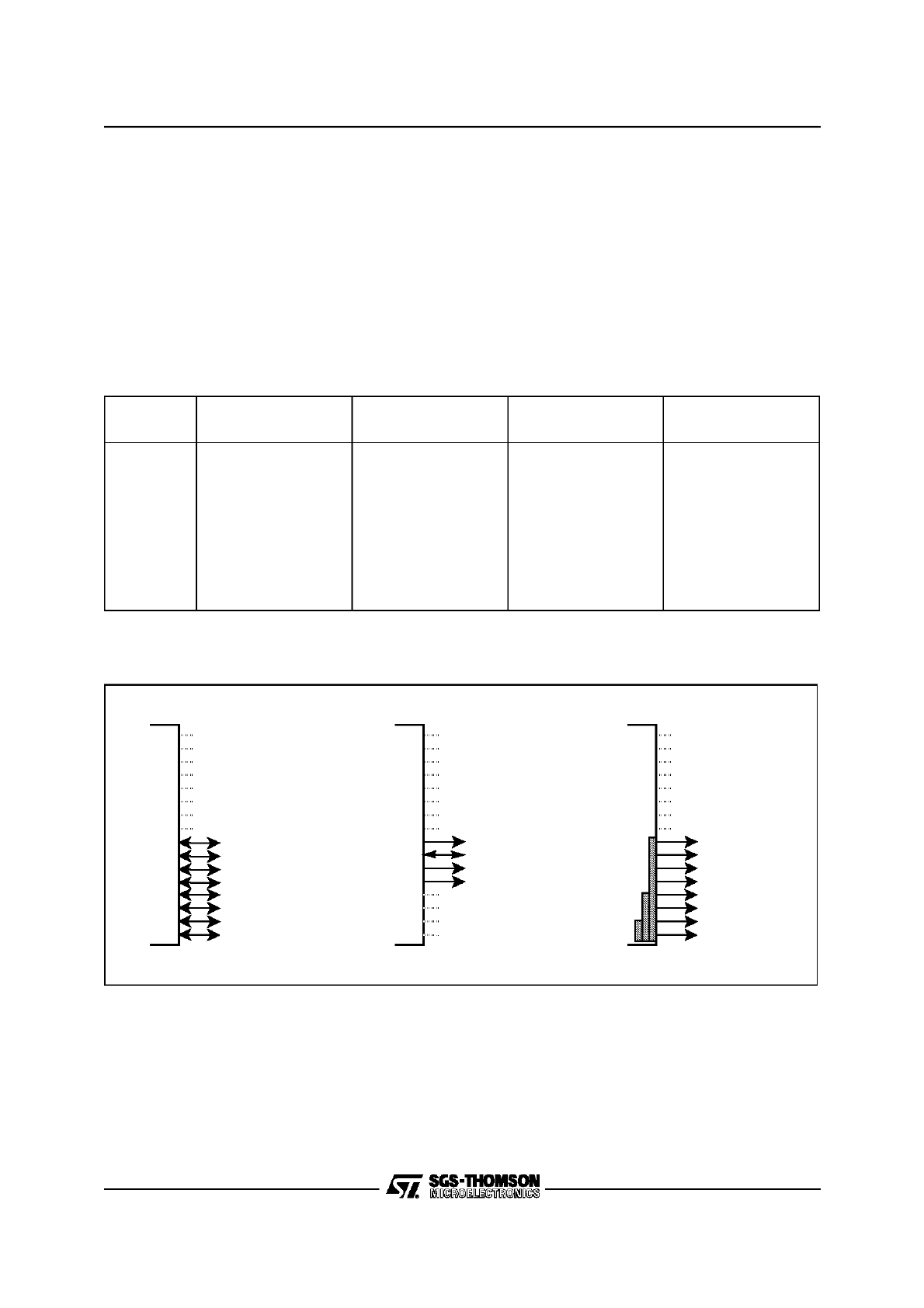
19/28
5 - PARALLEL PORTS (ST10R163)
PORT4 (Cont’d)
5.1.1 Alternate Functions of Port 4
During external bus cycles that use segmentation
(ie. an address space above 64 KByte) a number
of Port 4 pins may output the segment address
lines. The number of pins that is used for segment
address output determines the external address
space which is directly accessible. The other pins
of Port 4 (if any) may be used for general purpose
IO. If segment address lines are selected, the al-
ternate function of Port 4 may be necessary to ac-
cess eg. external memory directly after reset. For
this reason Port 4 will be switched to its alternate
function automatically.
The number of segment address lines is selected
via PORT0 during reset. The selected value can
be read from bitfield SALSEL in register RP0H
(read only) eg. in order to check the configuration
during run time.
The table below summarizes the alternate func-
tions of Port 4 depending on the number of select-
ed segment address lines (coded via bitfield SAL-
SEL) and on the state of SSPEN control bit..
Figure 2-12. Port 4 I/O and Alternate Functions
Port 4 Pin
Std. Function
SALSEL=01 64 KB
Altern. Function
SALSEL=11 256KB
Altern. Function
SALSEL=00 1 MB
Altern. Functi on
SALSEL=10 16 MB
P4.0
P4.1
P4.2
P4.3
P4.4
P4.5
P4.6
P4.7
Gen. purpose IO
Gen. purpose IO
Gen. purpose IO
Gen. purpose IO
Gen. IO / SSPCE1
Gen. IO / SSPCE0
Gen. IO / SSPDAT
Gen. IO / SSPCLK
Seg. Address A16
Seg. Address A17
Gen. purpose IO
Gen. purpose IO
Gen. IO / SSPCE1
Gen. IO / SSPCE0
Gen. IO / SSPDAT
Gen. IO / SSPCLK
Seg. Address A16
Seg. Address A17
Seg. Address A18
Seg. Address A19
Gen. IO / SSPCE1
Gen. IO / SSPCE0
Gen. IO / SSPDAT
Gen. IO / SSPCLK
Seg. Address A16
Seg. Address A17
Seg. Address A18
Seg. Address A19
Seg. Address A20
Seg. Address A21
Seg. Address A22
Seg. Address A23
-
-
-
-
-
-
-
-
P4.7
P4.6
P4.5
P4.4
P4.3
P4.2
P4.1
P4.0
Port 4
-
-
-
-
-
-
-
-
A23
A22
A21
A20
A19
A18
A17
A16
General Purpose I/O
Alternate Functio n
-
-
-
-
-
-
-
-
SSPCLK
SSPDAT
SSPCE0
SSPCE1
Port 4
Dedicated Function
95
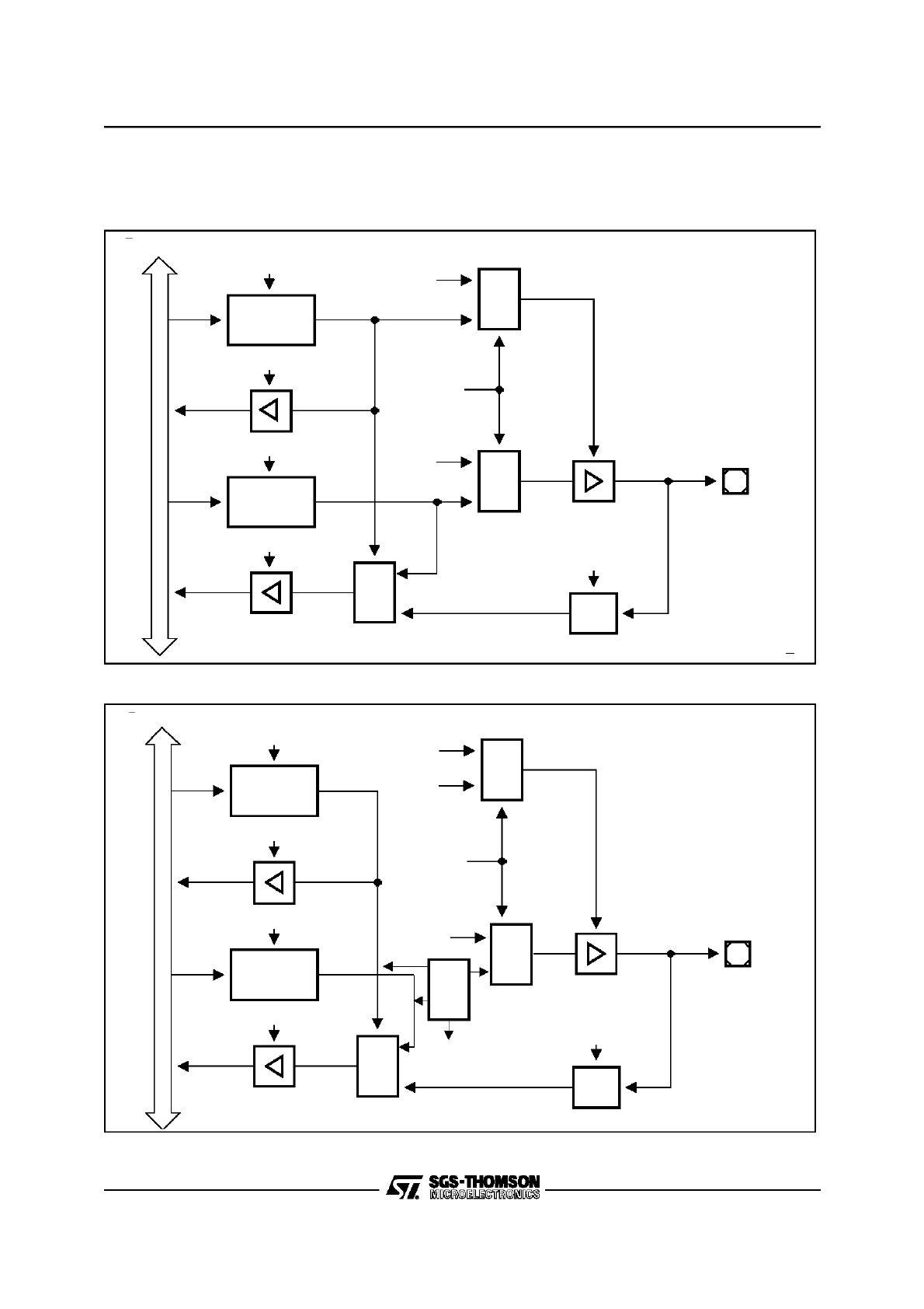
20/28
5 - PARALLEL PORTS (ST10R163)
PORT4 (Cont’d)
Figure 2-13. Block Diagram of Port 4 Pin P4.0 to P4.3
Figure 2-14. Block Diagram of Port 4 Pins SSPCE1/ A20, SSPCE0 / A21, SSPCLK / A2
VR02075B
Output
Buffer
MUX
1
0
Alternate
Data
Output
Latch
Port Output
0
1
MUX
Write P4.y
Read P4.y
Enable
Function
Alternate
0
1
MUX
Read DP4.y
Write DP4.y
Direction
’1’
Input
Latch
Clock
Latch
s
u
B
l
a
n
r
e
t
n
I
P4.y
y = 3...0
VR02075C
Output
Buffer
MUX
1
0
Alternate
Data
Output
Latch
Port Output
0
1
MUX
Write P4.y
Read P4.y
Enable
Function
Alternate
0
1
MUX
Read DP4.y
Write DP4.y
Direction
’1’
Input
Latch
Clock
Latch
s
u
B
l
a
n
r
e
t
n
I
P4.y
y = 4, 5, 7
Signal
Control
SSP
0
1
MUX
Signal
SSP
SSP
Enabled
96
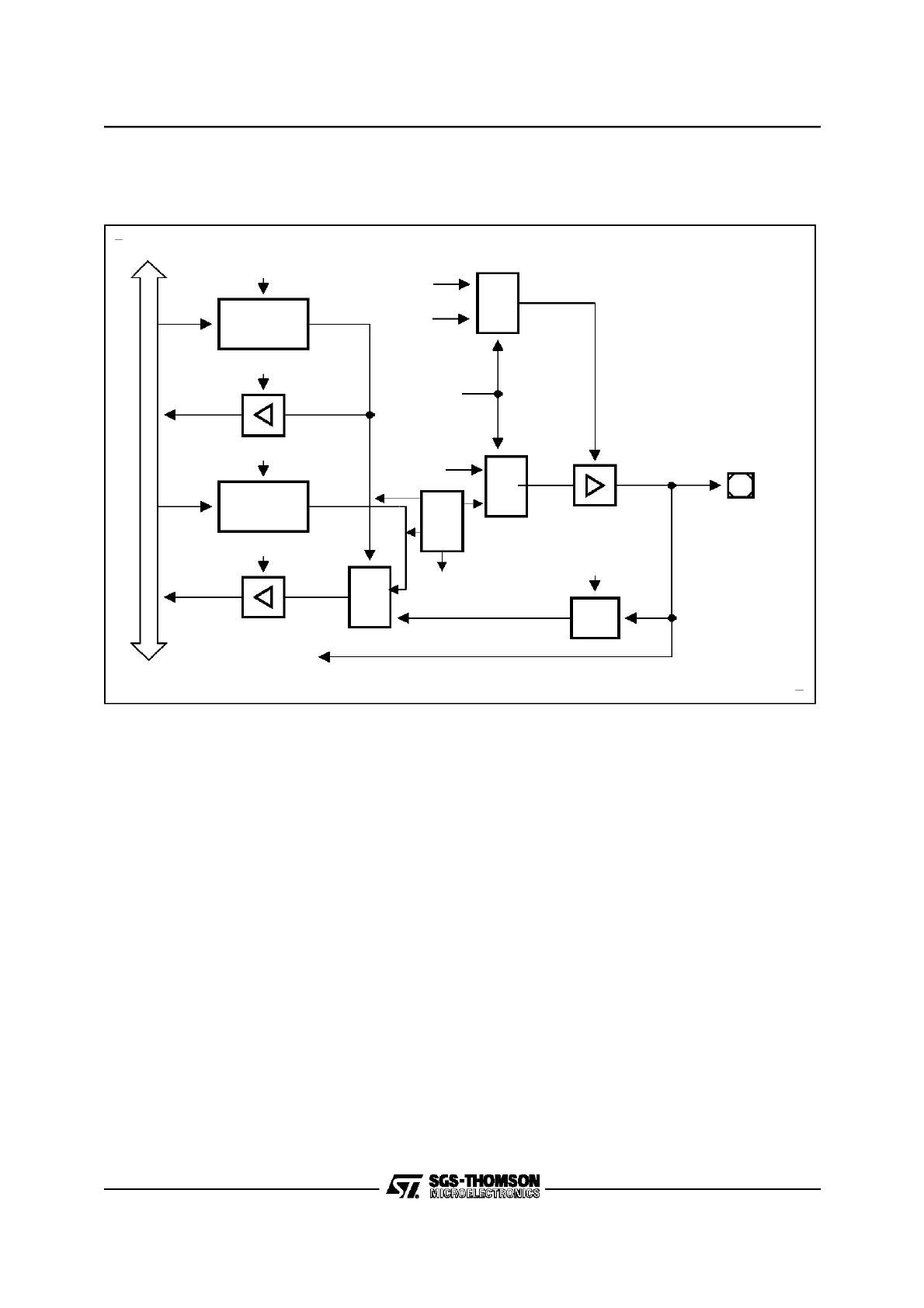
21/28
5 - PARALLEL PORTS (ST10R163)
PORT4 (Cont’d)
Figure 2-15. Block Diagram of Port 4 Pin SSPDAT/ A22
VR02075D
Output
Buffer
Latch
Port Output
0
1
MUX
Write P4.y
Read P4.y
Enable
Function
Alternate
0
1
MUX
Read DP4.y
Write DP4.y
Direction
’1’
Input
Latch
Clock
Latch
s
u
B
l
a
n
r
e
t
n
I
P4.6
Signal
Control
SSP
Data
Output
SSP
SSP
Data In
MUX
1
0
Alternate
Data
Output
0
1
MUX
SSP
Enabled
97
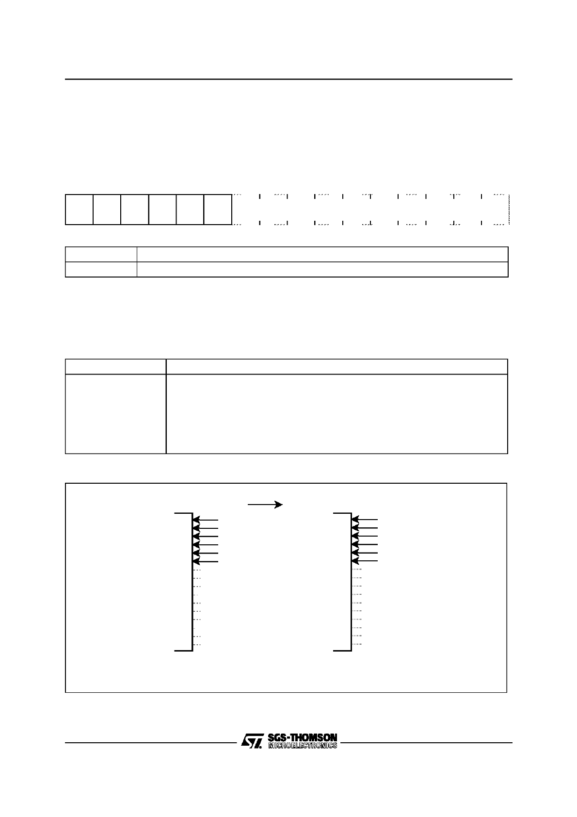
22/28
5 - PARALLEL PORTS (ST10R163)
5.5 PORT 5
This 6-bit input port can only read data. There is
no output latch and no direction register. Data writ-
ten to P5 will be lost.
P5 (FFA2h / D1h)
SFR
Reset Value: XX - -h
5.5.1 Alternate Functions of Port 5
Each line of Port 5 serves as external timer control
line for GPT1 and GPT2.
The table below summarizes the alternate func-
tions of Port 5.
Figure 2-16. Port 5 IO and Alternate Functions
Bit
Functio n
P5.y
Port data register P5 bit y (Read only)
5
4
3
2
1
0
11
10
9
8
7
6
15
14
13
12
-
-
-
-
-
-
r
r
-
-
-
-
r
r
r
r
P5.11
P5.12
P5.13
P5.14
P5.15
P5.10
Port 5 Pin
Alternate Function
P5.10
P5.11
P5.12
P5.13
P5.14
P5.15
T6EUD
Timer 6 external Up/Down Control Input
T5EUD
Timer 5 external Up/Down Control Input
T6IN
Timer 6 Count Input
T5IN
Timer 5 Count Input
T4EUD
Timer 4 external Up/Down Control Input
T2EUD
Timer 2 external Up/Down Control Input
P5.15
P5.14
P5.13
P5.12
P5.11
P5.10
-
-
-
-
-
-
-
-
-
-
Port 5
T2EUD
T4EUD
T5IN
T6IN
T5EUD
T6EUD
-
-
-
-
-
-
-
-
-
-
Alternate Function
a)
General Purpose
Input
98
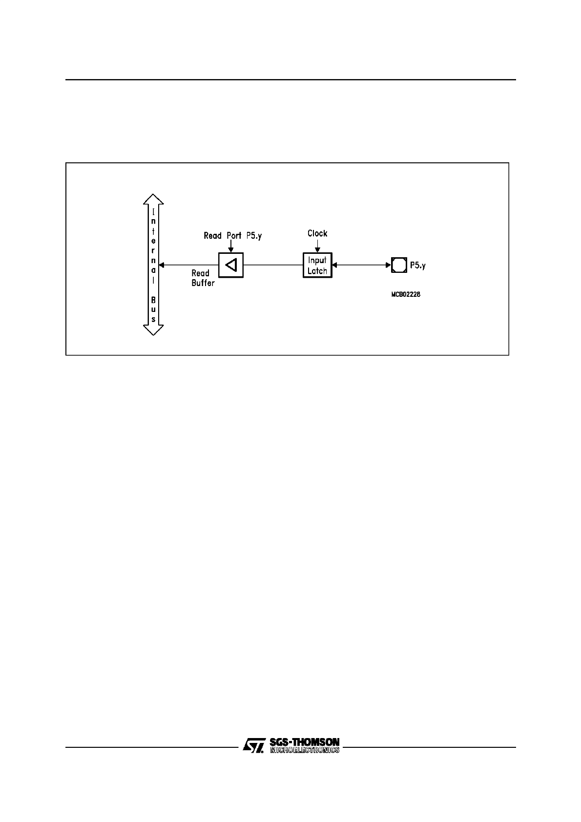
23/28
5 - PARALLEL PORTS (ST10R163)
PORT 5 (Cont’d)
Port 5 pins have a special port structure (see figure below), because it is an input only port.
Figure 2-17. Block Diagram of a Port 5 Pin
y = 15...10
99
24/28
5 - PARALLEL PORTS (ST10R163)
5.6 PORT 6
If this 8-bit port is used for general purpose IO, the
direction of each line can be configured via the
corresponding direction register DP6. Each port
line can be switched into push/pull or open drain
mode via the open drain control register ODP6.
P6 (FFCCh / E6h)
SFR
Reset Value: - - 00h
DP6 (FFCEh / E7h)
SFR
Reset Value: - - 00h
ODP6 (F1CEh / E7h)
ESFR
Reset Value: - - 00h
Bit
Function
P6.y
Port data register P6 bit y
Bit
Function
DP6.y
Port direction register DP6 bit y
DP6.y = 0: Port line P6.y is an input (high-impedance)
DP6.y = 1: Port line P6.y is an output
5
4
3
2
1
0
11
10
9
8
7
6
15
14
13
12
rw
rw
rw
rw
rw
rw
-
-
-
-
rw
rw
-
-
-
-
P6.0
P6.1
P6.2
P6.3
P6.4
P6.5
P6.6
P6.7
5
4
3
2
1
0
11
10
9
8
7
6
15
14
13
12
rw
rw
rw
rw
rw
rw
-
-
-
-
rw
rw
-
-
-
-
DP6.0
DP6.1
DP6.2
DP6.3
DP6.4
DP6.5
DP6.6
DP6.7
Bit
Function
ODP6.y
Port 6 Open Drain control register bit y
ODP6.y = 0: Port line P6.y output driver in push/pull mode
ODP6.y = 1: Port line P6.y output driver in open drain mode
5
4
3
2
1
0
11
10
9
8
7
6
15
14
13
12
rw
rw
rw
rw
rw
rw
-
-
-
-
rw
rw
-
-
-
-
ODP6
.7
ODP6
.6
ODP6
.5
ODP6
.4
ODP6
.3
ODP6
.2
ODP6
.1
ODP6
.0
100
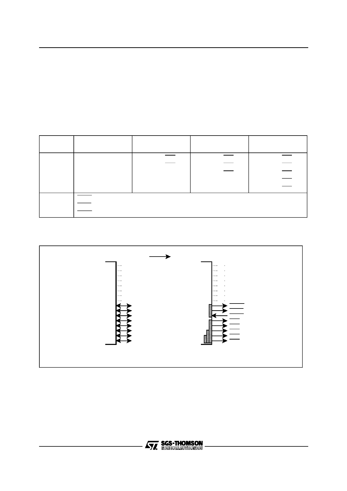
25/28
5 - PARALLEL PORTS (ST10R163)
PORT 6 (Cont’d)
5.6.1 Alternate Functions of Port 6
A programmable number of chip select signals
(CS4...CS0) derived from the bus control registers
(BUSCON4...BUSCON0) can be output on 5 pins
of Port 6. The other 3 pins may be used for bus ar-
bitration to accomodate additional masters in a
ST10R163 system.
The number of chip select signals is selected via
PORT0 during reset. The selected value can be
read from bitfield CSSEL in register RP0H (read
only) eg. in order to check the configuration during
run time.
The table below summarizes the alternate func-
tions of Port 6 depending on the number of select-
ed chip select lines (coded via bitfield CSSEL)
.
Figure 2-18. Port 6 IO and Alternate Functions
Port 6 Pin
Altern. Fun ction
CSSEL = 10
Altern. Function
CSSEL = 01
Altern. Functio n
CSSEL = 00
Altern. Function
CSSEL = 11
P6.0
P6.1
P6.2
P6.3
P6.4
Gen. purpose IO
Gen. purpose IO
Gen. purpose IO
Gen. purpose IO
Gen. purpose IO
Chip select CS0
Chip select CS1
Gen. purpose IO
Gen. purpose IO
Gen. purpose IO
Chip select CS0
Chip select CS1
Chip select CS2
Gen. purpose IO
Gen. purpose IO
Chip select CS0
Chip select CS1
Chip select CS2
Chip select CS3
Chip select CS4
P6.5
P6.6
P6.7
HOLDExternal hold request input
HLDAHold acknowledge output
BREQBus request output
-
-
-
-
-
-
-
-
P6.7
P6.6
P6.5
P6.4
P6.3
P6.2
P6.1
P6.0
Port 6
-
-
-
-
-
-
-
-
BREQ
HLDA
HOLD
CS4
CS3
CS2
CS1
CS0
Alternate Function
a)
General Purpose
Input/ Outpu t
101
26/28
5 - PARALLEL PORTS (ST10R163)
PORT 6 (Cont’d)
The chip select lines of Port 6 additionally have an
internal weak pullup device. This device is
switched on under the following conditions:
•
always during reset
•
if the Port 6 line is used as a chip select output,
and the ST10R163 is in Hold mode
(invoked through HOLD), and the respective pin
driver is in push/pull mode (ODP6.x = ‘0’).
This feature is implemented to drive the chip se-
lect lines high during reset in order to avoid multi-
ple chip selection, and to allow another master to
access the external memory via the same chip se-
lect lines (Wired-AND), while the ST10R163 is in
Hold mode.
With ODP6.x = ‘1’ (open drain output selected),
the internal pullup device will not be active during
Hold mode; external pullup devices must be used
in this case.
When entering Hold mode theCS lines are active-
ly driven high for one clock phase, then the output
level is controlled by the pullup devices (if activat-
ed).
After reset the CS function must be used, if select-
ed so. In this case there is no possibility to pro-
gram any port latches before. Thus the alternate
function (CS) is selected automatically in this
case.
Note: The open drain output option can only be
selected via software earliest during the ini-
tialization routine; at least signalCS0 will be
in push/pull output driver mode directly after
reset.
Figure 2-19. Block Diagram of Port 6 Pins with an alternate output function
102
27/28
5 - PARALLEL PORTS (ST10R163)
PORT 6 (Cont’d)
The bus arbitration signals HOLD, HLDA and
BREQ are selected with bit HLDEN in register
PSW. When the bus arbitration signals are ena-
bled via HLDEN, also these pins are switched au-
tomatically to the appropriate direction. Note that
the pin drivers for HLDA and BREQ are automati-
cally enabled, while the pin driver forHOLD is au-
tomatically disabled.
Figure 2-20. Block Diagram of Pin P6.5 (HOLD)
103

28/28
5 - PARALLEL PORTS (ST10R163)
Notes:
104

February 1996
1/2
This is advance information from SGS-TH OMSON. Details are subject tochange without notice.
ST10R163
User Manual
6 - DEDICATED PINS
Most of the input/output or control signals of the
functional the ST10R163 are realized as alternate
functions of pins of the parallel ports. There is,
however, a number of signals that use separate
pins, including the oscillator, special control sig-
nals and, of course, the power supply.
The table below summarizes the 23 dedicated
pins of the ST10R163.
The Address Latch Enable signal ALEcontrols
external address latches that provide a stable ad-
dress in multiplexed bus modes. ALE is activated /
not activated ...
The External Read Strobe RD controls the out-
put drivers of external memory or peripherals
when the ST10R163 reads data from these exter-
nal devices. During reset and during Hold mode
an internal pullup ensures an inactive (high) level
on the RD output.
The External Write Strobe WR/WRL controls the
data transfer from the ST10R163 to an external
memory or peripheral device. This pin may either
provide an general WR signal activated for both
byte and word write accesses, or specifically con-
trol the low byte of an external 16-bit device (WRL)
together with the signalWRH (alternate function of
P3.12/BHE). During reset and during Hold mode
an internal pullup ensures an inactive (high) level
on the WR/WRL output.
The Ready Input READY receives a control sig-
nal from an external memory or peripheral device
that is used to terminate an external bus cycle,
provided that this function is enabled for the cur-
rent bus cycle. READY may be used as synchro-
nous READY or may be evaluated asynchronous-
ly.
The External Access Enable Pin EA deter-
mines, if the ST10R163 after reset starts fetching
code from the internal ROM area (EA=’1’) or via
the external bus interface (EA=’0’).
The Non-Maskable Interrupt Input NMIallows to
trigger a high priority trap via an external signal
(eg. a power-fail signal). It also serves to validate
the
PWRDN
instruction
that
switches
the
ST10R163 into Power-Down mode.
The Reset Input RSTIN allows to put the
ST10R163 into the well defined reset condition ei-
ther at power-up or external events like a hard-
ware failure or manual reset. The input voltage
threshold of the RSTIN pin is raised compared to
the standard pins in order to minimize the noise
sensitivity of the reset input.
Pin(s)
Function
ALE
Address Latch Enable
RD
External Read Strobe
WR/WRL
External Write/Write Low Strobe
READY
Ready Input
EA
External Access Enable
NMI
Non-Maskable Interrupt Input
RSTIN
Reset Input
RSTOUT
Reset Output
XTAL1, XTAL2
Oscillator Input/Output
VPP
Reserved for Flash Programming
Voltage
VCC, VSS
Digital Power Supply and Ground
(6 pins each)
105

2/2
6 - DEDICATED PINS (ST10R163)
The Reset Output RSTOUT provides a special
reset signal for external circuitry.RSTOUT is acti-
vated at the beginning of the reset sequence, trig-
gered via RSTIN, a watchdog timer overflow or by
the SRST instruction. RSTOUT remains active
(low) until the EINIT instruction is executed. This
allows to initialize the controller before the exter-
nal circuitry is activated.
The Oscillator Input XTAL1 and Output XTAL2
connect the internal clock oscillator to the external
crystal. An external clock signal may be fed to the
input XTAL1, leaving XTAL2 open.
The Flash Programming Voltage input VPP
provides the programming voltage that is required
to erase and program the on-chip Flash memory
areas. On the ST10R163, the VPP pin is used to
Enable/Disable the Oscillator Watchdog (See
“System Clock Generation” section).
The Power Supply pins VCC and VSS provide
the power supply for the digital logic of the
ST10R163.
Note: All VCC pins and all VSS pins must be con-
nected to the power supply and ground, respec-
tively.
Figure 3-21
106
February 1996
1/24
This is advance information from SGS-TH OMSON. Details are subject tochange without notice.
ST10R163
User Manual
7 - EXTERNAL BUS INTERFACE
Although the ST10R163 provides a powerful set of
on-chip peripherals and on-chip RAM areas, these
internal units only cover a small fraction of its ad-
dress space of up to 16 MByte. The external bus
interface allows to access external peripherals
and additional volatile and non-volatile memory.
The external bus interface provides a number of
configurations, so it can be taylored to fit perfectly
into a given application system.
Accesses to external memory or peripherals are
executed by the integrated External Bus Control-
ler (EBC). The function of the EBC is controlled via
the SYSCON register and the BUSCONx and AD-
DRSELx registers. The BUSCONx registers spec-
ify the external bus cycles in terms of address
(mux/demux), data (16-bit/8-bit), chip selects and
length (waitstates / READY control / ALE / RW de-
lay). These parameters are used for accesses
within a specific address area which is defined via
the corresponding register ADDRSELx.
The four
pairs
BUSCON1/ADDRSEL1...BUS-
CON4/ADDRSEL4 allow to define four independ-
ent “address windows”, while all external accesses
outside these windows are controlled via register
BUSCON0.
Figure 4-1. SFRs and Port Pins Associated with the External Bus Interface
BUSCON0
BUSCON1
BUSCON2
ADDRSEL4
P0L / P0H
P4
P6
ADDRSEL1
ODP6
E
P0L/P0H
PORT0 Data Registers
P1L/P1H
PORT1 Data Registers
DP3
Port 3 Direction Control Register
P3
Port 3 Data Register
P4
Port 4 Data Register
ODP6
Port 6 Open Drain Control Register
DP6
Port 6 Direction Control Register
P6
Port 6 Data Register
PORT0
EA
PORT1
RSTIN
ALE
READY
RD
WR/WRL
BHE/WRH
SYSCON
Control Registers
ADDRSELx Address Range Select Register 1...4
BUSCO Nx
Bus Mode Control Register 0...4
SYSC ON
System Control Register
RP0H
Port P0H Reset Configuration Register
Ports & Direction Control
Alternate Functions
Address Registers
Mode Registers
Control Registers
BUSCON3
P1L / P1H
BUSCON4
ADDRSEL2
RP0H
DP6
DP3
P3
ADDRSEL3
107

2/24
7 - EXTERNAL BUS INTERFACE (ST10R163)
7.1 SINGLE CHIP MODE
Single chip mode is entered, when pinEA is high
during reset. In this case register BUSCON0 is
cleared (except bit ALECTL0 and bits BTYP0[1:0]
= P0L.[7:6]), which also resets bit BUSACT0 of
BUSCON0 register, so no external bus is enabled.
In single chip mode the ST10R163 operates only
with and out of internal resources. No external bus
is configured and no external peripherals and/or
memory can be accessed. Also no port lines are
occupied for the bus interface. The ST10R165 be-
ing a Romless device, it cannot operate in single
chip mode. Hence, the EA pin must be forced at 0
during reset.
7.2 EXTERNAL BUS MODES
When the external bus interface is enabled (bit
BUSACTx=’1’) and configured (bitfield BTYP), the
ST10R163 uses a subset of its port lines together
with some control lines to build the external bus.
The bus configuration (BTYP) for the address win-
dows (BUSCON4...BUSCON1) is selected via
software typically during the initialization of the
system.
The bus configuration (BTYP) for the default ad-
dress range (BUSCON0) is selected via PORT0
during reset, provided that pinEA is low during re-
set. Afterwards, BUSCON0 may be modified via
software just like the other BUSCON registers.
The 16 MByte address space of the ST10R163 is
divided into 256 segments of 64 KByte each. The
16-bit intra-segment address is output on PORT0
for multiplexed bus modes or on PORT1 for de-
multiplexed bus modes. When segmentation is
disabled, only one 64 KByte segment can be used
and accessed. Otherwise additional address lines
may be output on Port 4, and/or several chip se-
lect lines may be used to select different memory
banks or peripherals. These functions are select-
ed during reset via bitfields SALSEL and CSSEL
of register RP0H, respectively.
Note: Bit SGTDIS of register SYSCON defines, if
the CSP register is saved during interrupt entry
(segmentation active) or not (segmentation disa-
bled).
Multiplexed Bus Modes
In the multiplexed bus modes the 16-bit intra-seg-
ment address as well as the data use PORT0. The
address is time-multiplexed with the data and has
to be latched externally. The width of the required
latch depends on the selected data bus width, ie.
an 8-bit data bus requires a byte latch (the ad-
dress bits A15...A8 on P0H do not change, while
P0L multiplexes address and data), a 16-bit data
bus requires a word latch (the least significant ad-
dress line A0 is not relevant for word accesses).
The upper address lines (An...A16) are perma-
nently output on Port 4 (if segmentation is ena-
bled) and do not require latches.
The EBC initiates an external access by generat-
ing the Address Latch Enable signal (ALE) and
then placing an address on the bus. The falling
edge of ALE triggers an external latch to capture
the address. After a period of time during which
the address must have been latched externally,
the address is removed from the bus. The EBC
now activates the respective command signal
(RD, WR, WRL, WRH). Data is driven onto the
bus either by the EBC (for write cycles) or by the
external memory/peripheral (for read cycles). Af-
ter a period of time, which is determined by the ac-
cess time of the memory/peripheral, data become
valid.
Read cycles: Input data is latched and the com-
mand signal is now deactivated. This causes the
accessed device to remove its data from the bus
which is then tri-stated again.
Write cycles: The command signal is now deacti-
vated. The data remain valid on the bus until the
next external bus cycle is started.
BTYP Encoding
External Data Bus Width
External Address Bus Mode
0 0
8-bit Data
Demultiplexed Addresses
0 1
8-bit Data
Multiplexed Addresses
1 0
16-bit Data
Demultiplexed Addresses
1 1
16-bit Data
Multiplexed Addresses
108
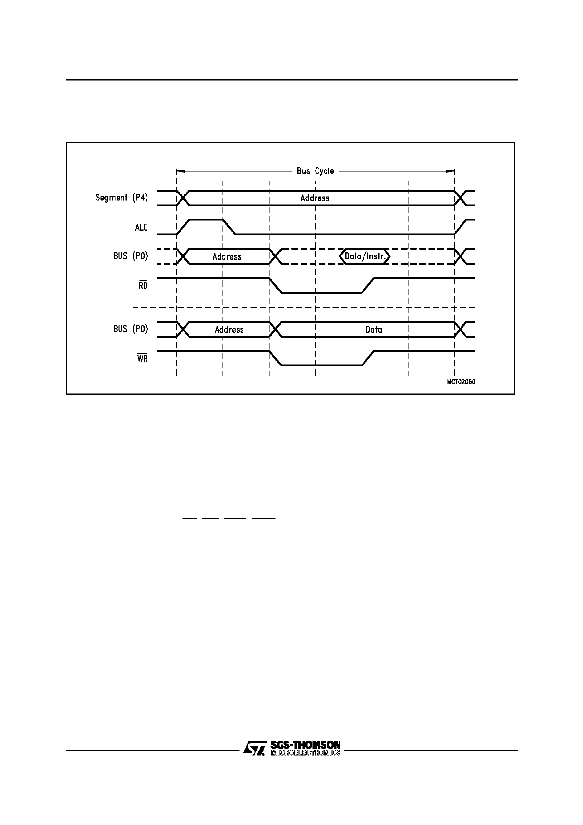
3/24
7 - EXTERNAL BUS INTERFACE (ST10R163)
EXTERNAL BUS MODES (Cont’d)
Figure 4-2. Multiplexed Bus Cycle
Demultiplexed Bus Modes
In the demultiplexed bus modes the 16-bit intra-
segment
address
is permanently
output
on
PORT1, while the data uses PORT0 (16-bit data)
or P0L (8-bit data).
The upper address lines are permanently output
on Port 4 (if selected via SALSEL during reset).
No address latches are required.
The EBC initiates an external access by placing
an address on the address bus. After a program-
mable period of time the EBC activates the re-
spective command signal (RD, WR, WRL, WRH).
Data is driven onto the data bus either by the EBC
(for write cycles) or by the external memory/pe-
ripheral (for read cycles). After a period of time,
which is determined by the access time of the
memory/peripheral, data become valid.
Read cycles: Input data is latched and the com-
mand signal is now deactivated. This causes the
accessed device to remove its data from the data
bus which is then tri-stated again.
Write cycles: The command signal is now deacti-
vated. If a subsequent external bus cycle is re-
quired, the EBC places the respective address on
the address bus. The data remain valid on the bus
until the next external bus cycle is started.
109
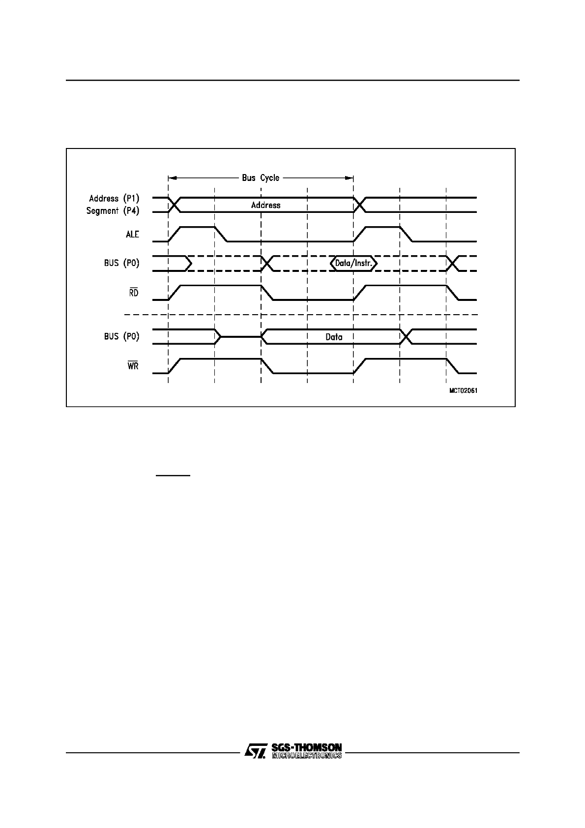
4/24
7 - EXTERNAL BUS INTERFACE (ST10R163)
EXTERNAL BUS MODES (Cont’d)
Figure 4-3. Demultiplexed Bus Cycle
Switching between the Bus Modes
The EBC allows to switch between different bus
modes dynamically, ie. subsequent external bus
cycles may be executed in different ways. Certain
address areas may use multiplexed or demulti-
plexed buses or use READY control or predefined
waitstates.
A change of the external bus characteristics can
be initiated in two different ways:
Reprogramming the BUSCON and/or ADDR-
SEL registers allows to either change the bus
mode for a given address window, or change the
size of an address window that uses a certain bus
mode. Reprogramming allows to use a great
number of different address windows (more than
BUSCONs are available) on the expense of the
overhead for changing the registers and keeping
appropriate tables.
Switching between predefined address win-
dows automatically selects the bus mode that is
associated with the respective window. Prede-
fined address windows allow to use different bus
modes without any overhead, but restrict their
number to the number of BUSCONs. However, as
BUSCON0 controls all address areas, which are
not covered by the other BUSCONs, this allows to
have gaps between these windows, which use the
bus mode of BUSCON0.
PORT1 will output the intra-segment address,
when any of the BUSCON registers selects a de-
multiplexed bus mode, even if the current bus cy-
cle uses a multiplexed bus mode. This allows to
have an external address decoder connected to
PORT1 only, while using it for all kinds of bus cy-
cles.
Note: Never change the configuration for an ad-
dress area that currently supplies the instruction
stream. Due to the internal pipelining it is very dif-
ficult to determine the first instruction fetch that will
use the new configuration. Only change the con-
figuration for address areas that are not currently
accessed. This applies to BUSCON registers as
well as to ADDRSEL registers.
The usage of the BUSCON/ADDRSEL registers is
controlled via the issued addresses. When an ac-
cess (code fetch or data) is initiated, the respec-
tive generated physical address defines, if the ac-
cess is made internally, uses one of the address
windows defined by ADDRSEL4...1, or uses the
default configuration in BUSCON0. After initializ-
ing the active registers, they are selected and
evaluated automatically by interpreting the physi-
cal address. No additional switching or selecting is
necessary during run time, except when more
than the four address windows plus the default is
to be used.
110
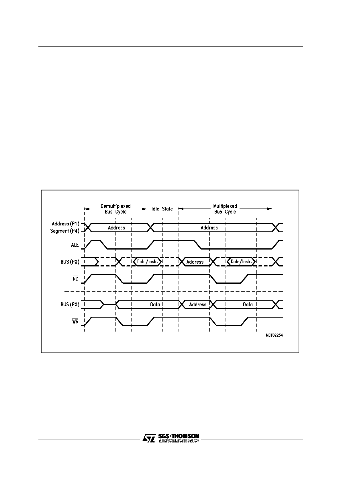
5/24
7 - EXTERNAL BUS INTERFACE (ST10R163)
EXTERNAL BUS MODES (Cont’d)
Switching from demultiplexed to multiplexed
bus mode represents a special case. The bus cy-
cle is started by activating ALE and driving the ad-
dress to Port 4 and PORT1 as usual, if another
BUSCON register selects a demultiplexed bus.
However, in the multiplexed bus modes the ad-
dress is also required on PORT0. In this special
case the address on PORT0 is delayed by one
CPU clock cycle, which delays the complete (mul-
tiplexed) bus cycle and extends the corresponding
ALE signal (see figure below).
This extra time is required to allow the previously
selected device (via demultiplexed bus) to release
the data bus, which would be available in a demul-
tiplexed bus cycle.
External Data Bus Width
The EBC can operate on 8-bit or 16-bit wide exter-
nal memory/peripherals. A 16-bit data bus uses
PORT0, while an 8-bit data bus only uses P0L, the
lower byte of PORT0. This saves on address
latches, bus transceivers, bus routing and memo-
ry cost on the expense of transfer time. The EBC
can control word accesses on an 8-bit data bus as
well as byte accesses on a 16-bit data bus.
Word accesses on an 8-bit data busare auto-
matically split into two subsequent byte accesses,
where the low byte is accessed first, then the high
byte. The assembly of bytes to words and the dis-
assembly of words into bytes is handled by the
EBC and is transparent to the CPU and the pro-
grammer.
Figure 4-4. Switching from demultiplexed to Multiplexed Bus Mode
111
6/24
7 - EXTERNAL BUS INTERFACE (ST10R163)
EXTERNAL BUS MODES (Cont’d)
Byte accesses on a 16-bit data bus require that
the upper and lower half of the memory can be ac-
cessed individually. In this case the upper byte is
selected with the BHE signal, while the lower byte
is selected with the A0 signal. So the two bytes of
the memory can be enabled independent from
each other, or together when accessing words.
When writing bytes to an external 16-bit device,
which has a single CS input, but two WR enable
inputs (for the two bytes), the EBC can directly
generate these two write control signals. This
saves the external combination of theWR signal
with A0 or BHE. In this case pin WR serves as
WRL (write low byte) and pin BHE serves as WRH
(write high byte). Bit WRCFG in register SYSCON
selects the operating mode for pinsWR and BHE.
The respective byte will be written on both data
bus halves.
When reading bytes from an external 16-bit de-
vice, whole words may be read and the ST10R163
automatically selects the byte to be input and dis-
cards the other. However, care must be taken
when reading devices that change state when be-
ing read, like FIFOs, interrupt status registers, etc.
In this case individual bytes should be selected
using BHE and A0.
PORT1 gets available for general purpose IO,
when none of the BUSCON registers selects a de-
multiplexed bus mode.
Disable/Enable Control for PinBHE (BYTDIS)
Bit BYTDIS of SYSCON register is provided for
controlling the active low Byte High Enable (BHE)
pin. The function of the BHE pin is enabled, if the
BYTDIS bit contains a ’0’. Otherwise, it is disabled
and the pin can be used as standard IO pin. The
BHE pin is implicitly used by the External Bus
Controller to select one of two byte-organized
memory chips, which are connected to the
ST10R163 via a word-wide external data bus. Af-
ter reset the BHE function is automatically ena-
bled (BYTDIS = ’0’), if a 16-bit data bus is selected
during reset, otherwise it is disabled (BYTDIS=’1’).
It may be disabled, if byte access to 16-bit memo-
ry is not required, and the BHE signal is not used.
Segment Address Generation
During external accesses the EBC generates a
(programmable) number of address lines on Port
4, which extend the 16-bit address output on
PORT0 or PORT1, and so increase the accessible
address space. The number of segment address
lines is selected during reset and coded in bit field
SALSEL in register RP0H (see table below).
Note: The total accessible address space may be
increased by accessing several banks which are
distinguished by individual chip select signals.
Bus Mode
Transfer Rate (Speed factor for
byte/word/dword access)
System Requirements
Free IO Lines
8-bit Multiplexed
Very low
( 1.5 / 3 / 6 )
Low (8-bit latch, byte bus)
P1H, P1L
8-bit Demultipl.
Low
( 1 / 2 / 4 )
Very low (no latch, byte bus)
P0H
16-bit Multiplexed
High
( 1.5 / 1.5 / 3 )
High (16-bit latch, word bus)
P1H, P1L
16-bit Demultipl.
Very high
( 1 / 1 / 2 )
Low (no latch, word bus)
---
SALSEL
Segment Address Lines
Directly accessible Address Space
1 1
Two:A17...A16
256KByte (Default without pull-downs)
1 0
Eight:A23...A16
16MByte (Maximum)
0 1
None
64KByte (Minimum)
0 0
Four:A19...A16
1MByte
112
7/24
7 - EXTERNAL BUS INTERFACE (ST10R163)
EXTERNAL BUS MODES (Cont’d)
CS Signal Generation
During external accesses the EBC can generate a
(programmable) number of CS lines on Port 6,
which allow to directly select external peripherals
or memory banks without requiring an external de-
coder. The number of CS lines is selected during
reset and coded in bit field CSSEL in register
RP0H
(see
table
below).
The CSx outputs are associated with the BUS-
CONx registers and are driven active (low) for any
access within the address area defined for the re-
spective BUSCON register. For any access out-
side this defined address area the respectiveCSx
signal will go inactive (high).
Note: No CSx signal will be generated for an ac-
cess to any internal address area, even if this area
is covered by the respective ADDRSELx register.
The chip select signals allow to be operated in four
different modes, which are selected via bits CS-
WENx and CSRENx in the respective BUSCONx
register.
Address Chip Select signals remain active for
the whole external bus cycle. An address chip se-
lect becomes active with the falling edge of ALE
and becomes inactive with the falling edge of ALE
of an external bus cycle that accesses a different
address area. No spikes will be generated on the
chip select lines.
Read or Write Chip Select signals remain active
only as long as the associated control signal (RD
or WR) is active. This also includes the program-
mable read/write delay. Read chip select is only
activated for read cycles, write chip select is only
activated for write cycles, read/write chip select is
activated for both read and write cycles (write cy-
cles are assumed, if any of the signals WRH or
WRL gets active). These modes save external
glue logic, when accessing external devices like
latches or drivers that only provide a single enable
input.
CS0 provides an address chip select directly after
reset (except for single chip mode) when the first
instruction is fetched.
Internal pullup devices hold the selectedCS lines
high during reset. After the end of a reset se-
quence the pullup devices are switched off and
the pin drivers control the pin levels on the select-
ed CS lines. Not selected CS lines will enter the
high-impedance state and are available for gener-
al purpose IO.
The pullup devices are also active during bus
hold, while HLDA is active and the respective pin
is switched to push/pull mode. Open drain outputs
will float during bus hold. In this case external pul-
lup devices are required or the new bus master is
responsible for driving appropriate levels on the
CS lines.
Segment Address versus Chip Select
The external bus interface of the ST10R163 sup-
ports many configurations for the external memo-
ry. By increasing the number of segment address
lines the ST10R163 can address a linear address
space of 256 KByte, 1 MByte or 16 MByte. This al-
lows to implement a large sequential memory ar-
ea, and also allows to access a great number of
external devices, using an external decoder. By
increasing the number of CS lines the ST10R163
can access memory banks or peripherals without
external glue logic. These two features may be
combined to optimize the overall system perform-
ance. Enabling 4 segment address lines and 5
chip select lines eg. allows to access five memory
banks of 1 MByte each. So the available address
space is 5 MByte (without glue logic).
Note: Bit SGTDIS of register SYSCON defines, if
the CSP register is saved during interrupt entry
(segmentation active) or not (segmentation disa-
bled).
CSSEL Chip Select Lines Note
1 1
Five:CS4...CS0
Default without pull-downs
1 0
None
Port 6 pins free for IO
0 1
Two:CS1...CS0
0 0
Three:CS2...CS0
CSWENx
CSRENx
Chip Select Mode
0
0
Address Chip Select (Default
after Reset)
0
1
Read Chip Select
1
0
Write Chip Select
1
1
Read/Write Chip Select
113
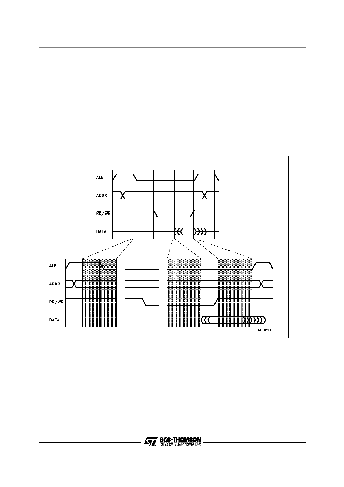
8/24
7 - EXTERNAL BUS INTERFACE (ST10R163)
7.3 PROGRAMMABLE BUS CHARACTERISTICS
Important timing characteristics of the external
bus interface have been made user programma-
ble to allow to adapt it to a wide range of different
external bus and memory configurations with dif-
ferent types of memories and/or peripherals.
The following parameters of an external bus cycle
are programmable:
•
ALE Control defines the ALE signal length and
the address hold time after its falling edge
•
Memory Cycle Time (extendable with 1...15
waitstates) defines the allowable access time
•
Memory Tri-State Time(extendable with 1 wait-
state) defines the time for a data driver to float
•
Read/Write Delay Time defines when a com-
mand is activated after the falling edge of ALE
•
READY Control defines, if a bus cycle is termi-
nated internally or externally
Note: Internal accesses are executed with maxi-
mum speed and therefore are not programmable.
External acceses use the slowest possible bus cy-
cle after reset. The bus cycle timing may then be
optimized by the initialization software.
Figure 4-5. Programmable External Bus Cycle
ALECTL
MCTC
MTTC
114
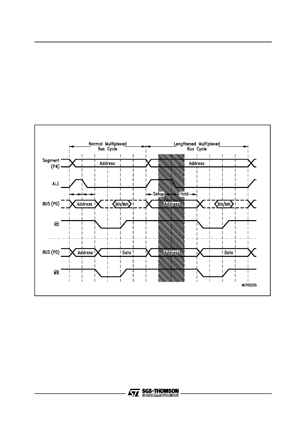
9/24
7 - EXTERNAL BUS INTERFACE (ST10R163)
PROGRAMMABLE BUS CHARACTERISTICS(Cont’d)
ALE Length Control
The length of the ALE signal and the address hold
time after its falling edge are controlled by the
ALECTLx bits in the BUSCON registers. When bit
ALECTL is set to ‘1’, external bus cycles access-
ing the respective address window will have their
ALE signal prolonged by half a CPU clock (25 ns
at
fCPU = 20 MHz). Also the address hold time af-
ter the falling edge of ALE (on a multiplexed bus)
will be prolonged by half a CPU clock, so the data
transfer within a bus cycle refers to the same CLK-
OUT edges as usual (ie. the data transfer is de-
layed by one CPU clock). This allows more time
for the address to be latched.
Note: ALECTL0 is ‘1’ after reset to select the slow-
est possible bus cycle, the other ALECTLx are ‘0’
after reset.
Figure 4-6. ALE Length Control
115
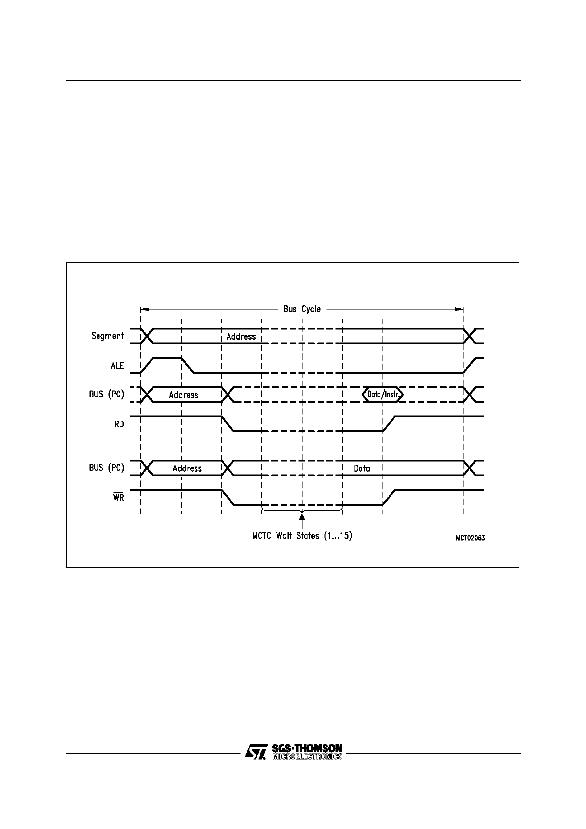
10/24
7 - EXTERNAL BUS INTERFACE (ST10R163)
PROGRAMMABLE BUS CHARACTERISTICS(Cont’d)
Programmable Memory Cycle Time
The ST10R163 allows the user to adjust the con-
troller’s external bus cycles to the access time of
the respective memory or peripheral. This access
time is the total time required to move the data to
the destination. It represents the period of time
during which the controller’s signals do not
change.
The external bus cycles of the ST10R163 can be
extended for a memory or peripheral, which can-
not keep pace with the controller’s maximum
speed, by introducing wait states during the ac-
cess (see figure above). During these memory cy-
cle time wait states, the CPU is idle, if this access
is required for the execution of the current instruc-
tion.
The memory cycle time wait states can be pro-
grammed in increments of one CPU clock (50 ns
at
fCPU = 20 MHz) within a range from 0 to 15 (de-
fault after reset) via the MCTC fields of the BUS-
CON registers. 15-<MCTC> waitstates will be in-
serted.
Figure 4-7. Memory Cycle Time
116
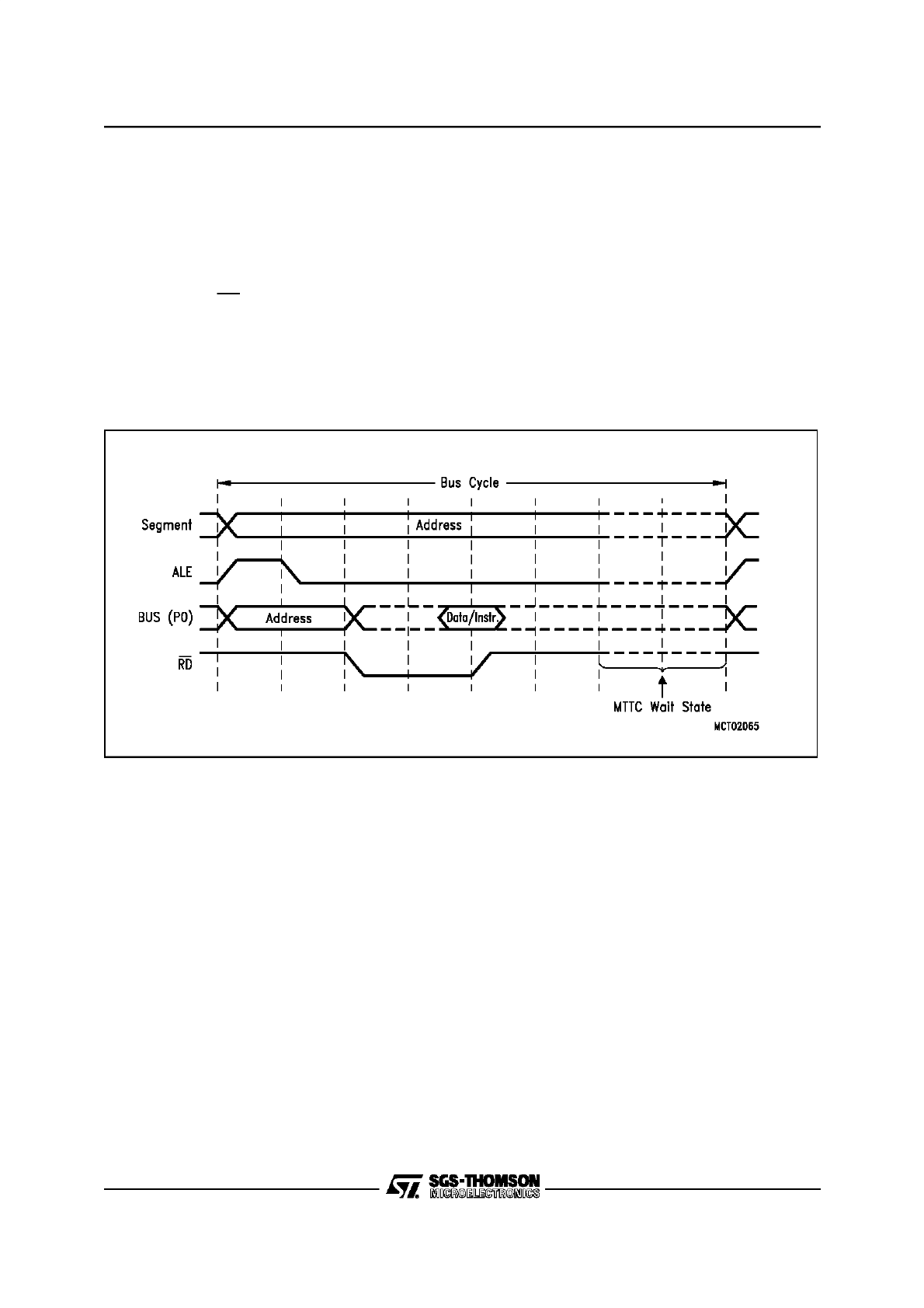
11/24
7 - EXTERNAL BUS INTERFACE (ST10R163)
PROGRAMMABLE BUS CHARACTERISTICS(Cont’d)
Programmable Memory Tri-State Time
The ST10R163 allows the user to adjust the time
between two subsequent external accesses to ac-
count for the tri-state time of the external device.
The tri-state time defines, when the external device
has released the bus after deactivation of the
read command (RD).
The output of the next address on the external bus
can be delayed for a memory or peripheral, which
needs more time to switch off its bus drivers, by in-
troducing a waitstate after the previous bus cycle
(see figure above). During this memory tri-state
time wait state, the CPU is not idle, so CPU oper-
ations will only be slowed down if a subsequent
external instruction or data fetch operation is re-
quired during the next instruction cycle.
The memory tri-state time waitstate requires one
CPU clock (50 ns at
fCPU = 20 MHz) and is con-
trolled via the MTTCx bits of the BUSCON regis-
ters. A waitstate will be inserted, if bit MTTCx is ‘0’
(default after reset).
Note: External bus cycles in multiplexed bus
modes implicitly add one tri-state time waitstate in
addition to the programmable MTTC waitstate.
Figure 4-8. Memory Tri-State Time
117
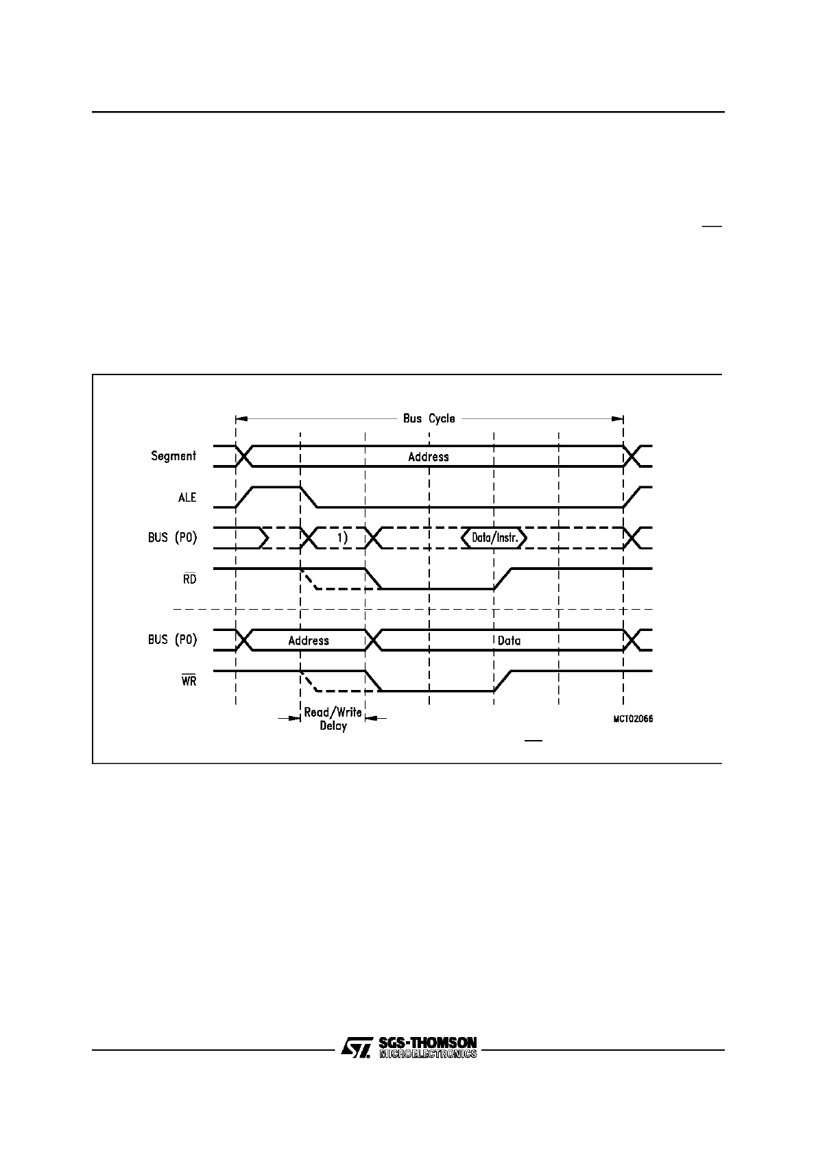
12/24
7 - EXTERNAL BUS INTERFACE (ST10R163)
PROGRAMMABLE BUS CHARACTERISTICS(Cont’d)
Read/Write Signal Delay
The ST10R163 allows the user to adjust the timing
of the read and write commands to account for
timing requirements of external peripherals. The
read/write delay controls the time between the fall-
ing edge of ALE and the falling edge of the com-
mand. Without read/write delay the falling edges
of ALE and command(s) are coincident (except for
propagation delays). With the delay enabled, the
command(s) become active half a CPU clock (25
ns at
fCPU = 20 MHz) after the falling edge of
ALE.
The read/write delay does not extend the memory
cycle time, and does not slow down the controller
in general. In multiplexed bus modes, however,
the data drivers of an external device may conflict
with the ST10R163’s address, when the earlyRD
signal is used. Therefore multiplexed bus cycles
should always be programmed with read/write de-
lay.
The read/write delay is controlled via the RWDCx
bits in the BUSCON registers. The command(s)
will be delayed, if bit RWDCx is ‘0’ (default after re-
set).
Figure 4-9. Read/Write Delay
1) The data drivers from the previous bus cycle should be disabled when the RD signal becomes active.
118
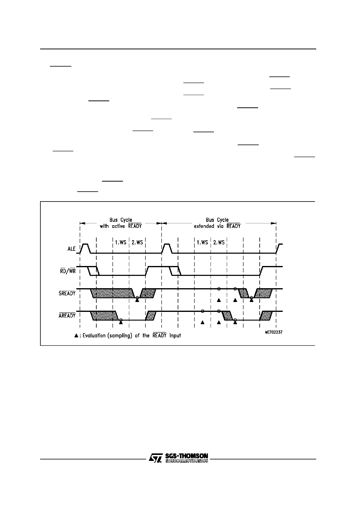
13/24
7 - EXTERNAL BUS INTERFACE (ST10R163)
7.4 READY CONTROLLED BUS CYCLES
For situations, where the programmable wait-
states are not enough, or where the response (ac-
cess) time of a peripheral is not constant, the
ST10R163 provides external bus cycles that are
terminated via a READY input signal (synchro-
nous
or
asynchronous).
In
this
case
the
ST10R163 first inserts a programmable number of
waitstates (0...7) and then monitors the READY
line to determine the actual end of the current bus
cycle. The external device drives READY low in
order to indicate that data have been latched
(write cycle) or are available (read cycle).
The READY function is enabled via the RDYENx
bits in the BUSCON registers. When this function
is selected (RDYENx = ‘1’), only the lower 3 bits of
the respective MCTC bit field define the number of
inserted waitstates (0...7), while the MSB of bit
field MCTC selects the READY operation:
MCTC.3 = ‘0’: Synchronous READY, ie. the
READY signal must meet setup and hold times.
MCTC.3 = ‘1’: Asynchronous READY, ie. the
READY signal is synchronized internally.
The synchronous READY provides the fastest
bus cycles, but requires setup and hold times to
be met. The CLKOUT signal must be enabled
and may be used by the peripheral logic to control
the READY timing in this case.
The asynchronous READY is less restrictive, but
requires additional waitstates caused by the inter-
nal synchronization. As the asynchronousREADY
is sampled earlier (see figure above) programmed
waitstates may be necessary to provide proper
bus cycles (see also notes on “normally-ready”
peripherals below).
Figure 4-10. READY Controlled Bus Cycles
119

14/24
7 - EXTERNAL BUS INTERFACE (ST10R163)
READY CONTROLLED BUS CYCLES (Cont’d)
A
READY
signal
(especially
asynchronous
READY) that has been activated by an external
device may be deactivated in response to the trail-
ing (rising) edge of the respective command (RD
or WR).
Note: When the READY function is enabled for a
specific address window, each bus cycle within
this window must be terminated with an active
READY signal. Otherwise the controller hangs un-
til the next reset. A timeout function is only provid-
ed by the watchdog timer.
Combining the READY function with prede-
fined waitstates is advantageous in two cases:
Memory components with a fixed access time and
peripherals
operating
with READY may
be
grouped into the same address window. The (ex-
ternal) waitstate control logic in this case would
activate READY either upon the memory’s chip
select or with the peripheral’s READY output. Af-
ter the predefined number of waitstates the
ST10R163 will check its READY line to determine
the end of the bus cycle. For a memory access it
will be low already (see example a) in the figure
above), for a peripheral access it may be delayed
(see example b) in the figure above). As memories
tend to be faster than peripherals, there should be
no impact on system performance.
When using the READY function with “normally-
ready” peripherals, it may lead to erroneous bus
cycles, if the READY line is sampled too early.
These peripherals pull their READY output low,
while they are idle. When they are accessed, they
deactivate READY until the bus cycle is complete,
then drive it low again. If, however, the peripheral
deactivates READY after the first sample point of
the ST10R163, the controller samples an active
READY and terminates the current bus cycle,
which, of course, is too early. By inserting prede-
fined waitstates the firstREADY sample point can
be shifted to a time, where the peripheral has
safely controlled the READY line (eg. after 2 wait-
states in the figure above).
7.5
CONTROLLING
THE
EXTERNAL
BUS
CONTROLLER
A set of registers controls the functions of the
EBC. General features like the usage of interface
pins (WR, BHE), segmentation and internal ROM
mapping are controlled via register SYSCON. The
properties of a bus cycle like chip select mode, us-
age of READY, length of ALE, external bus mode,
read/write delay and waitstates are controlled via
registers BUSCON4...BUSCON0. Four of these
registers (BUSCON4...BUSCON1) have an ad-
dress select register (ADDRSEL4...ADDRSEL1)
associated with them, which allows to specify up
to four address areas and the individual bus char-
acteristics within these areas. All accesses that
are not covered by these four areas are then con-
trolled via BUSCON0. This allows to use memory
components or peripherals with different interfac-
es within the same system, while optimizing ac-
cesses to each of them.
120
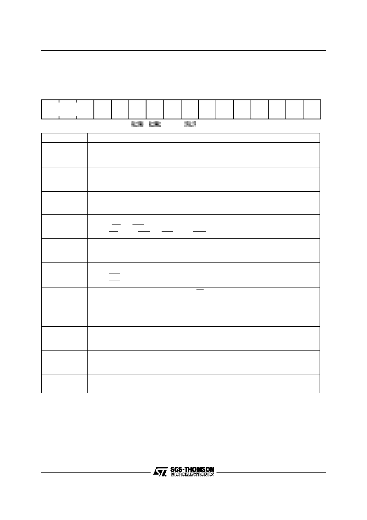
15/24
7 - EXTERNAL BUS INTERFACE (ST10R163)
CONTROLLING THE EXTERNAL BUS CONTROLLER(Cont’d)
SYSCON (FF12h / 89h)
SFR
Reset Value: 0XX0h
Note: Register SYSCON cannot be changed after execution of the EINIT instruction.
Bit SGTDIS controls the correct stack operation (push/pop of CSP or not) during traps and interrupts. Bits marked
with “-” must be kept at 0.
Bit
Function
XPER-SHARE
XBUS Peripheral Share Mode Control
‘0’: External accesses to XBUS peripherals are disbled
‘1’: XBUS peripherals are accessible via the external bus during hold mode.
VISIBLE
Visible Mode Control
‘0’: Accesses to XBUS peripherals are done internally
‘1’: XBUS peripheral accesses are made visible on the external pins.
SSPEN
Xperipheral SSP Enable Control
‘0’: SSP is disabled. Pins P4.[7..4] are general purpose IOs or segment address lines
‘1’: SSP is enabled. Pins P4.[7..4] are SSP IOs or segment address lines
WRCFG
Write Configur ation Control (Set according to pin P0H.0 during reset)
‘0’: Pins WR and BHE retain their normal function
‘1’: Pin WR acts as WRL, pin BHE acts as WRH
CLKEN
System Clock Outp ut Enable (CLKOUT)
‘0’: CLKOUT disabled: pin may be used for general purpose IO
‘1’: CLKOUT enabled: pin outputs the system clock signal
BYTDIS
Disable/Enabl e Control for Pin BHE (Set according to data bus width)
‘0’: Pin BHE enabled
‘1’: Pin BHE disabled, pin may be used for general purpose IO
ROMEN
Internal ROM Enable (Set according to pin EA during reset)
‘0’: Internal ROM disabled: accesses to the ROM area use the external bus
‘1’: Internal ROM enabled
This bit is not relevant on the ST10R165, since it does not include internal ROM. It should be
kept at 0
SGTDIS
Segmentation Disable/Enable Control
‘0’: Segmentation enabled (CSP is saved/restored during interrupt entry/exit)
‘1’: Segmentation disabled (Only IP is saved/restored)
ROMS1
Internal ROM mapping
This bit is not relevant on the ST10R165, since it does not include internal ROM. It should be
kept at 0.
STKSZ
System Stack Size
Selects the size of the system stack (in the internal RAM) from 32 to 1024 words
XPER-
SHARE
VISI
BLE
-
-
-
-
SSP
EN
ROM
S1
WR
CFG
5
4
3
2
1
0
11
10
9
8
7
6
15
14
13
12
-
-
rw
rw
rw
rw
rw
rw
STKSZ
SGT
DIS
ROM
EN
-
BYT
DIS
CLK
EN
rw
-
rw
rw
-
121
16/24
7 - EXTERNAL BUS INTERFACE (ST10R163)
CONTROLLING THE EXTERNAL BUS CONTROLLER(Cont’d)
The layout of the five BUSCON registers is identi-
cal. Registers BUSCON4...BUSCON1, which con-
trol the selected address windows, are completely
under software control, while register BUSCON0,
which eg. is also used for the very first code ac-
cess after reset, is partly controlled by hardware,
ie. it is initialized via PORT0 during the reset se-
quence. This hardware control allows to define an
appropriate external bus for systems, where no in-
ternal program memory is provided.
BUSCON0 (FF0Ch / 86h)
SFR
Reset Value: 0XX0h
BUSCON1 (FF14h / 8Ah)
SFR
Reset Value: 0000h
BUSCON2 (FF16h / 8Bh)
SFR
Reset Value: 0000h
BUSCON3 (FF18h / 8Ch)
SFR
Reset Value: 0000h
BUSCON4 (FF1Ah / 8Dh)
SFR
Reset Value: 0000h
Note: BUSACT0 is initialized with 0, if pin EA is high during reset. If pin EA is low during reset, bit BUSACT0 is set.
ALECTL0 is set (‘1’) and bit field BTYP is loaded with the bus configuration selected via PORT0.
-
CSR
EN0
CSW
EN0
-
MTT
C0
RWD
C0
RDY
EN0
5
4
3
2
1
0
11
10
9
8
7
6
15
14
13
12
rw
rw
rw
rw
rw
rw
rw
rw
-
-
-
BUS
ACT0
rw
ALE
CTL0
-
rw
BTYP0
MCTC0
-
-
-
MTT
C1
RWD
C1
RDY
EN1
5
4
3
2
1
0
11
10
9
8
7
6
15
14
13
12
rw
rw
rw
rw
rw
rw
rw
BTYP1
MCTC1
rw
-
-
BUS
ACT1
rw
ALE
CTL1
-
rw
CSW
EN1
CSR
EN1
-
-
-
MTT
C2
RWD
C2
RDY
EN2
5
4
3
2
1
0
11
10
9
8
7
6
15
14
13
12
rw
rw
rw
rw
rw
rw
rw
BTYP2
MCTC2
rw
-
-
BUS
ACT2
rw
ALE
CTL2
-
rw
CSW
EN2
CSR
EN2
-
-
-
MTT
C3
RWD
C3
RDY
EN3
5
4
3
2
1
0
11
10
9
8
7
6
15
14
13
12
rw
rw
rw
rw
rw
rw
rw
BTYP3
MCTC3
rw
-
-
BUS
ACT3
rw
ALE
CTL3
-
rw
CSW
EN3
CSR
EN3
-
-
-
MTT
C4
RWD
C4
RDY
EN4
5
4
3
2
1
0
11
10
9
8
7
6
15
14
13
12
rw
rw
rw
rw
rw
rw
rw
BTYP4
MCTC4
rw
-
-
BUS
ACT4
rw
ALE
CTL4
-
rw
CSW
EN4
CSR
EN4
122

17/24
7 - EXTERNAL BUS INTERFACE (ST10R163)
CONTROLLING THE EXTERNAL BUS CONTROLLER(Cont’d)
Note: BUSACT0 is initialized with 0, if pin EA is high during reset. If pin EA is low during reset, bit BUSACT0 is set.
ALECTL0 is set (‘1’) and bit field BTYP is loaded with the bus configuration selected via PORT0.
Bit
Functio n
MCTCx
Memory Cycle Time Control (Number of memory cycle time wait states)
0 0 0 0 : 15 waitstates (Number = 15 - <MCTC>)
. . .
1 1 1 1 : No waitstates
RWDCx
Read/Write Delay Control for BUSCONx
‘0’: With read/write delay: activate command 1 TCL after falling edge of ALE
‘1’: No read/write delay: activate command with falling edge of ALE
MTTCx
Memory Tristate Time Control
‘0’: 1 waitstate
‘1’: No waitstate
BTYPx
External Bus Configuration
0 0 : 8-bit Demultiplexed Bus
0 1 : 8-bit Multiplexed Bus
1 0 : 16-bit Demultiplexed Bus
1 1 : 16-bit Multiplexed Bus
Note: For BUSCON0 BTYP is defined via PORT0 during reset.
ALECTLx
ALE Lengthening Control
‘0’: Normal ALE signal
‘1’: Lengthened ALE signal
BUSACTx
Bus Active Control
‘0’: External bus disabled
‘1’: External bus enabled (within the respective address window, see ADDRSEL)
RDYENx
READY Inpu t Enable
‘0’: External bus cycle is controlled by bit field MCTC only
‘1’: External bus cycle is controlled by the READY input signal
CSRENx
Read Chip Select Enable
‘0’: The CS signal is independent of the read command (RD)
‘1’: The CS signal is generated for the duration of the read command
CSWENx
Write Chip Select Enable
‘0’: The CS signal is independent of the write command (WR,WRL,WRH)
‘1’: The CS signal is generated for the duration of the write command
123
18/24
7 - EXTERNAL BUS INTERFACE (ST10R163)
CONTROLLING THE EXTERNAL BUS CONTROLLER(Cont’d)
ADDRSEL1 (FE18h / 0Ch)
SFR
Reset Value: 0000h
ADDRSEL2 (FE1Ah / 0Dh)
SFR
Reset Value: 0000h
ADDRSEL3(FE1Ch / 0Eh)
SFR
Reset Value: 0000h
ADDRSEL4 (FE1Eh / 0Fh)
SFR
Reset Value: 0000h
Note: There is no register ADDRSEL0, as register BUSCON0 controls all external accesses outside the four address
windows of BUSCON4...BUSCON1 within the complete address space.
5
4
3
2
1
0
11
10
9
8
7
6
15
14
13
12
rw
RGSAD
RGSZ
rw
5
4
3
2
1
0
11
10
9
8
7
6
15
14
13
12
rw
RGSAD
RGSZ
rw
5
4
3
2
1
0
11
10
9
8
7
6
15
14
13
12
rw
RGSAD
RGSZ
rw
5
4
3
2
1
0
11
10
9
8
7
6
15
14
13
12
rw
RGSAD
RGSZ
rw
Bit
Function
RGSZ
Range Size Selection
Defines the size of the address area controlled by the respective BUSCONx/ADDRSELx register
pair. See table below.
RGSAD
Range Start Address
Defines the upper bits of the start address (A23...) of the respective address area. See table be-
low.
124

19/24
7 - EXTERNAL BUS INTERFACE (ST10R163)
CONTROLLING THE EXTERNAL BUS CONTROLLER(Cont’d)
Definition of Address Areas
The
four
register
pairs
BUSCON4/AD-
DRSEL4...BUSCON1/ADDRSEL1 allow to define
4 separate address areas within the address
space of the ST10R163. Within each of these ad-
dress areas external accesses can be controlled
by one of the four different bus modes, independ-
ent of each other and of the bus mode specified in
register BUSCON0. Each ADDRSELx register in a
way cuts out an address window, within which the
parameters in register BUSCONx are used to con-
trol external accesses. The range start address of
such a window defines the upper address bits,
which are not used within the address window of
the specified size (see table below). For a given
window size only those upper address bits of the
start address are used (marked “R”), which are not
implicitly used for addresses inside the window.
The lower bits of the start address (marked “x”)
are disregarded.
Prioritizing of Address Areas
To allow a flexible use of ADDRSELs registers, a
certain overlapping among address areas is pos-
sible due to a prioritizing scheme.
The ADDRSELs registers are split into two
groups:
The first group with ADDRSEL1 and ADDRSEL2,
gives to ADDRSEL2 a higher priority than
ADDRSEL1. Thus, an overlapping among ad-
dress areas defined via registers ADDRSEL1 and
2 is alowed.
The
other
group
with
ADDRSEL3
and
ADDRSEL4, gives to ADDRSEL4 a higher priority
than ADDRSEL3. Thus, an overlapping among
address areas defined via registers ADDRSEL3
and 4 is alowed.
The BUSCON0 register always has the lowest pri-
ority, and its address area can be overlapped by
any of the other ADDRSELs.
The
Xperipheral
address
areas
defined via
XADRs registers always have higher priority than
address areas defined via ADDRSELs registers.
Bit field RGSZ
Resulting Win dow Size
Relevant Bits (R) of Start Address (A23...A12)
0 0 0 0
0 0 0 1
0 0 1 0
0 0 1 1
0 1 0 0
0 1 0 1
0 1 1 0
0 1 1 1
1 0 0 0
1 0 0 1
1 0 1 0
1 0 1 1
1 1 x x
4 KByte
8 KByte
16 KByte
32 KByte
64 KByte
128 KByte
256 KByte
512 KByte
1 MByte
2 MByte
4 MByte
8 MByte
Reserved.
R
R
R
R
R
R
R
R
R
R
R
R
R
R
R
R
R
R
R
R
R
R
R
x
R
R
R
R
R
R
R
R
R
R
x
x
R
R
R
R
R
R
R
R
R
x
x
x
R
R
R
R
R
R
R
R
x
x
x
x
R
R
R
R
R
R
R
x
x
x
x
x
R
R
R
R
R
R
x
x
x
x
x
x
R
R
R
R
R
x
x
x
x
x
x
x
R
R
R
R
x
x
x
x
x
x
x
x
R
R
R
x
x
x
x
x
x
x
x
x
R
R
x
x
x
x
x
x
x
x
x
x
R
x
x
x
x
x
x
x
x
x
x
x
125
20/24
7 - EXTERNAL BUS INTERFACE (ST10R163)
CONTROLLING THE EXTERNAL BUS CONTROLLER(Cont’d)
RP0h (F108h / 84h)
SFR
Reset Value: - - XXh
Note: RP0H cannot be changed via software, but rather allows to check the current configuration.
Precautions and Hints
•
The external bus interface is enabled as long as
at least one of the BUSCON registers has its BUS-
ACT bit set.
•
PORT1 will output the intra-segment address as
long as at least one of the BUSCON registers se-
lects a demultiplexed external bus, even for multi-
plexed bus cycles.
•
The
address
areas
defined
via registers
ADDRSEL1 and ADDRSEL2 may not overlapad-
dress areas defined via registers ADDRSEL3 and
ADDRESEL4. The operation of the EBC will be
unpredictable in such a case.
•
The address areas defined via registers AD-
DRSELx may overlap internal address areas. In-
ternal accesses will be executed in this case.
•
For any access to an internal address area the
EBC will remain inactive (see EBC Idle State).
Bit
Function
WRCFG
Write Configur ation Control
‘0’: Pins WR and BHE retain their normal function
‘1’: Pins WR acts as WRL, pin BHE acts as WRH
CSSEL
Chip Select Line Selection (Number of active CS outputs)
0 0: 3 CS lines: CS2...CS0
0 1: 2 CS lines: CS1...CS0
1 0: No CS lines at all
1 1: 5 CS lines: CS4...CS0 (Default without pulldowns)
SALSEL
Segment Address Line Selection (Number of active segment address outputs)
0 0: 4-bit segment address: A19...A16
0 1: No segment address lines at all
1 0: 8-bit segment address: A23...A16
1 1: 2-bit segment address: A17...A16 (Default without pulldowns)
CLKSEL
System Clock Selection
000:
f
CPU
=
2.5 * f
OSC
001:
f
CPU
=
0.5 * f
OSC
010:
f
CPU
=
1.5 * f
OSC
011:
f
CPU
=
f
OSC
100:
f
CPU
=
5 * f
OSC
101:
f
CPU
=
2 * f
OSC
110:
f
CPU
=
3 * f
OSC
111:
f
CPU
=
4 * f
OSC
WRC
FG
CLKSEL
5
4
3
2
1
0
11
10
9
8
7
6
15
14
13
12
r
r
-
-
-
-
r
-
-
-
-
CSSEL
SALSEL
r
126

21/24
7 - EXTERNAL BUS INTERFACE (ST10R163)
7.6 EBC IDLE STATE
When the external bus interface is enabled, but no
external access is currently executed, the EBC is
idle. During this idle state the external interface
appears in the following way:
– PORT0 goes into high impedance (floating)
– PORT1 (if used for the bus interface) drives the
address used last
– Port 4 (the activated pins) drives the segment
address used last
– Port 6 drives the CS signal corresponding to the
address (see above), if enabled
– ALE remains inactive (low)
– RD/WR remain inactive (high)
7.7 EXTERNAL BUS ARBITRATION
In high performance systems it may be efficient to
share external resources like memory banks or
peripheral devices among more than one control-
ler. The ST10R163 supports this approach with
the possibility to arbitrate the access to its external
bus, ie. to the external devices.
This bus arbitration allows an external master to
request the ST10R163’s bus via theHOLD input.
The ST10R163 acknowledges this request via the
HLDA output and will float its bus lines in this
case. The CS outputs may provide internal pullup
devices. The new master may now access the pe-
ripheral devices or memory banks via the same in-
terface lines as the ST10R163. During this time
the ST10R163 can keep on executing, as long as
it does not need access to the external bus. All ac-
tions that just require internal resources like in-
struction or data memory and on-chip peripherals,
may be executed in parallel.
When the ST10R163 needs access to its external
bus while it is occupied by another bus master, it
demands it via the BREQ output.
The external bus arbitration is enabled by setting
bit HLDEN in register PSW to ‘1’. This bit may be
cleared during the execution of program sequenc-
es, where the external resources are required but
cannot be shared with other bus masters. In this
case the ST10R163 will not answer to HOLD re-
quests from other external masters.
The pins HOLD, HLDA and BREQ keep their alter-
nate function (bus arbitration) even after the arbi-
tration mechanism has been switched off by clear-
ing HLDEN.
All three pins are used for bus arbitration after bit
HLDEN was set once.
Entering the Hold State
Access to the ST10R163’s external bus is re-
quested by driving its HOLD input low. After syn-
chronizing this signal the ST10R163 will complete
a current external bus cycle (if any is active), re-
lease the external bus and grant access to it by
driving the HLDA output low. During hold state the
ST10R163 treats the external bus interface as fol-
lows:
•
Address and data bus(es) float to tri-state
•
ALE is pulled low by an internal pulldown device
•
Command lines are pulled high by internal pullup
devices (RD, WR/WRL, BHE/WRH)
•
CSx outputs are pulled high (push/pull mode) or
float to tri-state (open drain mode)
Should the ST10R163 require access to its exter-
nal bus during hold mode, it activates its bus re-
quest output BREQ to notify the arbitration circuit-
ry. BREQ is activated only during hold mode. It will
be inactive during normal operation.
127
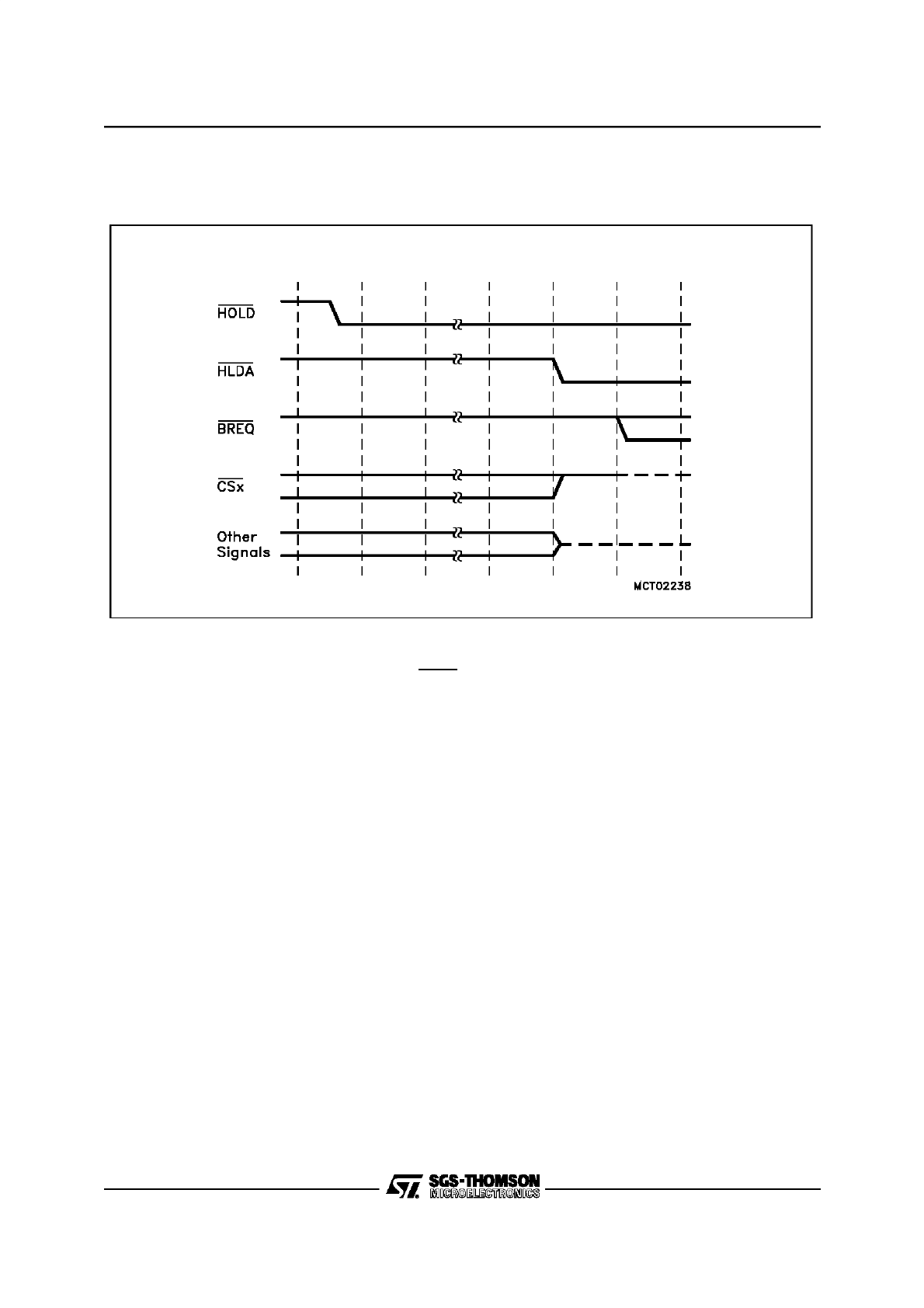
22/24
7 - EXTERNAL BUS INTERFACE (ST10R163)
EXTERNAL BUS ARBITRATION(Cont’d)
Figure 4-11. External Bus Arbitration, Releasing the Bus
Note: The ST10R163 will complete the currently running bus cycle before granting bus access as indicated by the broken
lines. This may delay hold acknowledge compared to this figure.
The figure above shows the first possibility for BREQ to get active.
128
23/24
7 - EXTERNAL BUS INTERFACE (ST10R163)
EXTERNAL BUS ARBITRATION(Cont’d)
Exiting the Hold State
The external bus master returns the access rights
to the ST10R163 by driving theHOLD input high.
After synchronizing this signal the ST10R163 will
drive the HLDA output high, actively drive the con-
trol signals and resume executing external bus cy-
cles if required.
Depending on the arbitration logic, the external
bus can be returned to the ST10R163 under two
circumstances:
•
The external master does no more require ac-
cess to the shared resources and gives up its own
access rights, or
•
The ST10R163 needs access to the shared re-
sources and demands this by activating itsBREQ
output. The arbitration logic may then deactivate
the other master’s HLDA and so free the external
bus for the ST10R163, depending on the priority
of the different masters.
Figure 4-12. External Bus Arbitration, (Regaining the Bus)
Note: The falling BREQ edge shows the last chance for BREQ to trigger the indicated regain-sequence. Even if BREQ
is activated earlier the regain-sequence is initiated by HOLD going high. BREQ and HOLD are connected via an
external arbitration circuitry. Please note that HOLD may also be deactivated without the ST10R163 requesting the
bus.
129

24/24
7 - EXTERNAL BUS INTERFACE (ST10R163)
7.8 THE XBUS INTERFACE
The ST10R163 provides an on-chip interface (the
XBUS interface), which allows to connect integrat-
ed customer/application specific peripherals to the
standard controller core. The XBUS is an internal
representation of the external bus interface, ie. it is
operated in the same way.
The current XBUS interface is prepared to support
up to 3 X-Peripherals.
For each peripheral on the XBUS (X-Peripheral)
there is a separate address window controlled by
an XBCON and an XADRS register. As an inter-
face to a peripheral in many cases is represented
by just a few registers, the XADRS registers select
smaller address windows than the standard AD-
DRSEL registers. As the register pairs control in-
tegrated peripherals rather than externally con-
nected ones, they are fixed by mask programming
rather than being user programmable.
X-Peripheral accesses provide the same choices
as external accesses, so these peripherals may
be bytewide or wordwide, with or without a sepa-
rate address bus. Interrupt nodes and configura-
tion pins (on PORT0) are provided for X-Peripher-
als to be integrated.
Note: If you plan to develop a peripheral of your
own to be integrated into a ST10R163 device to
create a customer specific version, please ask for
the specification of the XBUS interface and for fur-
ther support.
130
February 1996
1/28
This is advance information from SGS-TH OMSON. Details are subject tochange without notice.
ST10R163
User Manual
8 - GENERAL PURPOSE TIMER UNITS
The General Purpose Timer Units GPT1 and
GPT2 represent very flexible multifunctional timer
structures which may be used for timing, event
counting, pulse width measurement, pulse gener-
ation, frequency multiplication, and other purpos-
es. They incorporate five 16-bit timers that are
grouped into the two timer blocks GPT1 and
GPT2.
Block GPT1 contains 3 timers/counters with a
maximum resolution of 400 ns (@ 20 MHz CPU
clock),
while
block
GPT2
contains
2
tim-
ers/counters with a maximum resolution of 200 ns
(@ 20 MHz CPU clock) and a 16-bit Capture/Re-
load register (CAPREL). Each timer in each block
may operate independently in a number of differ-
ent modes such as gated timer or counter mode,
or may be concatenated with another timer of the
same block. The auxiliary timers of GPT1 may op-
tionally be configured as reload or capture regis-
ters for the core timer. In the GPT2 block, the ad-
ditional CAPREL register supports capture and re-
load operation with extended functionality. Each
block has alternate input/output functions and
specific interrupts associated with it.
8.1 TIMER BLOCK GPT1
From a programmer’s point of view, the GPT1
block is composed of a set of SFRs as summa-
rized below. Those portions of port and direction
registers which are used for alternate functions by
the GPT1 block are shaded.
Figure 5-1. SFRs and Port Pins Associated with Timer Block GPT1
T4IC
T2
GPT1 Timer 2 Register
T3
GPT1 Timer 3 Register
T4
GPT1 Timer 4 Register
T2IC
GPT1 Timer 2 Interrupt Control Register
T3IC
GPT1 Timer 3 Interrupt Control Register
T4IC
GPT1 Timer 4 Interrupt Control Register
T2IN/P3.7
T2EUD/P5.15
T3IN/P3.6
T3EUD/P3.4
T4IN/P3.5
T4EUD/P5.14
T3OUT/P 3.3
T2CON
Ports & Direction Control
Alternate Functions
Data Registers
Control Registers
Interrupt Control
T2
T2IC
DP3
P3
T3
T4
T3IC
T3CON
T4CON
P5
ODP3
ODP3
Port 3 Open Drain Control Register
DP3
Port 3 Direction Control Register
P3
Port 3 Data Register
T2CON
GPT1 Timer 2 Control Register
T3CON
GPT1 Timer 3 Control Register
T4CON
GPT1 Timer 4 Control Register
131
2/28
8 - GENERAL PURPOSE TIMER UNITS (ST10R163)
TIMER BLOCK GPT1 (Cont’d)
All three timers of block GPT1 (T2, T3, T4) can run
in 3 basic modes, which are timer, gated timer,
and counter mode, and all timers can either count
up or down. Each timer has an alternate input
function pin on Port 3 associated with it which
serves as the gate control in gated timer mode, or
as the count input in counter mode. The count di-
rection (Up / Down) may be programmed via soft-
ware or may be dynamically altered by a signal at
an external control input pin. Each overflow/under-
flow of core timer T3 may be indicated on an alter-
nate output function pin. The auxiliary timers T2
and T4 may additionally be concatenated with the
core timer, or used as capture or reload registers
for the core timer.
The current contents of each timer can be read or
modified by the CPU by accessing the corre-
sponding timer registers T2, T3, or T4, which are
located in the non-bitaddressable SFR space.
When any of the timer registers is written to by the
CPU in the state immediately before a timer incre-
ment, decrement, reload, or capture is to be per-
formed, the CPU write operation has priority in or-
der to guarantee correct results.
Figure 5-2. GPT1 Block Diagram
132
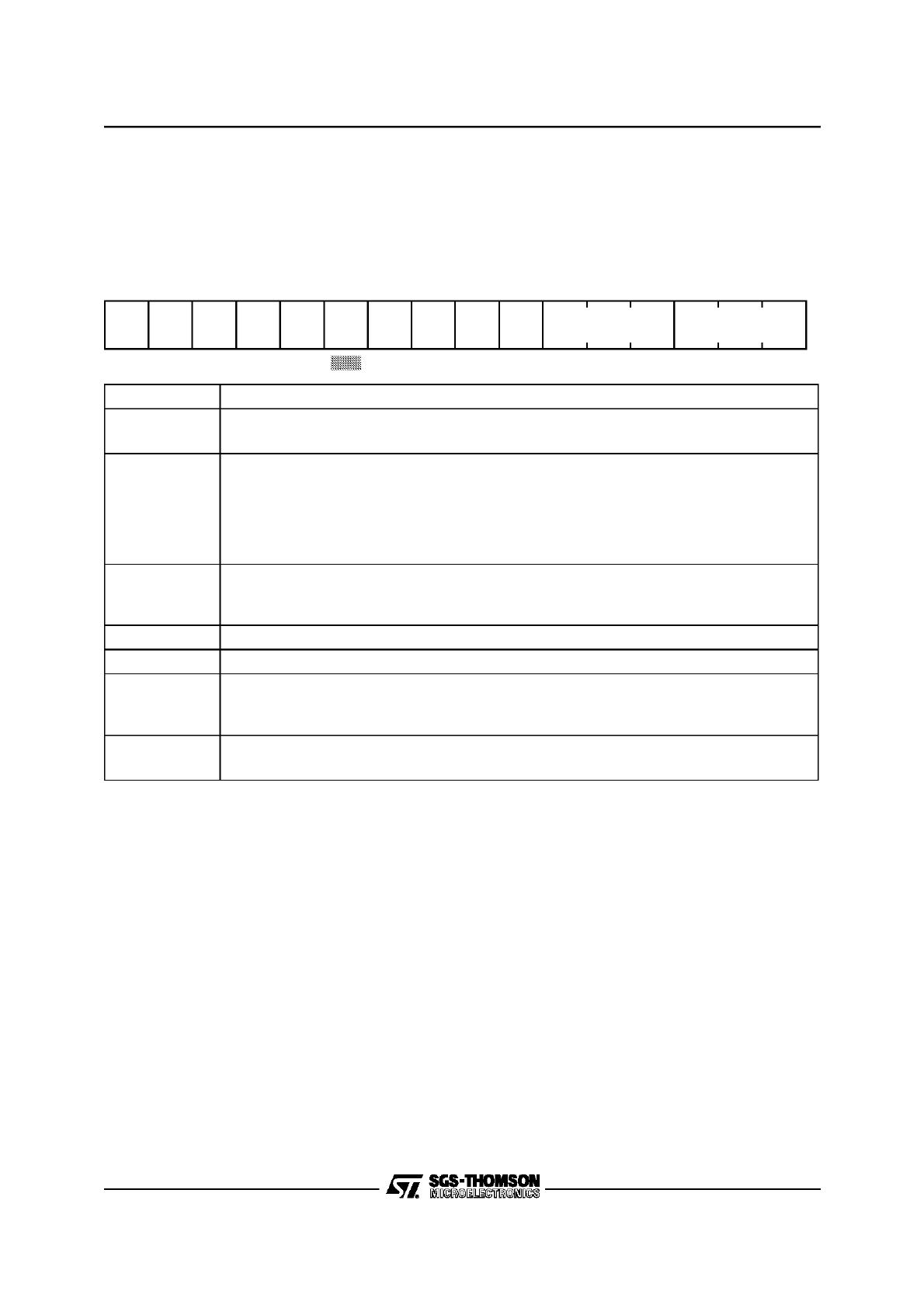
3/28
8 - GENERAL PURPOSE TIMER UNITS (ST10R163)
TIMER BLOCK GPT1 (Cont’d)
8.1.1 GPT1 Core Timer T3
The core timer T3 is configured and controlled via its bitaddressable control register T3CON.
T3CON (FF42h / A1h)
SFR
Reset Value: 0000h
*)
For the effects of bits T3UD and T3UDE refer to the direction table below.
Bit
Function
T3I
Timer 3 Input Selection
Depends on the operating mode, see respective sections.
T3M
Timer 3 Mode Control (Basic Operating Mode)
0 0 0 :Timer Mode
0 0 1 :Counter Mode
0 1 0 :Gated Timer with Gate active low
0 1 1 :Gated Timer with Gate active high
1 X X :Reserved. Do not use this combination.
T3R
Timer 3 Run Bit
T3R = ‘0’:Timer / Counter 3 stops
T3R = ‘1’:Timer / Counter 3 runs
T3UD
Timer 3 Up / Down Control
*)
T3UDE
Timer 3 External Up/Down Enable
*)
T3OE
Alternate Output Function Enable
T3OE = ‘0’:Alternate Output Function Disabled
T3OE = ‘1’:Alternate Output Function Enabled
T3OTL
Timer 3 Output Toggle Latch
Toggles on each overflow / underflow of T3. Can be set or reset by software.
5
4
3
2
1
0
11
10
9
8
7
6
15
14
13
12
rw
rw
-
rw
rw
rw
rw
rw
-
-
-
-
T3R
T3UD
T3OE
-
-
-
-
-
T3
OTL
T3
UDE
T3M
T3I
133
4/28
8 - GENERAL PURPOSE TIMER UNITS (ST10R163)
TIMER BLOCK GPT1 (Cont’d)
Timer 3 Run Bit
The timer can be started or stopped by software
through bit T3R (Timer T3 Run Bit). If T3R=‘0’, the
timer stops. Setting T3R to ‘1’ will start the timer.
In gated timer mode, the timer will only run if
T3R=‘1’ and the gate is active (high or low, as pro-
grammed).
Count Direction Control
The count direction of the core timer can be con-
trolled either by software or by the external input
pin T3EUD (Timer T3 External Up/Down Control
Input), which is the alternate input function of port
pin P3.4. These options are selected by bits T3UD
and T3UDE in control register T3CON. When the
up/down
control
is
done
by
software
(bit
T3UDE=‘0’), the count direction can be altered by
setting or clearing bit T3UD. When T3UDE=‘1’, pin
T3EUD is selected to be the controlling source of
the count direction. However, bit T3UD can still be
used to reverse the actual count direction, as
shown in the table below. If T3UD=‘0’ and pin
T3EUD shows a low level, the timer is counting
up. With a high level at T3EUD the timer is count-
ing down. If T3UD=‘1’, a high level at pin T3EUD
specifies counting up, and a low level specifies
counting down. The count direction can be
changed regardless of whether the timer is run-
ning or not.
When pin T3EUD/P3.4 is used as external count
direction control input, it must be configured as in-
put, ie. its corresponding direction control bit
DP3.4 must be set to ‘0’.
Timer 3 Output Toggle Latch
An overflow or underflow of timer T3 will clock the
toggle bit T3OTL in control register T3CON.
T3OTL can also be set or reset by software. Bit
T3OE (Alternate Output Function Enable) in regis-
ter T3CON enables the state of T3OTL to be an al-
ternate
function
of
the
external output
pin
T3OUT/P3.3. For that purpose, a ‘1’ must be writ-
ten into port data latch P3.3 and pin T3OUT/P3.3
must be configured as output by setting direction
control bit DP3.3 to ‘1’. If T3OE=‘1’, pin T3OUT
then outputs the state of T3OTL. If T3OE=‘0’, pin
T3OUT can be used as general purpose IO pin.
In addition, T3OTL can be used in conjunction
with the timer over/underflows as an input for the
counter function or as a trigger source for the re-
load function of the auxiliary timers T2 and T4. For
this purpose, the state of T3OTL does not have to
be available at pin T3OUT, because an internal
connection is provided for this option.
GPT1 Core Timer T3 Count Direction Control
Note: The direction control works the same for core timer T3 and for auxiliary timers T2 and T4. Therefore the pins and
bits are named Tx...
Pin TxEUD
Bit TxUDE
Bit TxUD
Count Direction
X
0
0
Count Up
X
0
1
Count Down
0
1
0
Count Up
1
1
0
Count Down
0
1
1
Count Down
1
1
1
Count Up
134
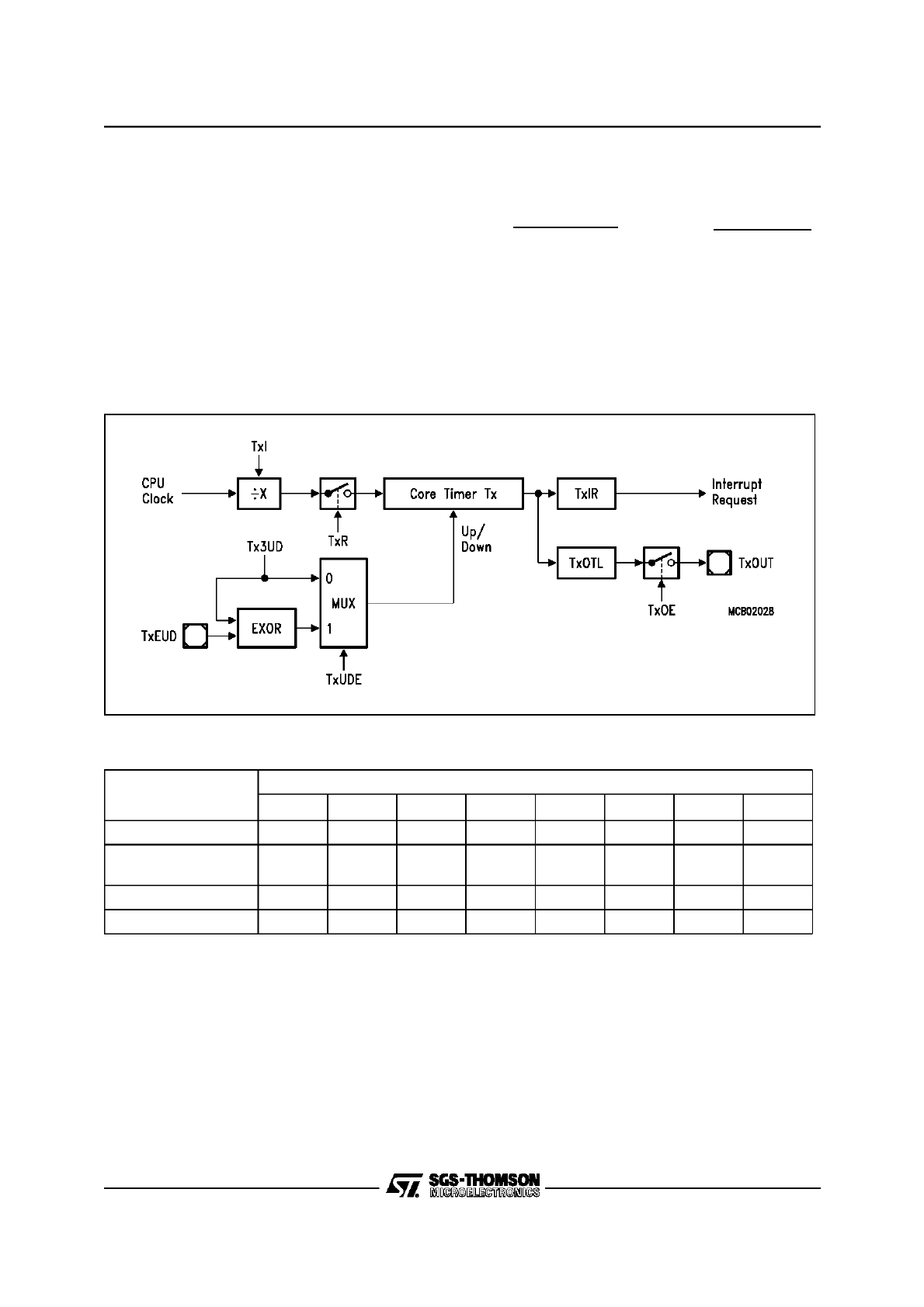
5/28
8 - GENERAL PURPOSE TIMER UNITS (ST10R163)
TIMER BLOCK GPT1 (Cont’d)
Timer 3 in Timer Mode
Timer mode for the core timer T3 is selected by
setting bit field T3M in register T3CON to ‘000b’. In
this mode, T3 is clocked with the internal system
clock (CPU clock) divided by a programmable
prescaler, which is selected by bit field T3I. The in-
put frequency
f
T3
for timer T3 and its resolution r
T3
are scaled linearly with lower clock frequencies
f
CPU
, as can be seen from the following formula:
The timer input frequencies, resolution and peri-
ods which result from the selected prescaler op-
tion when using a 20 MHz CPU clock are listed in
the table below. This table also applies to the Gat-
ed Timer Mode of T3 and to the auxiliary timers T2
and T4 in timer and gated timer mode. Note that
some numbers may be rounded to 3 significant
digits.
Figure 5-3. Block Diagram of Core Timer T3 in Timer Mode
GPT1 Timer Input Frequencies, Resolution and Periods
f
T3
=
f
CPU
8 * 2
<T3I>
r
T3
[
µ
s] =
f
CPU
[MHz]
8 * 2
<T3I>
T3EUD
=
P3.4
T3OUT
=
P3.3
x = 3
f
CPU
= 20MHz
Timer Input Selection T2I / T3I / T4I
000b
001b
010b
011b
100b
101b
110b
111b
Prescaler factor
8
16
32
64
128
256
512
1024
Input Frequency
2.5
MHz
1.25
MHz
625
kHz
312.5
kHz
156.25
kHz
78.125
kHz
39.06
kHz
19.53
kHz
Resolution
400 ns
800 ns
1.6
µ
s
3.2
µ
s
6.4
µ
s
12.8
µ
s
25.6
µ
s
51.2
µ
s
Period
26 ms
52.5 ms
105 ms
210 ms
420 ms
840 ms
1.68 s
3.36 s
135
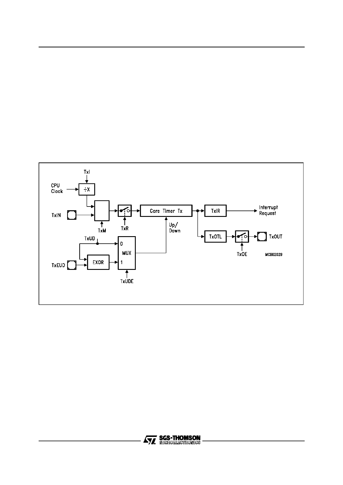
6/28
8 - GENERAL PURPOSE TIMER UNITS (ST10R163)
TIMER BLOCK GPT1 (Cont’d)
Timer 3 in Gated Timer Mode
Gated timer mode for the core timer T3 is selected
by setting bit field T3M in register T3CON to ‘010b’
or ‘011b’. Bit T3M.0 (T3CON.3) selects the active
level of the gate input. In gated timer mode the
same options for the input frequency as for the
timer mode are available. However, the input
clock to the timer in this mode is gated by the ex-
ternal input pin T3IN (Timer T3 External Input),
which is an alternate function of P3.6.
To enable this operation pin T3IN/P3.6 must be
configured as input, ie. direction control bit DP3.6
must contain ‘0’.
If T3M.0=‘0’, the timer is enabled when T3IN
shows a low level. A high level at this pin stops the
timer. If T3M.0=‘1’, pin T3IN must have a high lev-
el in order to enable the timer. In addition, the tim-
er can be turned on or off by software using bit
T3R. The timer will only run, if T3R=‘1’ and the
gate is active. It will stop, if either T3R=‘0’ or the
gate is inactive.
Note: A transition of the gate signal at pin T3IN
does not cause an interrupt request.
Figure 5-4. Block Diagram of Core Timer T3 in Gated Timer Mode
T3IN
=
P3.6
T3EUD
=
P3.4
T3OUT
=
P3.3
x = 3
136
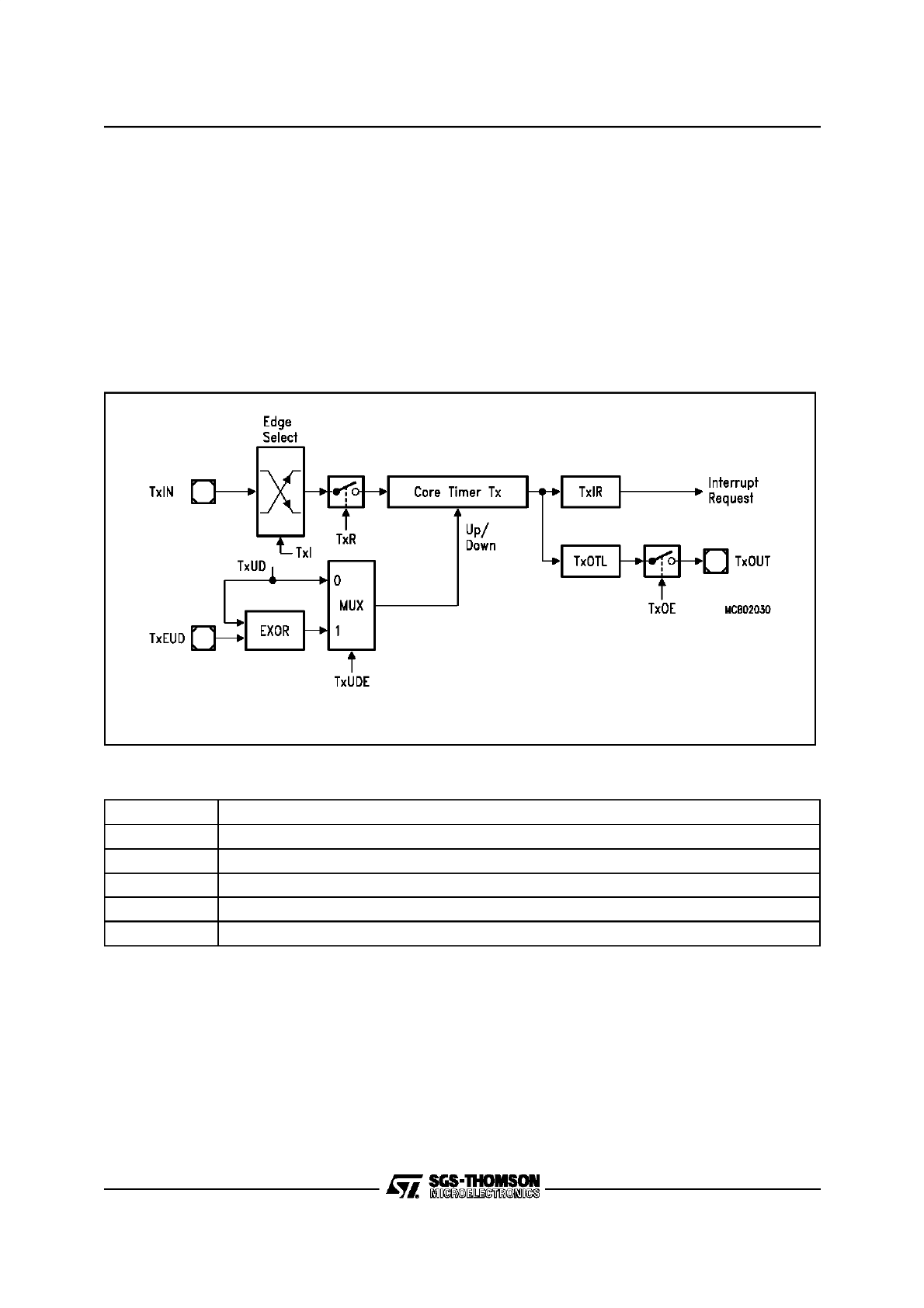
7/28
8 - GENERAL PURPOSE TIMER UNITS (ST10R163)
TIMER BLOCK GPT1 (Cont’d)
Timer 3 in Counter Mode
Counter mode for the core timer T3 is selected by
setting bit field T3M in register T3CON to ‘001b’. In
counter mode timer T3 is clocked by a transition at
the external input pin T3IN, which is an alternate
function of P3.6. The event causing an increment
or decrement of the timer can be a positive, a neg-
ative, or both a positive and a negative transition
at this pin. Bit field T3I in control register T3CON
selects the triggering transition (see table below).
For counter operation, pin T3IN/P3.6 must be con-
figured as input, ie. direction control bit DP3.6
must be ‘0’. The maximum input frequency which
is allowed in counter mode is
f
CPU
(1.25 MHz @
f
CPU
= 20 MHz). To ensure that a transition of the
count input signal which is applied to T3IN is cor-
rectly recognized, its level should be held high or
low for at least 8
f
CPU
cycles before it changes.
Figure 5-5. Block Diagram of Core Timer T3 in Counter Mode
GPT1 Core Timer T3 (Counter Mode) Input Edge Selection
T3IN
=
P3.6
T3EUD
=
P3.4
T3OUT
=
P3.3
x = 3
T3I
Trigg ering Edge for Count er Increment / Decrement
0 0 0
None. Counter T3 is disabled
0 0 1
Positive transition (rising edge) on T3IN
0 1 0
Negative transition (falling edge) on T3IN
0 1 1
Any transition (rising or falling edge) on T3IN
1 X X
Reserved. Do not use this combination
137
8/28
8 - GENERAL PURPOSE TIMER UNITS (ST10R163)
TIMER BLOCK GPT1 (Cont’d)
8.1.2 GPT1 Auxiliary Timers T2 and T4
Both auxiliary timers T2 and T4 have exactly the
same functionality. They can be configured for
timer, gated timer, or counter mode with the same
options for the timer frequencies and the count
signal as the core timer T3. In addition to these 3
counting modes, the auxiliary timers can be con-
catenated with the core timer, or they may be used
as reload or capture registers in conjunction with
the core timer.
Note: The auxiliary timers have no output toggle
latch and no alternate output function.
The individual configuration for timers T2 and T4
is determined by their bitaddressable control reg-
isters T2CON and T4CON, which are both organ-
ized identically. Note that functions which are
present in all 3 timers of block GPT1 are controlled
in the same bit positions and in the same manner
in each of the specific control registers.
T2CON (FF40h / A0h)
SFR
Reset Value: 0000h
T4CON (FF44h / A2h)
SFR
Reset Value: 0000h
*)
For the effects of bits TxUD and TxUDE refer to the direction table (see T3 section).
Bit
Function
TxI
Timer x Input Selection
Depends on the Operating Mode, see respective sections.
TxM
Timer x Mode Control (Basic Operating Mode)
0 0 0 :Timer Mode
0 0 1 :Counter Mode
0 1 0 :Gated Timer with Gate active low
0 1 1 :Gated Timer with Gate active high
1 0 0 :Reload Mode
1 0 1 :Capture Mode
1 1 X :Reserved. Do not use this combination
TxR
Timer x Run Bit
TxR = ‘0’:Timer / Counter x stops
TxR = ‘1’:Timer / Counter x runs
TxUD
Timer x Up / Down Control
*)
TxUDE
Timer x External Up/Down Enable
*)
5
4
3
2
1
0
11
10
9
8
7
6
15
14
13
12
rw
rw
-
-
-
rw
rw
rw
-
-
-
-
T2R
T2UD
-
-
-
-
-
T2
UDE
-
-
T2I
T2M
5
4
3
2
1
0
11
10
9
8
7
6
15
14
13
12
rw
rw
-
-
-
rw
rw
rw
-
-
-
-
T4R
T4UD
-
-
-
-
-
T4
UDE
-
-
T4I
T4M
138
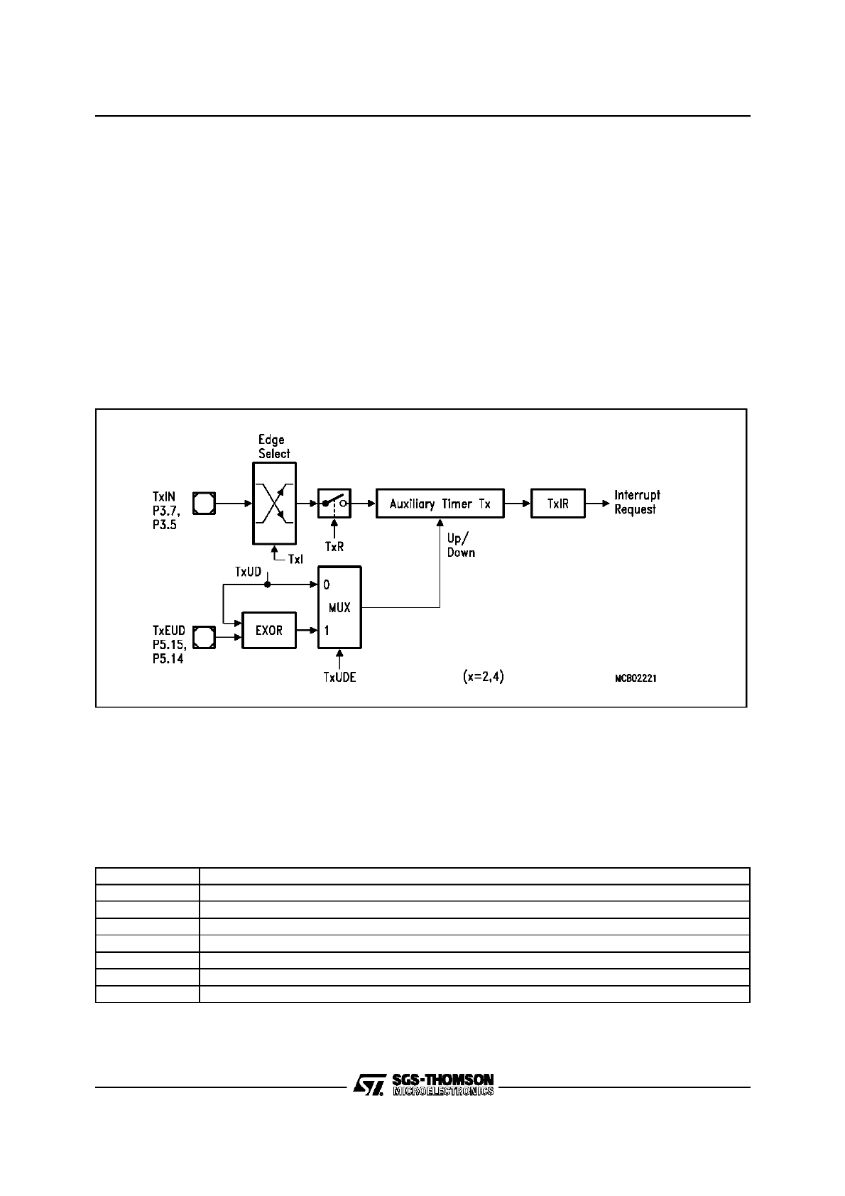
9/28
8 - GENERAL PURPOSE TIMER UNITS (ST10R163)
TIMER BLOCK GPT1 (Cont’d)
Count Direction Control for Auxiliary Timers
The count direction of the auxiliary timers can be
controlled in the same way as for the core timer
T3. The description and the table apply according-
ly.
Timers T2 and T4 in Timer Mode or Gated Tim-
er Mode
When the auxiliary timers T2 and T4 are pro-
grammed to timer mode or gated timer mode, their
operation is the same as described for the core
timer T3. The descriptions, figures and tables ap-
ply accordingly with one exception:
•
There is no output toggle latch and no alternate
output pin for T2 and T4.
Timers T2 and T4 in Counter Mode
Counter mode for the auxiliary timers T2 and T4 is
selected by setting bit field TxM in the respective
register TxCON to ‘001b’. In counter mode timers
T2 and T4 can be clocked either by a transition at
the respective external input pin TxIN, or by a tran-
sition of timer T3’s output toggle latch T3OTL.
Figure 5-6. Block Diagram of an Auxiliary Timer in Counter Mode
The event causing an increment or decrement of a
timer can be a positive, a negative, or both a pos-
itive and a negative transition at either the respec-
tive input pin, or at the toggle latch T3OTL.
Bit field TxI in the respective control register Tx-
CON selects the triggering transition (see table
below).
For counter operation, pin TxIN must be config-
ured as input, ie. the respective direction control
bit must be ‘0’. The maximum input frequency
which is allowed in counter mode is
f
CPU/8
(1.25
MHz @
f
CPU
=20 MHz). To ensure that a transition
of the count input signal which is applied to TxIN is
correctly recognized, its level should be held for at
least 8
f
CPU
cycles before it changes.
GPT1 Auxiliary Timer (Counter Mode) Input Edge Selection
Note: Only state transitions of T3OTL which are caused by the overflows/underflows of T3 will trigger the counter function
of T2/T4. Modifications of T3OTL via software will NOT trigger the counter function of T2/T4.
x = 2,4
T2I / T4I
Trigg ering Edge for Count er Increment / Decrement
X 0 0
None. Counter Tx is disabled
0 0 1
Positive transition (rising edge) on TxIN
0 1 0
Negative transition (falling edge) on TxIN
0 1 1
Any transition (rising or falling edge) on TxIN
1 0 1
Positive transition (rising edge) of output toggle latch T3OTL
1 1 0
Negative transition (falling edge) of output toggle latch T3OTL
1 1 1
Any transition (rising or falling edge) of output toggle latch T3OTL
139
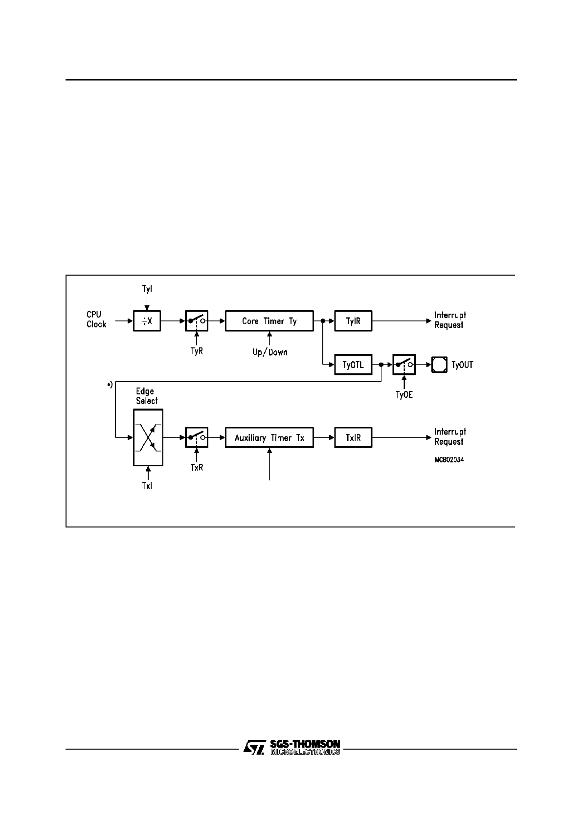
10/28
8 - GENERAL PURPOSE TIMER UNITS (ST10R163)
TIMER BLOCK GPT1 (Cont’d)
Timer Concatenation
Using the toggle bit T3OTL as a clock source for
an auxiliary timer in counter mode concatenates
the core timer T3 with the respective auxiliary tim-
er. Depending on which transition of T3OTL is se-
lected to clock the auxiliary timer, this concatena-
tion forms a 32-bit or a 33-bit timer / counter.
•
32-bit Timer/Counter: If both a positive and a
negative transition of T3OTL is used to clock the
auxiliary timer, this timer is clocked on every over-
flow/underflow of the core timer T3. Thus, the two
timers form a 32-bit timer.
•
33-bit Timer/Counter: If either a positive or a
negative transition of T3OTL is selected to clock
the auxiliary timer, this timer is clocked on every
second overflow/underflow of the core timer T3.
This configuration forms a 33-bit timer (16-bit core
timer+T3OTL+16-bit auxiliary timer).
The count directions of the two concatenated tim-
ers are not required to be the same. This offers a
wide variety of different configurations.
T3 can operate in timer, gated timer or counter
mode in this case.
Figure 5-7. Concatenation of Core Timer T3 and an Auxiliary Timer
*)
Note: Line only affected by over/underflows of T3, but NOT by software modifications of T3OTL.
T3OUT
=
P3.3
x = 2,4 y = 3
140
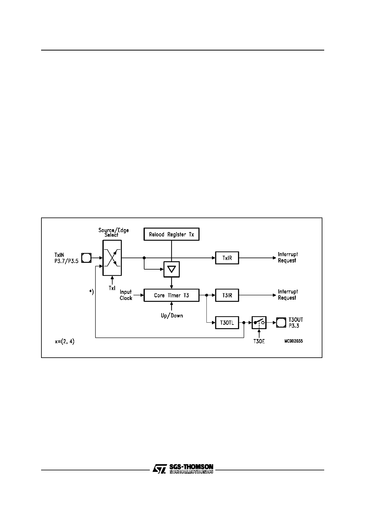
11/28
8 - GENERAL PURPOSE TIMER UNITS (ST10R163)
TIMER BLOCK GPT1 (Cont’d)
Auxiliary Timer in Reload Mode
Reload mode for the auxiliary timers T2 and T4 is
selected by setting bit field TxM in the respective
register TxCON to ‘100b’. In reload mode the core
timer T3 is reloaded with the contents of an auxil-
iary timer register, triggered by one of two different
signals. The trigger signal is selected the same
way as the clock source for counter mode (see ta-
ble above), ie. a transition of the auxiliary timer’s
input or the output toggle latch T3OTL may trigger
the reload.
Note: When programmed for reload mode, the re-
spective auxiliary timer (T2 or T4) stops independ-
ent of its run flag T2R or T4R.
Upon a trigger signal T3 is loaded with the con-
tents of the respective timer register (T2 or T4)
and the interrupt request flag (T2IR or T4IR) is set.
Note: When a T3OTL transition is selected for the
trigger signal, also the interrupt request flag T3IR
will be set upon a trigger, indicating T3’s overflow
or underflow.
Modifications of T3OTL via software will NOT trig-
ger the counter function of T2/T4.
The reload mode triggered by T3OTL can be used
in a number of different configurations. Depending
on the selected active transition the following func-
tions can be performed:
•
If both a positive and a negative transition of
T3OTL is selected to trigger a reload, the core tim-
er will be reloaded with the contents of the auxilia-
ry timer each time it overflows or underflows. This
is the standard reload mode (reload on over-
flow/underflow).
•
If either a positive or a negative transition of
T3OTL is selected to trigger a reload, the core tim-
er will be reloaded with the contents of the auxilia-
ry timer on every second overflow or underflow.
Figure 5-8. GPT1 Auxiliary Timer in Reload Mode
*)
Note: Line only affected by over/underflows of T3, but NOT by software modifications of T3OTL.
141
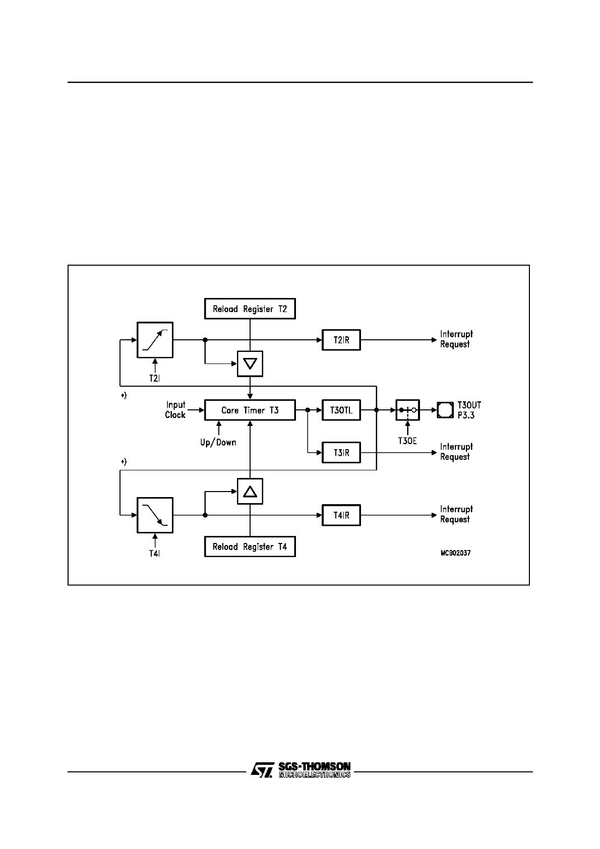
12/28
8 - GENERAL PURPOSE TIMER UNITS (ST10R163)
TIMER BLOCK GPT1 (Cont’d)
•
Using this “single-transition” mode for both auxil-
iary timers allows to perform very flexible pulse
width modulation (PWM). One of the auxiliary tim-
ers is programmed to reload the core timer on a
positive transition of T3OTL, the other is pro-
grammed for a reload on a negative transition of
T3OTL. With this combination the core timer is al-
ternately reloaded from the two auxiliary timers.
The figure below shows an example for the gener-
ation of a PWM signal using the alternate reload
mechanism. T2 defines the high time of the PWM
signal (reloaded on positive transitions) and T4
defines the low time of the PWM signal (reloaded
on negative transitions). The PWM signal can be
output on T3OUT with T3OE=‘1’, P3.3=‘1’ and
DP3.3=‘1’. With this method the high and low time
of the PWM signal can be varied in a wide range.
Note: The output toggle latch T3OTL is accessible
via software and may be changed, if required, to
modify the PWM signal. However, this will NOT
trigger the reloading of T3.
Figure 5-9. GPT1 Timer Reload Configuration for PWM Generation
Note: Although it is possible, it should be avoided to select the same reload trigger event for both auxiliary timers. In this
case both reload registers would try to load the core timer at the same time. If this combination is selected, T2 is
disregarded and the contents of T4 is reloaded.
*) Note: Lines only affected by over/underflows of T3, but NOT by software modifications of T3OTL.
142
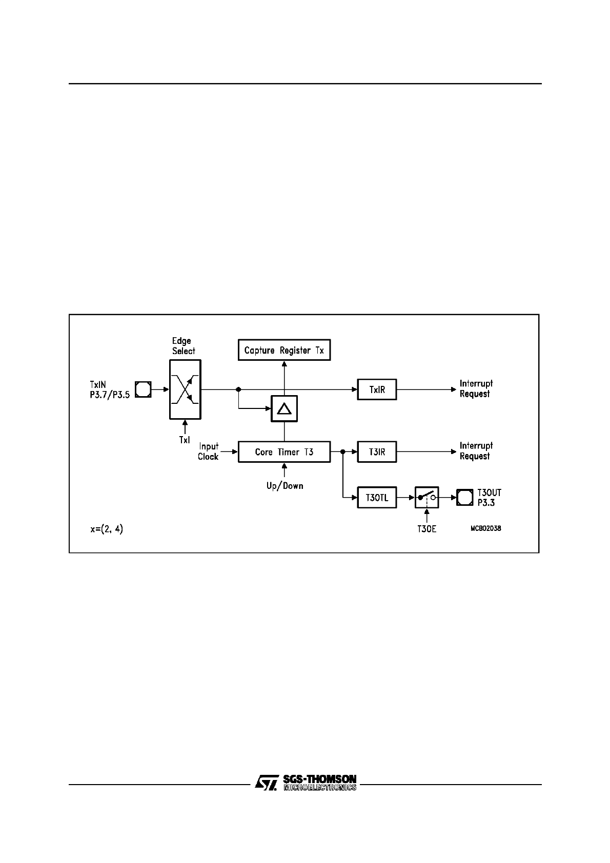
13/28
8 - GENERAL PURPOSE TIMER UNITS (ST10R163)
TIMER BLOCK GPT1 (Cont’d)
Auxiliary Timer in Capture Mode
Capture mode for the auxiliary timers T2 and T4 is
selected by setting bit field TxM in the respective
register TxCON to ‘101b’. In capture mode the
contents of the core timer are latched into an aux-
iliary timer register in response to a signal transi-
tion at the respective auxiliary timer’s external in-
put pin TxIN. The capture trigger signal can be a
positive, a negative, or both a positive and a neg-
ative transition.
The two least significant bits of bit field TxI are
used to select the active transition (see table in the
counter mode section), while the most significant
bit TxI.2 is irrelevant for capture mode. It is recom-
mended to keep this bit cleared (TxI.2 = ‘0’).
Note: When programmed for capture mode, the
respective auxiliary timer (T2 or T4) stops inde-
pendent of its run flag T2R or T4R.
Upon a trigger (selected transition) at the corre-
sponding input pin TxIN the contents of the core
timer are loaded into the auxiliary timer register
and the associated interrupt request flag TxIR will
be set.
Note: The direction control bits DP3.7 (for T2IN)
and DP3.5 (for T4IN) must be set to ’0’, and the
level of the capture trigger signal should be held
high or low for at least 8 f
CPU
cycles before it
changes to ensure correct edge detection.
Figure 5-10. GPT1 Auxiliary Timer in Capture Mode
143
14/28
8 - GENERAL PURPOSE TIMER UNITS (ST10R163)
TIMER BLOCK GPT1 (Cont’d)
8.1.3 Interrupt Control for GPT1 Timers
When a timer overflows from FFFFh to 0000h
(when counting up), or when it underflows from
0000h to FFFFh (when counting down), its inter-
rupt request flag (T2IR, T3IR or T4IR) in register
TxIC will be set. This will cause an interrupt to the
respective timer interrupt vector (T2INT, T3INT or
T4INT) or trigger a PEC service, if the respective
interrupt enable bit (T2IE, T3IE or T4IE in register
TxIC) is set. There is an interrupt control register
for each of the three timers.
T2IC (FF60h / B0h)
SFR
Reset Value: - - 00h
T3IC (FF62h / B1h)
SFR
Reset Value: - - 00h
T4IC (FF64h / B2h)
SFR
Reset Value: - - 00h
Note: Please refer to the general Interrupt Control Register description for an explanation of the control fields.
5
4
3
2
1
0
11
10
9
8
7
6
15
14
13
12
rw
rw
-
-
-
-
rw
rw
-
-
-
-
T2IE
T2IR
GLVL
ILVL
5
4
3
2
1
0
11
10
9
8
7
6
15
14
13
12
rw
rw
-
-
-
-
rw
rw
-
-
-
-
T3IE
T3IR
GLVL
ILVL
5
4
3
2
1
0
11
10
9
8
7
6
15
14
13
12
rw
rw
-
-
-
-
rw
rw
-
-
-
-
T4IE
T4IR
GLVL
ILVL
144
15/28
8 - GENERAL PURPOSE TIMER UNITS (ST10R163)
8.2 TIMER BLOCK GPT2
From a programmer’s point of view, the GPT2
block is represented by a set of SFRs as summa-
rized below. Those portions of port and direction
registers which are used for alternate functions by
the GPT2 block are shaded.
Timer block GPT2 supports high precision event
control with a maximum resolution of 200 ns (@
20 MHz CPU clock). It includes the two timers T5
and T6, and the 16-bit capture/reload register
CAPREL. Timer T6 is referred to as the core timer,
and T5 is referred to as the auxiliary timer of
GPT2.
Each timer has an alternate input function pin as-
sociated with it which serves as the gate control in
gated timer mode, or as the count input in counter
mode. The count direction (Up / Down) may be
programmed via software or may be dynamically
altered by a signal at an external control input pin.
An overflow/underflow of T6 is indicated by the
output toggle bit T6OTL whose state may be out-
put on an alternate function port pin. In addition,
T6 may be reloaded with the contents of CAPREL.
The toggle bit also supports the concatenation of
T6 with auxiliary timer T5. Triggered by an exter-
nal signal, the contents of T5 can be captured into
register CAPREL, and T5 may optionally be
cleared. Both timer T6 and T5 can count up or
down, and the current timer value can be read or
modified by the CPU in the non-bitaddressable
SFRs T5 and T6.
Figure 5-11. SFRs and Port Pins Associated with Timer Block GPT2
ODP3
Port 3 Open Drain Control Register
DP3
Port 3 Direction Control Register
P3
Port 3 Data Register
P5
Port 5 Data Register
T5CON
GPT2 Timer 5 Control Register
T6CON
GPT2 Timer 6 Control Register
T5IN/P 5.13
T5EUD/P 5.11
T6IN/P 5.12
T6EUD/P 5.10
CAPI N/P3.2
T6OUT/P 3.1
T5CON
Control Registers
T5
GPT2 Timer 5 Register
T6
GPT2 Timer 6 Register
CAPREL
GPT2 Capture/Reload Register
T5IC
GPT2 Timer 5 Interrupt Control Register
T6IC
GPT2 Timer 6 Interrupt Control Register
CRIC
GPT2 CAPREL Interrupt Control Register
Ports & Direction Control
Alternate Functions
Data Registers
Control Registers
Interrupt Control
T5
T5IC
DP3
P3
T6
CAPREL
T6IC
CRIC
T6CON
P5
ODP3
145
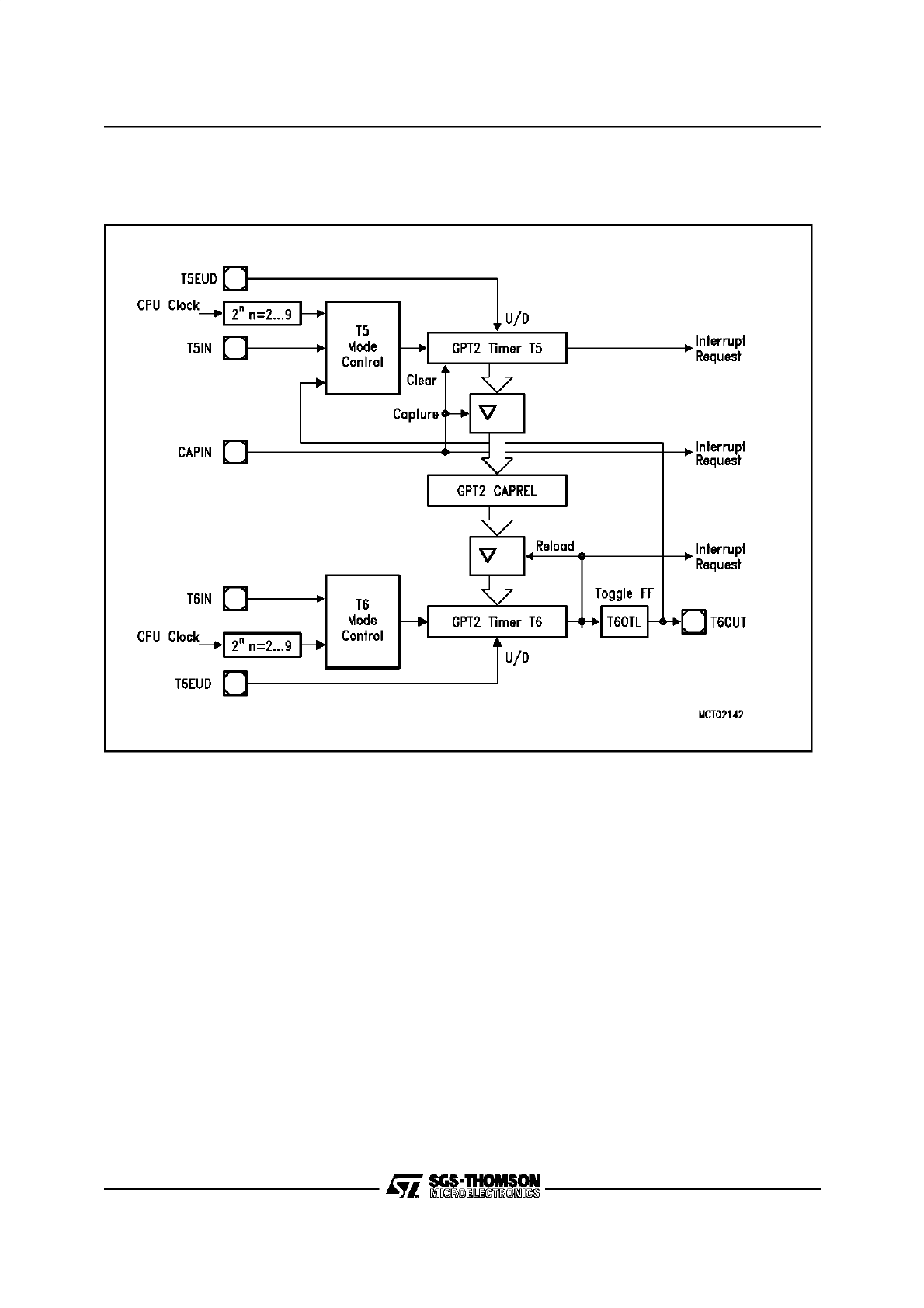
16/28
8 - GENERAL PURPOSE TIMER UNITS (ST10R163)
TIMER BLOCK GPT1 (Cont’d)
Figure 5-12. GPT2 Block Diagram
146
17/28
8 - GENERAL PURPOSE TIMER UNITS (ST10R163)
TIMER BLOCK GPT1 (Cont’d)
8.2.1 GPT2 Core Timer T6
The operation of the core timer T6 is controlled by
its bitaddressable control register T6CON.
Timer 6 Run Bit
The timer can be started or stopped by software
through bit T6R (Timer T6 Run Bit). If T6R=‘0’, the
timer stops. Setting T6R to ‘1’ will start the timer.
In gated timer mode, the timer will only run if
T6R=‘1’ and the gate is active (high or low, as pro-
grammed).
T6CON (FF48h / A4h)
SFR
Reset Value: 0000h
*)
For the effects of bits T6UD and T6UDE refer to the direction table below.
Bit
Functio n
T6I
Timer 6 Input Selection
Depends on the Operating Mode, see respective sections.
T6M
Timer 6 Mode Control (Basic Operating Mode)
0 0 0 :Timer Mode
0 0 1 :Counter Mode
0 1 0 :Gated Timer with Gate active low
0 1 1 :Gated Timer with Gate active high
1 X X :Reserved. Do not use this combination.
T6R
Timer 6 Run Bit
T6R = ‘0’:Timer / Counter 6 stops
T6R = ‘1’:Timer / Counter 6 runs
T6UD
Timer 6 Up / Down Control
*)
T6UDE
Timer 6 External Up/Down Enable
*)
T6OE
Alternate Output Function Enable
T6OE = ‘0’:Alternate Output Function Disabled
T6OE = ‘1’:Alternate Output Function Enabled
T6OTL
Timer 6 Output Togg le Latch
Toggles on each overflow / underflow of T6. Can be set or reset by software.
T6SR
Timer 6 Reload Mode Enable
T6SR = ‘0’:Reload from register CAPREL Disabled
T6SR = ‘1’:Reload from register CAPREL Enabled
5
4
3
2
1
0
11
10
9
8
7
6
15
14
13
12
rw
rw
-
rw
rw
rw
rw
rw
rw
-
-
-
T6R
T6UD
T6OE
-
-
-
-
T6SR
T6
OTL
T6
UDE
T6I
T6M
147
18/28
8 - GENERAL PURPOSE TIMER UNITS (ST10R163)
TIMER BLOCK GPT1 (Cont’d)
Count Direction Control
The count direction of the core timer can be con-
trolled either by software or by the external input
pin T6EUD (Timer T6 External Up/Down Control
Input), which is the alternate input function of port
pin P5.10. These options are selected by bits
T6UD and T6UDE in control register T6CON.
When the up/down control is done by software (bit
T6UDE=‘0’), the count direction can be altered by
setting or clearing bit T6UD. When T6UDE=‘1’, pin
T6EUD is selected to be the controlling source of
the count direction. However, bit T6UD can still be
used to reverse the actual count direction, as
shown in the table below. If T6UD=‘0’ and pin
T6EUD shows a low level, the timer is counting
up. With a high level at T6EUD the timer is count-
ing down. If T6UD=‘1’, a high level at pin T6EUD
specifies counting up, and a low level specifies
counting down. The count direction can be
changed regardless of whether the timer is run-
ning or not.
Timer 6 Output Toggle Latch
An overflow or underflow of timer T6 will clock the
toggle bit T6OTL in control register T6CON.
T6OTL can also be set or reset by software. Bit
T6OE (Alternate Output Function Enable) in regis-
ter T6CON enables the state of T6OTL to be an al-
ternate
function
of
the
external output
pin
T6OUT/P3.1. For that purpose, a ‘1’ must be writ-
ten into port data latch P3.1 and pin T6OUT/P3.1
must be configured as output by setting direction
control bit DP3.1 to ‘1’. If T6OE=‘1’, pin T6OUT
then outputs the state of T6OTL. If T6OE=‘0’, pin
T6OUT can be used as general purpose IO pin.
In addition, T6OTL can be used in conjunction
with the timer over/underflows as an input for the
counter function of the auxiliary timer T5. For this
purpose, the state of T6OTL does not have to be
available at pin T6OUT, because an internal con-
nection is provided for this option.
GPT2 Core Timer T6 Count Direction Control
Note: The direction control works the same for core timer T6 and for auxiliary timer T5. Therefore the pins and bits are
named Tx...
Pin TxEUD
Bit TxUDE
Bit TxUD
Count Direction
X
0
0
Count Up
X
0
1
Count Down
0
1
0
Count Up
1
1
0
Count Down
0
1
1
Count Down
1
1
1
Count Up
148
19/28
8 - GENERAL PURPOSE TIMER UNITS (ST10R163)
TIMER BLOCK GPT1 (Cont’d)
Timer 6 in Timer Mode
Timer mode for the core timer T6 is selected by
setting bit field T6M in register T6CON to ‘000b’. In
this mode, T6 is clocked with the internal system
clock divided by a programmable prescaler, which
is selected by bit field T6I. The input frequency
f
T6
for timer T6 and its resolution r
T6
are scaled linear-
ly with lower clock frequencies f
CPU
, as can be
seen from the following formula:
The timer input frequencies, resolution and peri-
ods which result from the selected prescaler op-
tion when using a 20 MHz CPU clock are listed in
the table below. This table also applies to the Gat-
ed Timer Mode of T6 and to the auxiliary timer T5
in timer and gated timer mode. Note that some
numbers may be rounded to 3 significant digits.
Figure 5-13. Block Diagram of Core Timer T6 in Timer Mode
GPT2 Timer Input Frequencies, Resolution and Periods
f
T6
=
f
CPU
4 * 2
<T6I>
r
T6
[
µ
s] =
f
CPU
[MHz]
4 * 2
<T6I>
T6EUD
=
P5.10
T6OUT
=
P3.1
x = 6
f
CPU
= 20MHz
Timer Input Selection T5I / T6I
000b
001b
010b
011b
100b
101b
110b
111b
Prescaler factor
4
8
16
32
64
128
256
512
Input Frequency
5
MHz
2.5
MHz
1.25
MHz
625
kHz
312.5
kHz
156.25
kHz
78.125
kHz
39.06
kHz
Resolution
200ns
400 ns
800 ns
1.6
µ
s
3.2
µ
s
6.4
µ
s
12.8
µ
s
25.6
µ
s
Period
13 ms
26 ms
52.5 ms
105 ms
210 ms
420 ms
840 ms
1.68 s
149
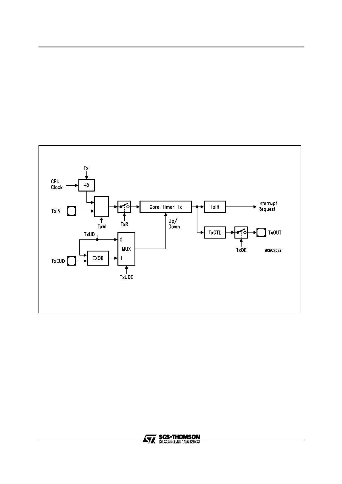
20/28
8 - GENERAL PURPOSE TIMER UNITS (ST10R163)
TIMER BLOCK GPT1 (Cont’d)
Timer 6 in Gated Timer Mode
Gated timer mode for the core timer T6 is selected
by setting bit field T6M in register T6CON to ‘010b’
or ‘011b’. Bit T6M.0 (T6CON.3) selects the active
level of the gate input. In gated timer mode the
same options for the input frequency as for the
timer mode are available. However, the input
clock to the timer in this mode is gated by the ex-
ternal input pin T6IN (Timer T6 External Input),
which is an alternate function of P5.12.
If T6M.0=‘0’, the timer is enabled when T6IN
shows a low level. A high level at this pin stops the
timer. If T6M.0=‘1’, pin T6IN must have a high lev-
el in order to enable the timer. In addition, the tim-
er can be turned on or off by software using bit
T6R. The timer will only run, if T6R=‘1’ and the
gate is active. It will stop, if either T6R=‘0’ or the
gate is inactive.
Note: A transition of the gate signal at pin T6IN
does not cause an interrupt request.
Figure 5-14. Block Diagram of Core Timer T6 in Gated Timer Mode
T6IN
=
P5.12
T6EUD
=
P5.10
T6OUT
=
P3.1
x = 6
150
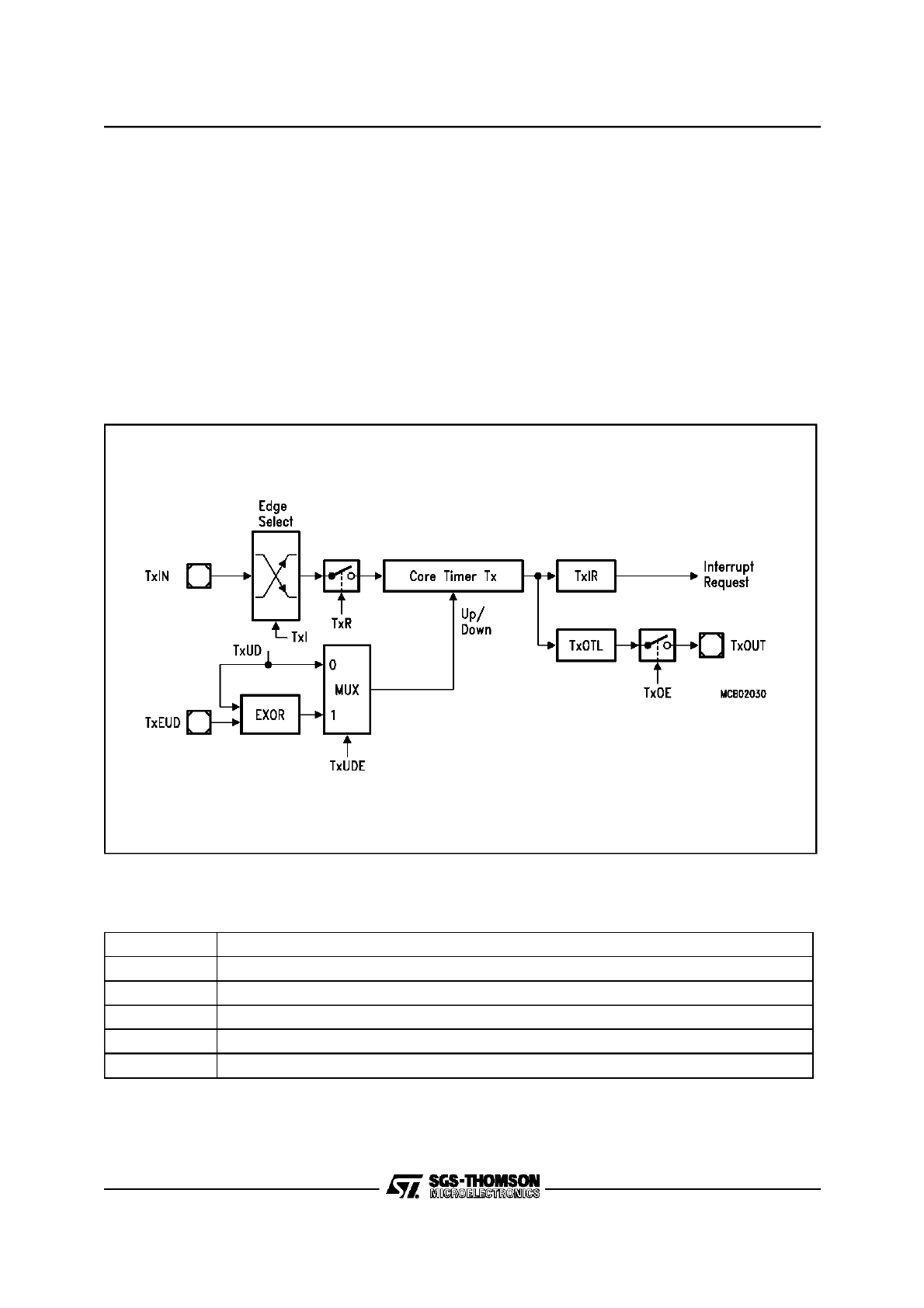
21/28
8 - GENERAL PURPOSE TIMER UNITS (ST10R163)
TIMER BLOCK GPT1 (Cont’d)
Timer 6 in Counter Mode
Counter mode for the core timer T6 is selected by
setting bit field T6M in register T6CON to ‘001b’. In
counter mode timer T6 is clocked by a transition at
the external input pin T6IN, which is an alternate
function of P5.12. The event causing an increment
or decrement of the timer can be a positive, a neg-
ative, or both a positive and a negative transition
at this pin. Bit field T6I in control register T6CON
selects the triggering transition (see table below).
The maximum input frequency which is allowed in
counter mode is f
CPU
/4 (2.5 MHz @ f
CPU
=20 MHz).
To ensure that a transition of the count input signal
which is applied to T6IN is correctly recognized, its
level should be held high or low for at least 4 f
CPU
cycles before it changes.
Figure 5-15. Block Diagram of Core Timer T6 in Counter Mode
GPT2 Core Timer T6 (Counter Mode) Input Edge Selection
T6IN
=
P5.12
T6EUD
=
P5.10
T6OUT
=
P3.1
x = 6
T6I
Trigg ering Edge for Count er Increment / Decrement
0 0 0
None. Counter T6 is disabled
0 0 1
Positive transition (rising edge) on T6IN
0 1 0
Negative transition (falling edge) on T6IN
0 1 1
Any transition (rising or falling edge) on T6IN
1 X X
Reserved. Do not use this combination
151
22/28
8 - GENERAL PURPOSE TIMER UNITS (ST10R163)
TIMER BLOCK GPT1 (Cont’d)
8.2.2 GPT2 Auxiliary Timer T5
The auxiliary timer T5 can be configured for timer,
gated timer, or counter mode with the same op-
tions for the timer frequencies and the count signal
as the core timer T6. In addition to these 3 count-
ing modes, the auxiliary timer can be concatenat-
ed with the core timer.
Note: The auxiliary timer has no output toggle
latch and no alternate output function.
The individual configuration for timer T5 is deter-
mined by its bitaddressable
control register
T5CON. Note that functions which are present in
both timers of block GPT2 are controlled in the
same bit positions and in the same manner in
each of the specific control registers.
T5CON (FF46h / A3h)
SFR
Reset Value: 0000h
*)
For the effects of bits TxUD and TxUDE refer to the direction table (see T6 section).
Bit
Function
T5I
Timer 5 Input Selection
Depends on the Operating Mode, see respective sections.
T5M
Timer 5 Mode Control (Basic Operating Mode)
0 0 :
Timer Mode
0 1 :
Counter Mode
1 0 :
Gated Timer with Gate active low
1 1 :
Gated Timer with Gate active high
T5R
Timer 5 Run Bit
T5R = ‘0’:
Timer / Counter 5 stops
T5R = ‘1’:
Timer / Counter 5 runs
T5UD
Timer 5 Up / Down Control
*)
T5UDE
Timer 5 External Up/Down Enable
*)
CI
Register CAPREL Inpu t Selection
0 0 :
Capture disabled
0 1 :
Positive transition (rising edge) on CAPIN
1 0 :
Negative transition (falling edge) on CAPIN
1 1 :
Any transition (rising or falling edge) on CAPIN
T5CLR
Timer 5 Clear Bit
T5CLR = ‘0’:
Timer 5 not cleared on a capture
T5CLR = ‘1’:
Timer 5 is cleared on a capture
T5SC
Timer 5 Capture Mode Enable
T5SC = ‘0’:
Capture into register CAPREL Disabled
T5SC = ‘1’:
Capture into register CAPREL Enabled
5
4
3
2
1
0
11
10
9
8
7
6
15
14
13
12
-
rw
rw
-
-
-
rw
rw
rw
rw
rw
rw
T5I
-
T5R
T5UD
-
T5
UDE
T5M
T5
CLR
CI
-
-
T5SC
152
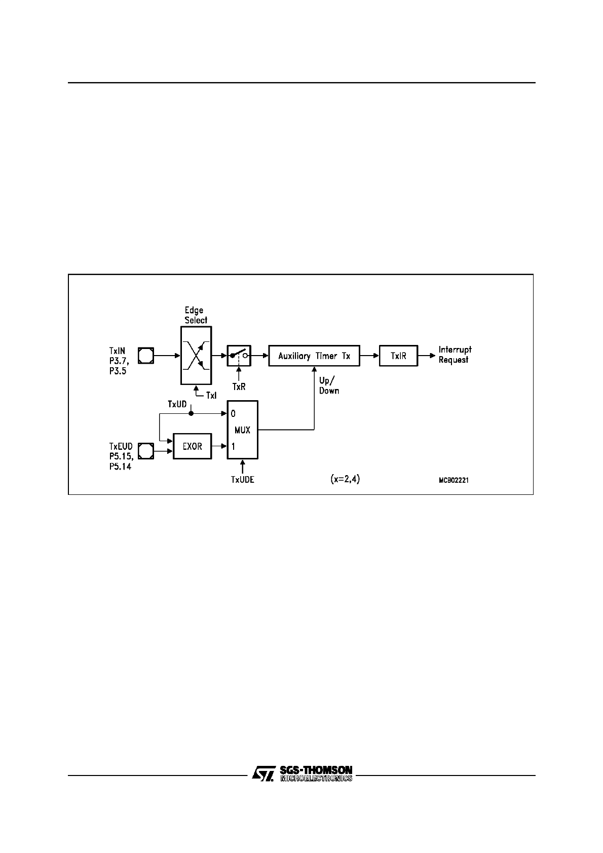
23/28
8 - GENERAL PURPOSE TIMER UNITS (ST10R163)
TIMER BLOCK GPT1 (Cont’d)
Count Direction Control for Auxiliary Timer
The count direction of the auxiliary timer can be
controlled in the same way as for the core timer
T6. The description and the table apply according-
ly.
Timer T5 in Timer Mode or Gated Timer Mode
When the auxiliary timer T5 is programmed to tim-
er mode or gated timer mode, its operation is the
same as described for the core timer T6. The de-
scriptions, figures and tables apply accordingly
with one exception:
•
There is no output toggle latch and no alternate
output pin for T5.
Timer T5 in Counter Mode
Counter mode for the auxiliary timer T5 is selected
by setting bit field T5M in register T5CON to
‘001b’. In counter mode timer T5 can be clocked
either by a transition at the external input pin T5IN,
or by a transition of timer T6’s output toggle latch
T6OTL.
Figure 5-16. Block Diagram of Auxiliary Timer T5 in Counter Mode
The event causing an increment or decrement of
the timer can be a positive, a negative, or both a
positive and a negative transition at either the in-
put pin, or at the toggle latch T6OTL.
Bit field T5I in control register T5CON selects the
triggering transition (see table below).
Note: Only state transitions of T6OTL which are
caused by the overflows/underflows of T6 will trig-
ger the counter function of T5. Modifications of
T6OTL via software will NOT trigger the counter
function of T5.
The maximum input frequency which is allowed in
counter mode is f
CPU
/4 (2.5 MHz @ f
CPU
=20 MHz).
To ensure that a transition of the count input signal
which is applied to T5IN is correctly recognized, its
level should be held high or low for at least 4 f
CPU
cycles before it changes.
x = 5
153
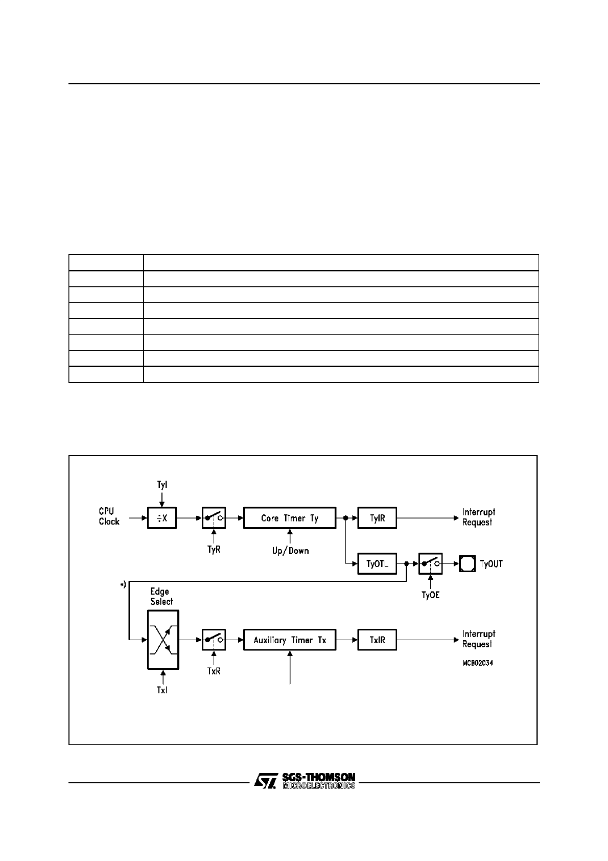
24/28
8 - GENERAL PURPOSE TIMER UNITS (ST10R163)
TIMER BLOCK GPT1 (Cont’d)
Timer Concatenation
Using the toggle bit T6OTL as a clock source for
the auxiliary timer in counter mode concatenates
the core timer T6 with the auxiliary timer. Depend-
ing on which transition of T6OTL is selected to
clock the auxiliary timer, this concatenation forms
a 32-bit or a 33-bit timer / counter.
•
32-bit Timer/Counter: If both a positive and a
negative transition of T6OTL is used to clock the
auxiliary timer, this timer is clocked on every over-
flow/underflow of the core timer T6. Thus, the two
timers form a 32-bit timer.
•
33-bit Timer/Counter: If either a positive or a
negative transition of T6OTL is selected to clock
the auxiliary timer, this timer is clocked on every
second overflow/underflow of the core timer T6.
This configuration forms a 33-bit timer (16-bit core
timer+T6OTL+16-bit auxiliary timer).
GPT2 Auxiliary Timer (Counter Mode) Input Edge Selection
The count directions of the two concatenated tim-
ers are not required to be the same. This offers a
wide variety of different configurations.
T6 can operate in timer, gated timer or counter
mode in this case.
Figure 5-17. Concatenation of Core Timer T6 and Auxiliary Timer T5
T5I
Triggering Edge for Counter Increment / Decrement
X 0 0
None. Counter T5 is disabled
0 0 1
Positive transition (rising edge) on T5IN
0 1 0
Negative transition (falling edge) on T5IN
0 1 1
Any transition (rising or falling edge) on T5IN
1 0 1
Positive transition (rising edge) of output toggle latch T6OTL
1 1 0
Negative transition (falling edge) of output toggle latch T6OTL
1 1 1
Any transition (rising or falling edge) of output toggle latch T6OTL
*)
Note: Line only affected by over/underflows of T6, but NOT by software modifications of T6OTL.
T6OUT
=
P3.1
x =5 y = 6
154
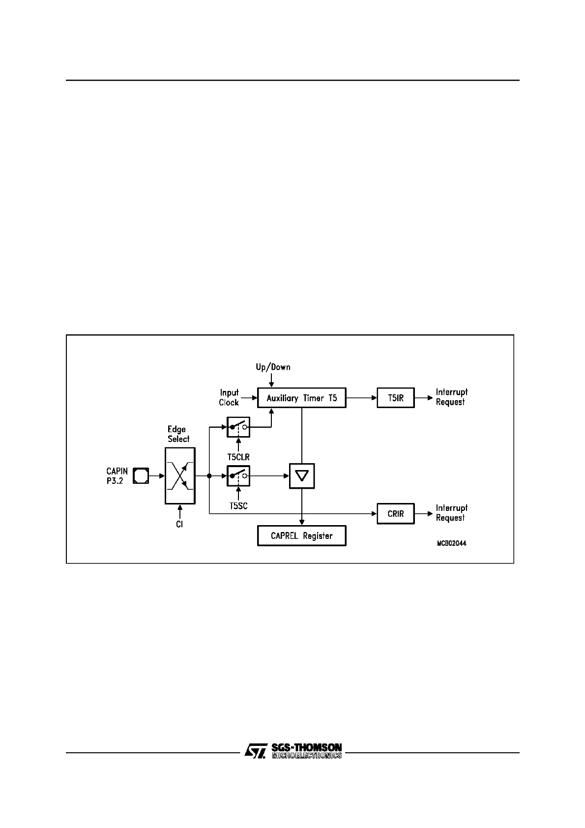
25/28
8 - GENERAL PURPOSE TIMER UNITS (ST10R163)
TIMER BLOCK GPT1 (Cont’d)
GPT2 Capture/Reload Register CAPREL in
Capture Mode
This 16-bit register can be used as a capture reg-
ister for the auxiliary timer T5. This mode is select-
ed by setting bit T5SC=‘1’ in control register
T5CON. The source for a capture trigger is the ex-
ternal input pin CAPIN, which is an alternate input
function of port pin P3.2. Either a positive, a nega-
tive, or both a positive and a negative transition at
this pin can be selected to trigger the capture func-
tion. The active edge is controlled by bit field CI in
register T5CON. The same coding is used as in
the two least significant bits of bit field T5I (see ta-
ble in counter mode section).
The maximum input frequency for the capture trig-
ger signal at CAPIN is f
CPU
/4 (2.5 MHz @ f
CPU
=20
MHz). To ensure that a transition of the capture
trigger signal is correctly recognized, its level
should be held for at least 4 f
CPU
cycles before it
changes.
When a selected transition at the external input
pin CAPIN is detected, the contents of the auxilia-
ry timer T5 are latched into register CAPREL, and
interrupt request flag CRIR is set. With the same
event, timer T5 can be cleared to 0000H. This op-
tion is controlled by bit T5CLR in register T5CON.
If T5CLR=‘0’, the contents of timer T5 are not af-
fected by a capture. If T5CLR=‘1’, timer T5 is
cleared after the current timer value has been
latched into register CAPREL.
Bit T5SC only controls whether a capture is per-
formed or not. If T5SC=‘0’, the input pin CAPIN
can still be used to clear timer T5 or as an external
interrupt input. This interrupt is controlled by the
CAPREL interrupt control register CRIC.
Figure 5-18. GPT2 Register CAPREL in Capture Mode
155
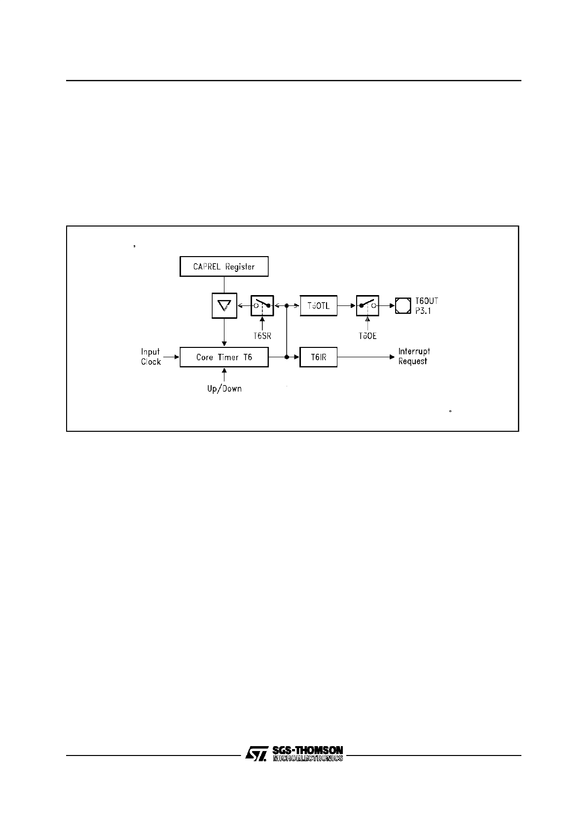
26/28
8 - GENERAL PURPOSE TIMER UNITS (ST10R163)
TIMER BLOCK GPT1 (Cont’d)
GPT2 Capture/Reload Register CAPREL in Re-
load Mode
This 16-bit register can be used as a reload regis-
ter for the core timer T6. This mode is selected by
setting bit T6SR=‘1’ in register T6CON. The event
causing a reload in this mode is an overflow or un-
derflow of the core timer T6.
When timer T6 overflows from FFFFh to 0000h
(when counting up) or when it underflows from
0000h to FFFFh (when counting down), the value
stored in register CAPREL is loaded into timer T6.
This will not set the interrupt request flag CRIR as-
sociated with the CAPREL register. However, in-
terrupt request flag T6IR will be set indicating the
overflow/underflow of T6.
Figure 5-19. GPT2 Register CAPREL in Reload Mode
VR02045H
156
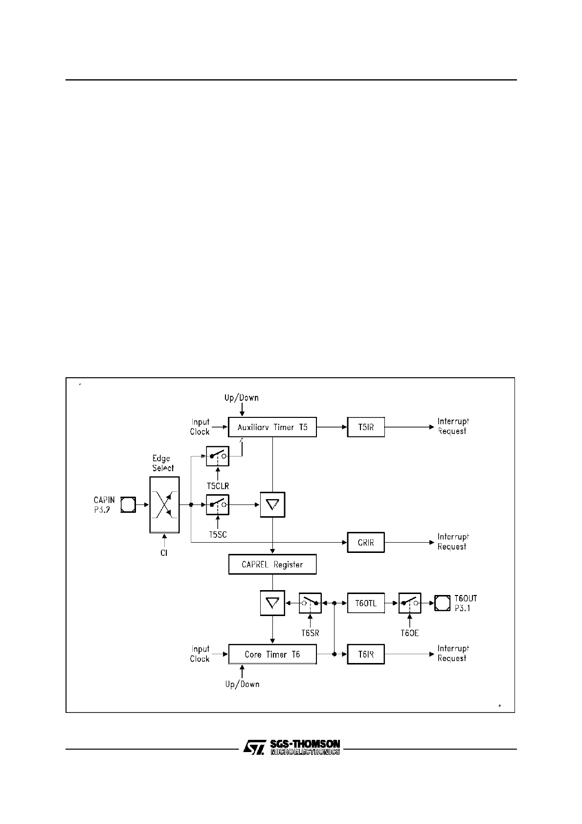
27/28
8 - GENERAL PURPOSE TIMER UNITS (ST10R163)
TIMER BLOCK GPT1 (Cont’d)
GPT2 Capture/Reload Register CAPREL in
Capture-And-Reload Mode
Since the reload function and the capture function
of register CAPREL can be enabled individually by
bits T5SC and T6SR, the two functions can be en-
abled simultaneously by setting both bits. This
feature can be used to generate an output fre-
quency that is a multiple of the input frequency.
This combined mode can be used to detect con-
secutive external events which may occur aperi-
odically, but where a finer resolution, that means,
more ’ticks’ within the time between two external
events is required.
For this purpose, the time between the external
events is measured using timer T5 and the
CAPREL register. Timer T5 runs in timer mode
counting up with a frequency of eg. f
CPU
/32. The
external events are applied to pin CAPIN. When
an external event occurs, the timer T5 contents
are latched into register CAPREL, and timer T5 is
cleared (T5CLR=‘1’). Thus, register CAPREL al-
ways contains the correct time between two
events, measured in timer T5 increments. Timer
T6, which runs in timer mode counting down with a
frequency of eg. f
CPU
/4, uses the value in register
CAPREL to perform a reload on underflow. This
means, the value in register CAPREL represents
the time between two underflows of timer T6, now
measured in timer T6 increments. Since timer T6
runs 8 times faster than timer T5, it will underflow
8 times within the time between two external
events. Thus, the underflow signal of timer T6
generates 8 ’ticks’. Upon each underflow, the in-
terrupt request flag T6IR will be set and bit T6OTL
will be toggled. The state of T6OTL may be output
on pin T6OUT. This signal has 8 times more tran-
sitions than the signal which is applied to pin CAP-
IN.
Figure 5-20. GPT2 Register CAPREL in Capture-And-Reload Mode
VR02045G
157
28/28
8 - GENERAL PURPOSE TIMER UNITS (ST10R163)
TIMER BLOCK GPT1 (Cont’d)
8.2.3 Interrupt Control for GPT2 Timers and
CAPREL
When a timer overflows from FFFFh to 0000h
(when counting up), or when it underflows from
0000h to FFFFh (when counting down), its inter-
rupt request flag (T5IR or T6IR) in register TxIC
will be set. Whenever a transition according to the
selection in bit field CI is detected at pin CAPIN,
interrupt request flag CRIR in register CRIC is set.
Setting any request flag will cause an interrupt to
the respective timer or CAPREL interrupt vector
(T5INT, T6INT or CRINT) or trigger a PEC serv-
ice, if the respective interrupt enable bit (T5IE or
T6IE in register TxIC, CRIE in register CRIC) is
set. There is an interrupt control register for each
of the two timers and for the CAPREL register.
T5IC (FF66h / B3h)
SFR
Reset Value: - - 00h
T6IC (FF68h / B4h)
SFR
Reset Value: - - 00h
CRIC (FF6Ah / B5h)
SFR
Reset Value: - - 00h
Note: Please refer to the general Interrupt Control Register description for an explanation of the control fields.
5
4
3
2
1
0
11
10
9
8
7
6
15
14
13
12
rw
rw
-
-
-
-
rw
rw
-
-
-
-
T5IE
T5IR
GLVL
ILVL
5
4
3
2
1
0
11
10
9
8
7
6
15
14
13
12
rw
rw
-
-
-
-
rw
rw
-
-
-
-
T6IE
T6IR
GLVL
ILVL
5
4
3
2
1
0
11
10
9
8
7
6
15
14
13
12
rw
rw
-
-
-
-
rw
rw
-
-
-
-
CRIE
CRIR
GLVL
ILVL
158

February 1996
1/12
This is advance information from SGS-TH OMSON. Details are subject tochange without notice.
ST10R163
User Manual
9 - ASYNCHRONOUS/SYNCHRONOUS SERIAL INTERFACE
The Asynchronous/Synchronous Serial Interface
ASC0 provides serial communication between the
ST10R163 and other microcontrollers, microproc-
essors or external peripherals.
The ASC0 supports full-duplex asynchronous
communication up to 625 KBaud and half-duplex
synchronous communication up to 2.5 MBaud (@
20 MHz CPU clock). In synchronous mode, data
are transmitted or received synchronous to a shift
clock which is generated by the ST10R163. In
asynchronous mode, 8- or 9-bit data transfer, pari-
ty generation, and the number of stop bits can be
selected. Parity, framing, and overrun error detec-
tion is provided to increase the reliability of data
transfers. Transmission and reception of data is
double-buffered. For multiprocessor communica-
tion, a mechanism to distinguish address from
data bytes is included. Testing is supported by a
loop-back option. A 13-bit baud rate generator
provides the ASC0 with a separate serial clock
signal.
The operating mode of the serial channel ASC0 is
controlled by its bitaddressable control register
S0CON. This register contains control bits for
mode and error check selection, and status flags
for error identification.
A transmission is started by writing to the (write-
only) Transmit Buffer register S0TBUF (via an in-
struction or a PEC data transfer). Only the number
of data bits which is determined by the selected
operating mode will actually be transmitted, ie. bits
written to positions 9 through 15 of register
S0TBUF are always insignificant. After a transmis-
sion has been completed, the transmit buffer reg-
ister is cleared to 0000h.
Data transmission is double-buffered, so a new
character may be written to the transmit buffer
register, before the transmission of the previous
character is complete. This allows to send charac-
ters back-to-back without gaps.
Data reception is enabled by the Receiver Enable
Bit S0REN. After reception of a character has
been completed, the received data and, if provid-
ed by the selected operating mode, the received
parity bit can be read from the (read-only) Receive
Buffer register S0RBUF. Bits in the upper half of
S0RBUF which are not valid in the selected oper-
ating mode will be read as zeros.
Data reception is double-buffered, so that recep-
tion of a second character may already begin be-
fore the previously received character has been
read out of the receive buffer register. In all
modes, receive buffer overrun error detection can
be selected through bit S0OEN. When enabled,
the overrun error status flag S0OE and the error
interrupt request flag S0EIR will be set when the
receive buffer register has not been read by the
time reception of a second character is complete.
The previously received character in the receive
buffer is overwritten.
The Loop-Back option (selected by bit S0LB) al-
lows to simultaneously receive the data currently
being transmitted. This may be used to test serial
communication routines at an early stage without
having to provide an external network. In loop-
back mode the alternate input/output functions of
the Port 3 pins are not necessary.
Note: Serial data transmission or reception is only
possible when the Baud Rate Generator Run Bit
S0R is set to ‘1’. Otherwise the serial interface is
idle.
Do not program the mode control field S0M in reg-
ister S0CON to one of the reserved combinations
to avoid unpredictable behaviour of the serial in-
terface.
S0CON (FFB0h / D8h)
SFR
Reset Value: 0000h
S0FE
5
4
3
2
1
0
11
10
9
8
7
6
15
14
13
12
rw
rw
rw
rw
-
rw
rw
rw
rw
rw
rw
rw
-
S0LB
S0R
S0PE
S0
STP
S0
REN
S0
PEN
S0
FEN
S0
OEN
rw
rw
S0OE
S0
ODD
S0
BRS
S0M
159

2/12
9 - ASYNCHRONOUS/SYNCHRONOUS SERIAL INTERFACE (ST10R163)
Table 1. SFRs and Port Pins associated with ASC0
Bit
Functio n
S0M
ASC0 Mode Control
0 0 0 :
8-bit data
synchronous operation
0 0 1 :
8-bit data
async. operation
0 1 0 :
Reserved. Do not use this combination!
0 1 1 :
7-bit data + parity
async. operation
1 0 0 :
9-bit data
async. operation
1 0 1 :
8-bit data + wake up bit
async. operation
1 1 0 :
Reserved. Do not use this combination!
1 1 1 :
8-bit data + parity
async. operation
S0STP
Number of Stop Bits Selection
async. operation
0 :
One stop bit
1 :
Two stop bits
S0REN
Receiver Enable Bit
0 :
Receiver disabled
1 :
Receiver enabled
(Reset by hardware after reception of byte in synchronous mode)
S0PEN
Parity Check Enable Bit
async. operation
0 :
Ignore parity
1 :
Check parity
S0FEN
Framing Check Enable Bit
async. operation
0 :
Ignore framing errors
1 :
Check framing errors
S0OEN
Overrun Check Enable Bit
0 :
Ignore overrun errors
1 :
Check overrun errors
S0PE
Parity Error Flag
Set by hardware on a parity error (S0PEN=’1’). Must be reset by software.
S0FE
Framing Error Flag
Set by hardware on a framing error (S0FEN=’1’). Must be reset by software.
S0OE
Overrun Error Flag
Set by hardware on an overrun error (S0OEN=’1’). Must be reset by software.
S0ODD
Parity Selection Bit
0 :
Even parity (parity bit set on odd number of ‘1’s in data)
1 :
Odd parity (parity bit set on even number of ‘1’s in data)
S0BRS
Baudrate Selection Bit
0 :
Divide clock by reload-value + constant (depending on mode)
1 :
Additionally reduce serial clock to 2/3rd
S0LB
LoopBack Mode Enable Bit
0 :
Standard transmit/receive mode
1 :
Loopback mode enabled
S0R
Baudrate Generator Run Bit
0 :
Baudrate generator disabled (ASC0 inactive)
1 :
Baudrate generator enabled
160
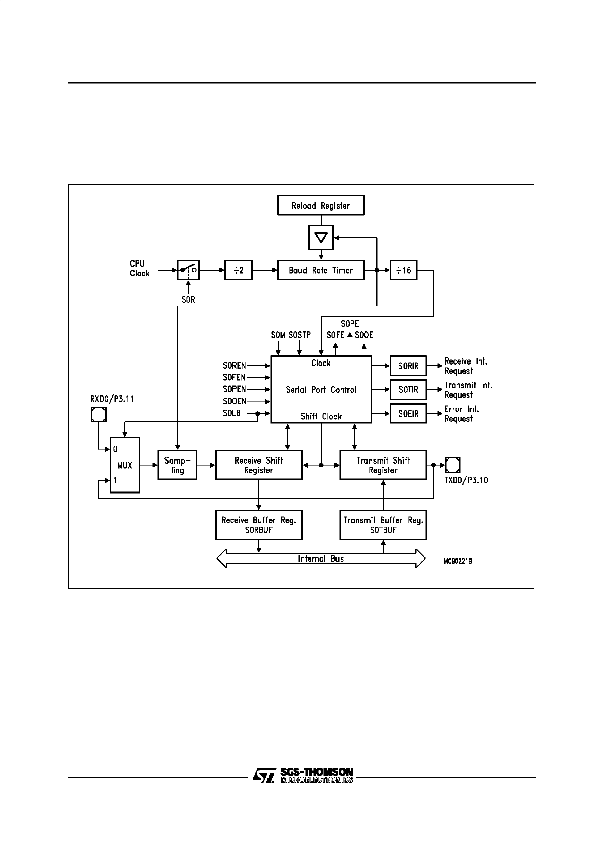
3/12
9 - ASYNCHRONOUS/SYNCHRONOUS SERIAL INTERFACE (ST10R163)
9.1 ASYNCHRONOUS OPERATION
Asynchronous mode supports full-duplex commu-
nication, where both transmitter and receiver use
the same data frame format and the same baud
rate. Data is transmitted on pin TXD0/P3.10 and
received on pin RXD0/P3.11. These signals are
alternate functions of Port 3 pins.
Figure 6-1. Asynchronous Mode of Serial Channel ASC0
161
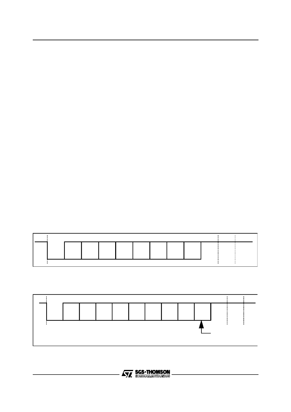
4/12
9 - ASYNCHRONOUS/SYNCHRONOUS SERIAL INTERFACE (ST10R163)
ASYNCHRONOUS OPERATION(Cont’d)
Asynchronous Data Frames
8-bit data frames either consist of 8 data bits
D7...D0 (S0M=’001b’), or of 7 data bits D6...D0
plus
an
automatically
generated
parity
bit
(S0M=’011b’). Parity may be odd or even, de-
pending on bit S0ODD in register S0CON. An
even parity bit will be set, if the modulo-2-sum of
the 7 data bits is ‘1’. An odd parity bit will be
cleared in this case. Parity checking is enabled via
bit S0PEN (always OFF in 8-bit data mode). The
parity error flag S0PE will be set along with the er-
ror interrupt request flag, if a wrong parity bit is re-
ceived. The parity bit itself will be stored in bit
S0RBUF.7.
9-bit data frames either consist of 9 data bits
D8...D0 (S0M=’100b’), of 8 data bits D7...D0 plus
an
automatically
generated
parity
bit
(S0M=’111b’) or of 8 data bits D7...D0 plus wake-
up bit (S0M=’101b’). Parity may be odd or even,
depending on bit S0ODD in register S0CON. An
even parity bit will be set, if the modulo-2-sum of
the 8 data bits is ‘1’. An odd parity bit will be
cleared in this case. Parity checking is enabled via
bit S0PEN (always OFF in 9-bit data and wake-up
mode). The parity error flag S0PE will be set along
with the error interrupt request flag, if a wrong par-
ity bit is received. The parity bit itself will be stored
in bit S0RBUF.8.
In wake-up mode received frames are only trans-
ferred to the receive buffer register, if the 9th bit
(the wake-up bit) is ‘1’. If this bit is ‘0’, no receive
interrupt request will be activated and no data will
be transferred.
This feature may be used to control communica-
tion in multi-processor system:
When the master processor wants to transmit a
block of data to one of several slaves, it first sends
out an address byte which identifies the target
slave. An address byte differs from a data byte in
that the additional 9th bit is a ’1’ for an address
byte and a ’0’ for a data byte, so no slave will be in-
terrupted by a data ’byte’. An address ’byte’ will in-
terrupt all slaves (operating in 8-bit data + wake-
up bit mode), so each slave can examine the 8
LSBs of the received character (the address). The
addressed slave will switch to 9-bit data mode (eg.
by clearing bit S0M.0), which enables it to also re-
ceive the data bytes that will be coming (having
the wake-up bit cleared). The slaves that were not
being addressed remain in 8-bit data + wake-up
bit mode, ignoring the following data bytes.
Figure 6-2. Asynchronous 8-bit Data Frames
Figure 6-3. Asynchronous 9-bit Data Frames
2nd
Stop
Bit
Start
Bit
D0
(LSB)
D1
D2
D3
D4
D5
D6
D7 /
Parity
(1st)
Stop
Bit
2nd
Stop
Bit
Start
Bit
D0
(LSB)
D1
D2
D3
D4
D5
D6
9th
Bit
(1st)
Stop
Bit
D7
•
Data Bit D8
•
Parity
•
Wake-up Bit
162

5/12
9 - ASYNCHRONOUS/SYNCHRONOUS SERIAL INTERFACE (ST10R163)
ASYNCHRONOUS OPERATION(Cont’d)
Asynchronous transmission begins at the next
overflow of the divide-by-16 counter (see figure
above), provided that S0R is set and data has
been loaded into S0TBUF. The transmitted data
frame consists of three basic elements:
– the start bit
– the data field (8 or 9 bits, LSB first, including a
parity bit, if selected)
– the delimiter (1 or 2 stop bits)
Data transmission is double buffered. When the
transmitter is idle, the transmit data loaded into
S0TBUF is immediately moved to the transmit
shift register thus freeing S0TBUF for the next
data to be sent. This is indicated by the transmit
buffer interrupt request flag S0TBIR being set.
S0TBUF may now be loaded with the next data,
while transmission of the previous one is still going
on.
The transmit interrupt request flag S0TIR will be
set before the last bit of a frame is transmitted, ie.
before the first or the second stop bit is shifted out
of the transmit shift register.
The transmitter output pin TXD0/P3.10 must be
configured for alternate data output, ie. P3.10=’1’
and DP3.10=’1’.
Asynchronous reception is initiated by a falling
edge (1-to-0 transition) on pin RXD0, provided
that bits S0R and S0REN are set. The receive
data input pin RXD0 is sampled at 16 times the
rate of the selected baud rate. A majority decision
of the 7th, 8th and 9th sample determines the ef-
fective bit value. This avoids erroneous results
that may be caused by noise.
If the detected value is not a ’0’ when the start bit is
sampled, the receive circuit is reset and waits for
the next 1-to-0 transition at pin RXD0. If the start
bit proves valid, the receive circuit continues sam-
pling and shifts the incoming data frame into the
receive shift register.
When the last stop bit has been received, the con-
tent of the receive shift register is transferred to
the receive data buffer register S0RBUF. Simulta-
neously, the receive interrupt request flag S0RIR
is set after the 9th sample in the last stop bit time
slot (as programmed), regardless whether valid
stop bits have been received or not. The receive
circuit then waits for the next start bit (1-to-0 tran-
sition) at the receive data input pin.
The receiver input pin RXD0/P3.11 must be con-
figured for input, ie. DP3.11=’0’.
Asynchronous reception is stopped by clearing bit
S0REN. A currently received frame is completed
including the generation of the receive interrupt re-
quest and an error interrupt request, if appropri-
ate. Start bits that follow this frame will not be rec-
ognized.
Note: In wake-up mode received frames are only
transferred to the receive buffer register, if the 9th
bit (the wake-up bit) is ‘1’. If this bit is ‘0’, no re-
ceive interrupt request will be activated and no
data will be transferred.
163
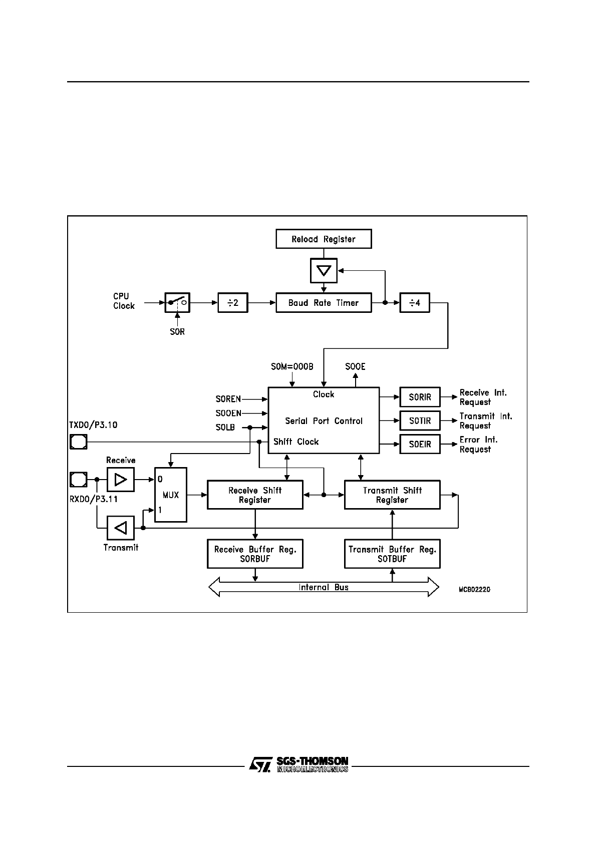
6/12
9 - ASYNCHRONOUS/SYNCHRONOUS SERIAL INTERFACE (ST10R163)
9.2 SYNCHRONOUS OPERATION
Synchronous mode supports half-duplex commu-
nication, basically for simple IO expansion via shift
registers. Data is transmitted and received via pin
RXD0/P3.11, while pin TXD0/P3.10 outputs the
shift clock. These signals are alternate functions
of Port 3 pins. Synchronous mode is selected with
S0M=’000b’.
8 data bits are transmitted or received synchro-
nous to a shift clock generated by the internal
baud rate generator. The shift clock is only active
as long as data bits are transmitted or received.
Figure 6-4. Synchronous Mode of Serial Channel ASC0
164

7/12
9 - ASYNCHRONOUS/SYNCHRONOUS SERIAL INTERFACE (ST10R163)
SYNCHRONOUS OPERATION (Cont’d)
Synchronous transmissionbegins within 4 state
times after data has been loaded into S0TBUF,
provided that S0R is set and S0REN=’0’ (half-du-
plex, no reception). Data transmission is double
buffered. When the transmitter is idle, the transmit
data loaded into S0TBUF is immediately moved to
the transmit shift register thus freeing S0TBUF for
the next data to be sent. This is indicated by the
transmit buffer interrupt request flag S0TBIR be-
ing set. S0TBUF may now be loaded with the next
data, while transmission of the previous one is still
going on. The data bits are transmitted synchro-
nous with the shift clock. After the bit time for the
8th data bit, both pins TXD0 and RXD0 will go
high, the transmit interrupt request flag S0TIR is
set, and serial data transmission stops.
Pin TXD0/P3.10 must be configured for alternate
data output, ie. P3.10=’1’ and DP3.10=’1’, in order
to provide the shift clock. Pin RXD0/P3.11 must
also be configured for output (P3.11=’1’ and
DP3.11=’1’) during transmission.
Synchronous reception is initiated by setting bit
S0REN=’1’. If bit S0R=1, the data applied at pin
RXD0 are clocked into the receive shift register
synchronous to the clock which is output at pin
TXD0. After the 8th bit has been shifted in, the
content of the receive shift register is transferred
to the receive data buffer S0RBUF, the receive in-
terrupt request flag S0RIR is set, the receiver en-
able bit S0REN is reset, and serial data reception
stops.
Pin TXD0/P3.10 must be configured for alternate
data output, ie. P3.10=’1’ and DP3.10=’1’, in order
to provide the shift clock. Pin RXD0/P3.11 must be
configured as alternate data input (DP3.11=’0’).
Synchronous reception is stopped by clearing bit
S0REN. A currently received byte is completed in-
cluding the generation of the receive interrupt re-
quest and an error interrupt request, if appropri-
ate. Writing to the transmit buffer register while a
reception is in progress has no effect on reception
and will not start a transmission.
If a previously received byte has not been read out
of the receive buffer register at the time the recep-
tion of the next byte is complete, both the error in-
terrupt request flag S0EIR and the overrun error
status flag S0OE will be set, provided the overrun
check has been enabled by bit S0OEN.
9.3
HARDWARE
ERROR
DETECTION
CAPABILITIES
To improve the safety of serial data exchange, the
serial channel ASC0 provides an error interrupt re-
quest flag, which indicates the presence of an er-
ror, and three (selectable) error status flags in reg-
ister S0CON, which indicate which error has been
detected during reception. Upon completion of a
reception, the error interrupt request flag S0EIR
will be set simultaneously with the receive inter-
rupt request flag S0RIR, if one or more of the fol-
lowing conditions are met:
•
If the framing error detection enable bit S0FEN
is set and any of the expected stop bits is not
high, the framing error flag S0FE is set, indicat-
ing that the error interrupt request is due to a
framing error (Asynchronous mode only).
•
If the parity error detection enable bit S0PEN is
set in the modes where a parity bit is received,
and the parity check on the received data bits
proves false, the parity error flag S0PE is set,
indicating that the error interrupt request is due
to a parity error (Asynchronous mode only).
•
If the overrun error detection enable bit S0OEN
is set and the last character received was not
read out of the receive buffer by software or
PEC transfer at the time the reception of a new
frame is complete, the overrun error flag S0OE
is set indicating that the error interrupt request
is due to an overrun error (Asynchronous and
synchronous mode).
165

8/12
9 - ASYNCHRONOUS/SYNCHRONOUS SERIAL INTERFACE (ST10R163)
9.4 ASC0 BAUD RATE GENERATION
The serial channel ASC0 has its own dedicated
13-bit baud rate generator with 13-bit reload capa-
bility, allowing baud rate generation independent
from the timers.
The baud rate generator is clocked with the CPU
clock divided by 2 (10 MHz @ 20 MHz CPU clock).
The timer is counting downwards and can be start-
ed or stopped through the Baud Rate Generator
Run Bit S0R in register S0CON. Each underflow
of the timer provides one clock pulse to the serial
channel. The timer is reloaded with the value
stored in its 13-bit reload register each time it un-
derflows. The resulting clock is again divided ac-
cording to the operating mode and controlled by
the Baudrate Selection Bit S0BRS. If S0BRS=’1’,
the clock signal is additionally divided to 2/3rd of
its frequency (see formulas and table). So the
baud rate of ASC0 is determined by the CPU
clock, the reload value, the value of S0BRS and
the operating mode (asynchronous or synchro-
nous).
Register S0BG is the dual-function Baud Rate
Generator/Reload register. Reading S0BG returns
the content of the timer (bits 15...13 return zero),
while writing to S0BG always updates the reload
register (bits 15...13 are insiginificant).
An auto-reload of the timer with the content of the
reload register is performed each time S0BG is
written to. However, if S0R=’0’ at the time the write
operation to S0BG is performed, the timer will not
be reloaded until the first instruction cycle after
S0R=’1’.
Asynchronous Mode Baud Rates
For asynchronous operation, the baud rate gener-
ator provides a clock with 16 times the rate of the
established baud rate. Every received bit is sam-
pled at the 7th, 8th and 9th cycle of this clock. The
baud rate for asynchronous operation of serial
channel ASC0 and the required reload value for a
given baudrate can be determined by the following
formulas:
<S0BRL> represents the content of the reload
register, taken as unsigned 13-bit integer,
<S0BRS> represents the value of bit S0BRS (ie.
‘0’ or ‘1’), taken as integer.
The maximum baud rate that can be achieved for
the asynchronous modes when using a CPU clock
of 20 MHz is 625 KBaud. The table below lists var-
ious commonly used baud rates together with the
required reload values and the deviation errors
compared to the intended baudrate.
B
Async
=
f
CPU
(32 + 16*<S0BRS>) * (<S0BRL> + 1)
S0BRL = (
f
CPU
(32 + 16*<S0BRS>) * B
Async
) - 1
166

9/12
9 - ASYNCHRONOUS/SYNCHRONOUS SERIAL INTERFACE (ST10R163)
ASC0 BAUD RATE GENERATION (Cont’d)
Synchronous Mode Baud Rates
For synchronous operation, the baud rate genera-
tor provides a clock with 4 times the rate of the es-
tablished baud rate. The baud rate for synchro-
nous operation of serial channel ASC0 can be de-
termined by the following formula:
<S0BRL> represents the content of the reload
register, taken as unsigned 13-bit integers,
<S0BRS> represents the value of bit S0BRS (ie.
‘0’ or ‘1’), taken as integer.
The maximum baud rate that can be achieved in
synchronous mode when using a CPU clock of
20 MHz is 2.5 MBaud.
Note: The deviation errors given in the table above are rounded.
Using a baudrate crystal (resulting in a CPU clock of eg. 18.432 MHz) provides correct baudrates without deviation
errors.
B
Sync
=
S0BRL = (
f
CPU
(8 + 4*<S0BRS>) * B
Sync
) - 1
f
CPU
(8 + 4*<S0BRS>) * (<S0BRL> + 1)
Baud Rate
S0BRS = ‘0’, f
CPU
= 20 MHz
S0BRS = ‘1’, f
CPU
= 20 MHz
Deviation Error
Reload Value
Deviation Error
Reload Value
625
KBaud
±
0.0 %
0000h
---
---
19.2
KBaud
+1.7 % / -1.4 %
001Fh / 0020h
+3.3 % / -1.4 %
0014h / 0015h
9600
Baud
+0.2 % / -1.4 %
0040h / 0041h
+1.0 % / -1.4 %
002Ah / 002Bh
4800
Baud
+0.2 % / -0.6 %
0081h / 0082h
+1.0 % / -0.2 %
0055h / 0056h
2400
Baud
+0.2 % / -0.2 %
0103h / 0104h
+0.4 % / -0.2 %
00ACh / 00ADh
1200
Baud
+0.2 % / -0.4 %
0207h / 0208h
+0.1 % / -0.2 %
015Ah / 015Bh
600
Baud
+0.1 % / -0.0 %
0410h / 0411h
+0.1 % / -0.1 %
02B5h / 02B6h
75
Baud
+1.7 %
1FFFh
+0.0 % / -0.0 %
15B2h / 15B3h
167
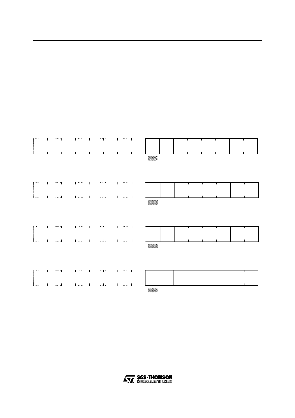
10/12
9 - ASYNCHRONOUS/SYNCHRONOUS SERIAL INTERFACE (ST10R163)
9.5 ASC0 INTERRUPT CONTROL
Four bit addressable interrupt control registers are
provided for serial channel ASC0. Register S0TIC
controls the transmit interrupt, S0TBIC controls
the transmit buffer interrupt, S0RIC controls the
receive interrupt and S0EIC controls the error in-
terrupt of serial channel ASC0. Each interrupt
source also has its own dedicated interrupt vector.
S0TINT is the transmit interrupt vector, S0TBINT
is the transmit interrupt vector, S0RINT is the re-
ceive interrupt vector, and S0EINT is the error in-
terrupt vector.
The cause of an error interrupt request (framing,
parity, overrun error) can be identified by the error
status flags in control register S0CON.
Note: In contrary to the error interrupt request flag
S0EIR, the error status flags S0FE/S0PE/S0OE
are not reset automatically upon entry into the er-
ror interrupt service routine, but must be cleared
by software.
S0TIC (FF6Ch / B6h)
SFR
Reset Value: - - 00h
S0RIC (FF6Eh / B7h)
SFR
Reset Value: - - 00h
S0EIC (FF70h / B8h)
SFR
Reset Value: - - 00h
S0TBIC (F19Ch / CEh)
ESFR
Reset Value: - - 00h
Note: Please refer to the general Interrupt Control Register description for an explanation of the control fields.
5
4
3
2
1
0
11
10
9
8
7
6
15
14
13
12
rw
rw
-
-
-
-
rw
rw
-
-
-
-
S0TIE
S0TIR
GLVL
ILVL
5
4
3
2
1
0
11
10
9
8
7
6
15
14
13
12
rw
rw
-
-
-
-
rw
rw
-
-
-
-
S0RIE
S0RIR
GLVL
ILVL
5
4
3
2
1
0
11
10
9
8
7
6
15
14
13
12
rw
rw
-
-
-
-
rw
rw
-
-
-
-
S0EIE
S0EIR
GLVL
ILVL
S0
TBIR
S0
TBIE
5
4
3
2
1
0
11
10
9
8
7
6
15
14
13
12
rw
rw
-
-
-
-
rw
rw
-
-
-
-
GLVL
ILVL
168
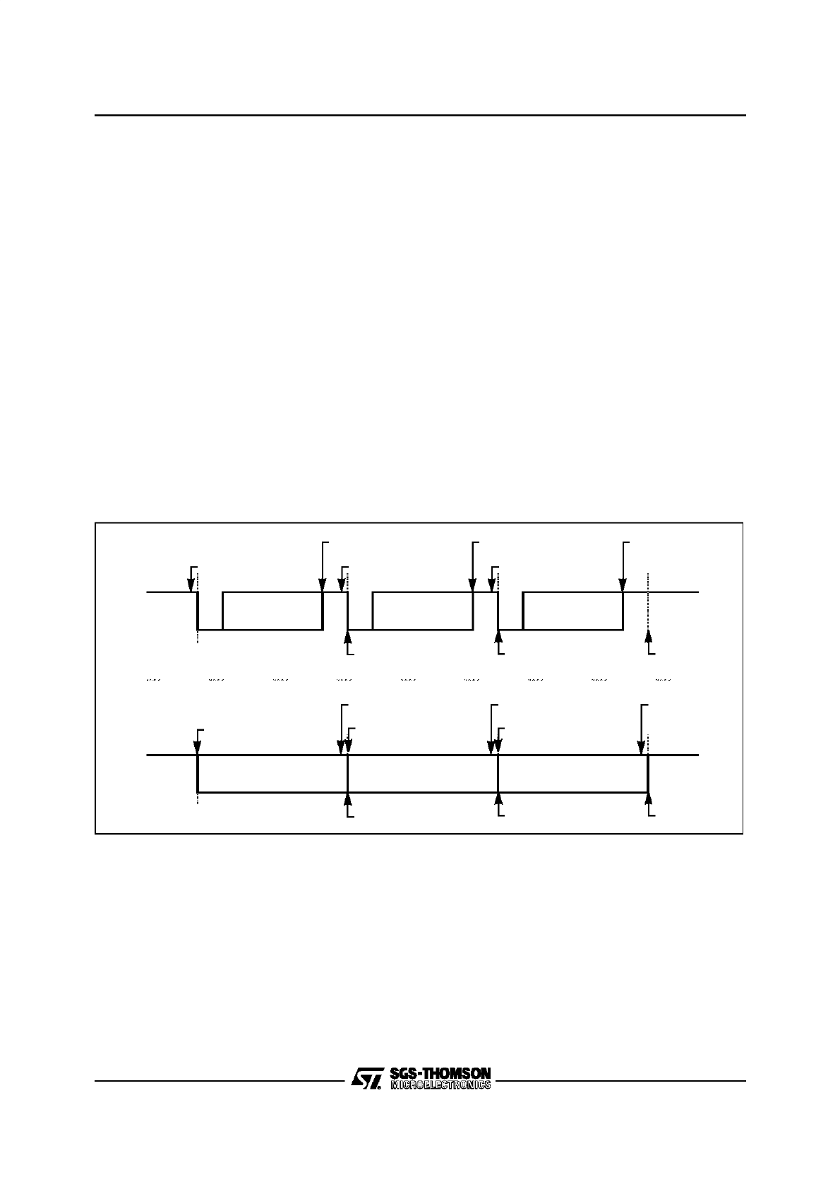
11/12
9 - ASYNCHRONOUS/SYNCHRONOUS SERIAL INTERFACE (ST10R163)
ASC0 INTERRUPT CONTROL(Cont’d)
Using the ASC0 Interrupts
For normal operation (ie. besides the error inter-
rupt) the ASC0 provides three interrupt requests
to control data exchange via this serial channel:
– S0TBIR
is activated when data is moved
from S0TBUF to the transmit shift register.
– S0TIR
is activated before the last bit of an
asynchronous frame is transmitted, or
–
after the last bit of a synchronous
frame has been transmitted.
– S0RIR
is activated when the received
frame is moved to S0RBUF.
While the task of the receive interrupt handler is
quite clear, the transmitter is serviced by two inter-
rupt handlers. This provides advantages for the
servicing software.
For single transfers it is sufficient to use the
transmitter interrupt (S0TIR), which indicates that
the previously loaded data has been transmitted,
except for the last bit of an asynchronous frame.
For multiple back-to-back transfers it is neces-
sary to load the following data at least until the
time the last bit of the previous frame is being
transmitted. In asynchronous mode this leaves
just one bit-time for the handler to respond to the
transmitter
interrupt
request,
in synchronous
mode it is not possible at all.
Using the transmit buffer interrupt (S0TBIR) to re-
load transmit data allows the time to transmit a
complete
frame for the service routine,
as
S0TBUF may be reloaded while the previous data
is still being transmitted.
As shown in the figure below, S0TBIR is an early
trigger for the reload routine, while S0TIR indi-
cates the completed transmission. Software using
handshake therefore should rely on S0TIR at the
end of a data block to make sure that all data has
really been transmitted.
Figure 6-5. ASC0 Interrupt Generation
Idle
Idle
St
ar
t
St
ar
t
St
ar
t
St
op
St
o
p
St
o
p
S0TBIR
S0TBIR
S0TBIR
S0TIR
S0TIR
S0TIR
S0RIR
S0RIR
S0RIR
Idle
Idle
S0TBIR
S0TBIR
S0TBIR
S0TIR
S0TIR
S0TIR
S0RIR
S0RIR
S0RIR
Asynchronous Mode
Synchronous Mode
169

12/12
9 - ASYNCHRONOUS/SYNCHRONOUS SERIAL INTERFACE (ST10R163)
Notes:
170
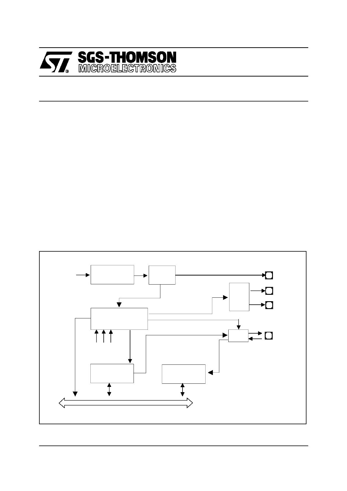
February 1996
1/16
This is advance information from SGS-TH OMSON. Details are subject tochange without notice.
ST10R163
User Manual
10 - SYNCHRONOUS SERIAL PORT
The Synchronous Serial Port SSP provides high-
speed serial communication with external slave
devices such as EEPROM via a three-wire inter-
face similar to the SPI protocol. The interface lines
are:
SSPCLK
Serial clock output. Driven by the
ST10R163 (master) to the peripheral
(slave) which is selected for transfer.
SSPDAT
Bi-directional serial data line. Data is
transferred between the ST10R163
and the peripheral at up to 10 MBit/s.
SSPCE0,1 Serial peripheral chip enable signals 0
and 1. These signals select one of he
slaves connected to the SSP for
transfer.
The SSP can be programmed to send command,
address or data information to a peripheral device
(write operation) or receive data from a peripheral
(read operation). For a write operation, the SSP
can send up to three bytes (24 bits) to a peripher-
al. For a read operation, the SSP can first send up
to three bytes to a peripheral before receiving one
byte from the peripheral. In addition, a continuous
mode is provided which allows to continuously
send data to the selected peripheral or continu-
ously receive data from the selected peripheral,
without deselecting the peripheral between the
single transfers. With this feature, reading for ex-
ample EEPROM devices is simplified such that af-
ter the initial command and address transfer from
the master to the peripheral, data bytes can be
read from the peripheral one after the other.
Figure 7-1. Synchronous Serial Port SSP Block Diagram
VR02079B
Chip
Enable
Control
SSP Control
Block
Status
X BUS
Transmit Buffers
Registers SSPTBx
Receive Buffers
Registers SSPRB
Control
Pin
XP1INT
Clock Rate
Divider
Control
Clock
Clock
Shift
Clock
CPU
Receive/Transmit
Int. Request
SSPLCK
SSPCE0
SSPCE1
SSPDAT
171
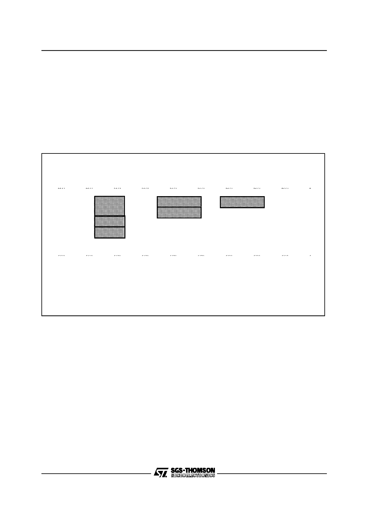
2/16
10 - SYNCHRONOUS SERIAL PORT (ST10R163)
XBUS Implementation
The SSP is implemented as an on-chip X-Periph-
eral connected onto the XBUS. From a user’s
point of view, this XBUS can be regarded as an in-
ternal representation of the external bus in the 16-
bit demultiplexed mode, allowing fastest possible
word and byte accesses by the CPU or the PEC to
the registers of the SSP. These registers reside in
a special SSP address area of 256 bytes, which is
mapped into segment 0 and uses addresses
EF00h through EFFFh (10 bytes addresses used).
SSP Registers
The registers of the SSP are organized as five 16-
bit registers, located on word addresses. Howev-
er, all registers may be accessed bytewise in or-
der to select special actions without effecting other
mechanisms. The figure below shows all control
and data registers of the SSP.
Figure 7-2. Synchronous Serial Port SSP Registers
XP1IC
SSPT B0
SSP Transmit Byte 0 Register
SSPT B1
SSP Transmit Byte 1 Register
SSPT B2
SSP Transmit Byte 2 Register
SSPRB0
SSP Receive Byte 0 Register (same location
than SSPTB0 )
SSPCON0 SSP Control Register 0
SSPCON1 SSP Control Register 1
XP1IC
SSP Interrupt Control Register
Data Registers
(8-bit registers)
Control Registers
Interrupt Control
SSPTB0
SSPCON0
SSPTB1
SSPTB2
SSPRB0
SSPCON1
172

3/16
10 - SYNCHRONOUS SERIAL PORT (ST10R163)
SSP Control Register 0 - SSPCON0
This register contains all bits which are required to
setup a read or write operation for the SSP.
SSPCCON0 (00’EF00h)
Reset Value: 0000h
Bit
Function
SSPCKS
SSP Clock Rate Selection
Baud Rate @ 20 MHz CPU clock
000:
SSP clock = CPU clock divided by 2
10
MBit/s.
001:
SSP clock = CPU clock divided by 4
5
MBit/s.
010:
SSP clock = CPU clock divided by 8
2.5
MBit/s.
011:
SSP clock = CPU clock divided by 16
1.25
MBit/s.
100:
SSP clock = CPU clock divided by 32
625
KBit/s.
101:
SSP clock = CPU clock divided by 64
312.5
KBit/s.
110:
SSP clock = CPU clock divided by 128
156.25
KBit/s.
111:
SSP clock = CPU clock divided by 256
78.125
KBit/s.
SSPSEL
SSP Chip Enable Selection
00:No chip enable line selected.
01:Chip enable line 0 (SSPCE0) selected.
10:Chip enable line 1 (SSPCE1) selected.
11:Both chip enable lines selected. Can be used for broadcast messages. Improper
use for read operations may cause line conflicts among several selected slaves.
SSPCM
SSP Continuous Mode Selection
0:Single Transfer Mode. Chip enable line deactivated after end of transfer.
1:Continuous Mode. Chip enable line remains active between transfers.
SSPHB
SSP Heading Control Bit
0:Transmit/Receive LSB First
1:Transmit/Receive MSB First
SSPRW
SSP Read/Write Control Bit
0:Write Operation selected.
1:Read Operation selected.
SSPCKE
SSP Clock Edge Control Bit
0:Shift transmit data on the leading clock edge, latch on trailing edge.
1:Latch receive data on leading clock edge, shift on trailing edge.
SSPCKP
SSP Clock Polarity Control Bit
0:Idle clock is high, leading clock edge is high-to-low transition.
1:Idle clock is low, leading clock edge is low-to-high transition.
SSPBSY
SSP Busy Flag
0:SSP is idle.
1:SSP is busy.
The Busy flag is set with the first write into one of the transmit buffers. It is automatically cleared
after the last bit has been transferred and selected chip select line is switched inactive.
5
4
3
2
1
0
11
10
9
8
7
6
15
14
13
12
rw
rw
rw
-
rw
rw
rw
-
-
-
-
-
SSP
CM
SSP
HB
-
rw
SSP
CKP
SSP
CKE
SSP
RW
SSPCKS
-
SSP
BSY
-
-
SSPSEL
-
173
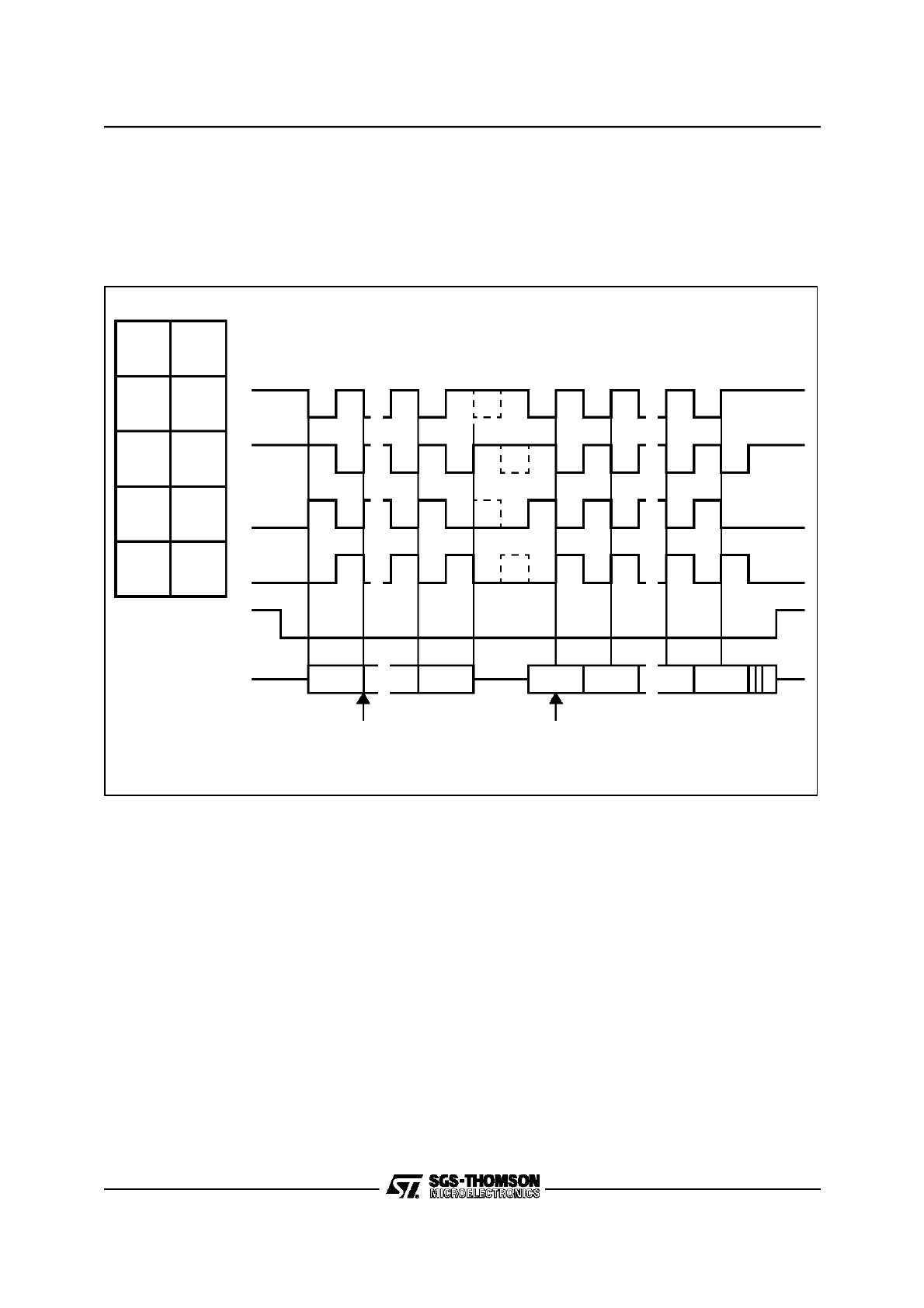
4/16
10 - SYNCHRONOUS SERIAL PORT (ST10R163)
The Clock Control allows to adapt transmit and
receive behaviour of the SSP to a variety of serial
interfaces. A specific clock edge (rising or falling)
is used to shift out transmit data, while the other
clock edge is used to latch in receive data. Bit
SSPKE selects the leading edge or the trailing
edge for each function. Bit SSPKP selects the lev-
el of the clock line in the idle state. So for an idle-
high clock the leading edge is a falling one, a 1-to-
0 transition. The figure below is a summary.
Figure 7-3. Serial Clock Phase and Polarity Options
Serial Clock
SSPCLK
Data driven by CPU
Data driven by slave
Latch Data
Shift Data
SSP
0
0
0
1
1
0
1
1
CKE
SSPDAT
SSP
CKP
SSPCEx
174
5/16
10 - SYNCHRONOUS SERIAL PORT (ST10R163)
SSP Control Register 1 - SSPCON1
This register contains all bits which are required to
configure the output lines of the SSP. It contains
control bits which are normally written once during
the initialization of the system.
SSPCON1 (00’EF02h)
Reset Value: 0000h
SSP Transmit Buffer Registers - SSPTBx
Three 8-bit transmit registers are provided with the SSP, organized as follows. Note that the same register
is used for the transmit buffer byte 0 and the receive buffer.
Reserved Byte (00’EF07h)
Reset Value: xxh
SSPTB2 (00’EF06h)
Reset Value: xxh
SSPTB1 (00’EF05h)
Reset Value: xxh
SSPTB0 (00’EF04h)
Reset Value: xxh
Bit
Fun ction (Operating Mode, SSCEN = ‘1’)
SSPCEP0
SSP Chip Enable Line 0 (SSPCEN0) Polarity Control Bit
0:Inactive Chip Enable line is low, active level is high.
1:Inactive Chip Enable line is high, active level is low.
SSPCEP1
SSP Chip Enable Line 1 (SSPCEN1) Polarity Control Bit
0:Inactive Chip Enable line is low, active level is high.
1:Inactive Chip Enable line is high, active level is low.
SSPCKO
SSP Clock Line Output (SSPCLK) Control Bit
0:Clock output pin state is high-impedance.
1:Clock output pin is configured to push/pull output.
SSPCEO0
SSP Chip Enable Line 0 (SSPCEN0) Output Control Bit
0:Chip Enable 0 output pin state is high-impedance.
1:Chip Enable 0 output pin is configured to push/pull output.
SSPCEO1
SSP Chip Enable Line 1 (SSPCEN1) Output Control Bit
0:Chip Enable 1 output pin state is high-impedance.
1:Chip Enable 1 output pin is configured to push/pull output.
5
4
3
2
1
0
11
10
9
8
7
6
15
14
13
12
-
rw
-
-
-
-
-
SSP
CEO1
SSP
CEP0
-
-
-
-
-
-
-
-
-
-
-
-
-
-
-
-
SSP
CEP1
SSP
CKO
SSP
CEO0
rw
rw
rw
rw
5
4
3
2
1
0
11
10
9
8
7
6
15
14
13
12
rw
-
TRANSMIT BYTE 2
reserved
5
4
3
2
1
0
11
10
9
8
7
6
15
14
13
12
rw
rw
RECEIVE/TRANSMIT BYTE 0
TRANSMIT BYTE 1
175
6/16
10 - SYNCHRONOUS SERIAL PORT (ST10R163)
Initialization
After reset, all SSP I/O lines are in high-imped-
ance state. The SSPDAT line is controlled auto-
matically by the SSP, according to the performed
read or write operation. The SSPCLK, SSPCE0
and SSPCE1 lines, however, have individual out-
put control bits. This allows the user to first pro-
gram the desired polarity of these lines before
switching them to output. With this, it is possible to
pull the lines to the desired initial polarity already
during and after rest until they are switched to
push/pull outputs by connecting external pullup or
pulldown resistors to pins.
While the polarity of the chip enables lines is pro-
grammed via register SSPCON1, the polarity of
the clock line is controlled through a bit in register
SSPCON0. The reason for this is that the chip en-
able polarity normally only needs to be selected
during initialization, while the clock line polarity
and active edge might be switched between trans-
fers to different peripheral slaves. This can be
handled by a write to only one control register,
SSPCON0, together with other necessary selec-
tions for the transfer.
Starting a transfer
Prior to any transfer, all required selections for this
transfer should be made. This is performed
through
programming
the
control
bits
in
SSPCON0 register to the desired values. The
SSPCKS0..2 bits determine the baudrate of the
transfer. With the SSPCKS1..0 bits, the appropri-
ate chip enable line(s) is (are) selected. If a contin-
uous transfer is desired, bit SSPCM must be set.
The heading control bit SSPHB selects whether
each byte is transferred with LSB or MSB first. The
type of operation, a read or write operation, is con-
trolled through bit SSPRW. If set, a read operation
will take place. In order to communicate with sev-
eral peripherals with different clocking require-
ments, the control bits SSPCKP and SSPCKE al-
low to set the polarity and relevant shift/latch edg-
es of the clock.
When the programming of the control register
SSPCON0 is complete, the transfer is started with
a write to transmit buffer SSPTB0, regardless of
the type of operation (read or write operation).
Performing a Write Operation
If the SPRW bit in register SSPCON0 is reset, a
write operation is selected. During a write opera-
tion, information is only transferred from the CPU
(master) to the slave peripheral. The transmit buff-
ers SSPTB2...SSPTB0 are written by the CPU
with the information data to be transferred. Writing
to SSPTB0 will start the transfer. The following fig-
ure shows the basic waveforms for a write opera-
tion of the SSP.
The length of the transfer is determined through
which transmit buffers were written to prior to the
transfer. Internal flags, ‘TBx_Full’, are used for this
purpose. These flags are set through a write to the
corresponding transmit buffer register. SSPTB0
must be written in any case in order to start the
transfer. Writing only to SSPTB0 will perform an 8-
bit transfer of the content of SSPTB0. When the
last bit is shifted out completely, the TB0_Full flag
is reset. To start the next transfer, SSPTB0 must
be written through software again, even if the
same information data as for previous transfer
should be transferred.
Note: Content of SSPTBx registers are undefined
after a write operation.
Figure 7-4. Write Operation Waveforms
SSPCLK
SSPCEx
SSPDAT
Bit 23/15/7
Bit 22/14/6
Bit 1
Bit 0
0.5 BT
1 Bit Time
1 BT
0.5 BT 0.5 BT
176
7/16
10 - SYNCHRONOUS SERIAL PORT (ST10R163)
Figure 7-5. Write Operation controlled through Transmit Buffer Full Signal
s
While SSPTB0 must be the last transmit buffer
register written, there is no special sequence re-
quired for writing to the other two SSPTBx regis-
ters. It has no influence on the operation if
SSPTB2 is written prior to SSPTB1 or vice versa.
The following table shows the operation of the
SSP depending on which of the transmit buffer
registers are written prior to a transfer.
SSPCLK
SSPDAT
SSPCE0, 1
TB2
Full
23
22
17
VR02084C
Byte 0
Byte 1
Byte 2
16 15 14
9
8
7
6
1
0
TB1
Full
TB0
Full
Write
TB0
Write
TB1
Write
TB2
Transmit Buffers written
Transfer length
Transfer sequence
SSPTB2, SSPTB1, SSPTB0
24-bit (3 byte) transfer
SSPTB2, SSPTB1, SSPTB0
SSPTB1, SSPTB2, SSPTB0
24-bit (3 Byte) transfer
SSPTB2, SSPTB1, SSPTB0
SSPTB1, SSPTB0
16-bit (2 byte) transfer
SSPTB1, SSPTB0
SSPTB2, SSPTB0
illegal option
-
SSPTB0
8-bit (1 byte) transfer
SSPTB0
177
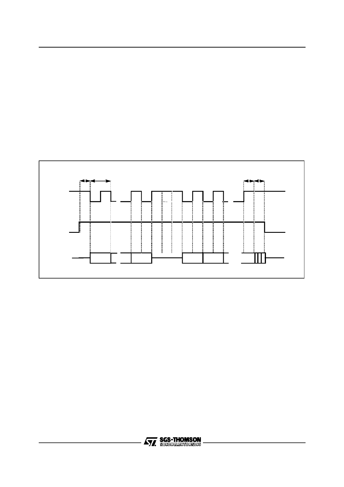
8/16
10 - SYNCHRONOUS SERIAL PORT (ST10R163)
Performing a Read Operation
If the SPRW bit in register SSPCON0 is set, a
read operation is selected. During a read opera-
tion, first information (command or address infor-
mation) is transferred from the CPU (master) to
the slave peripheral. Then the transfer direction is
switched, and information is transferred from the
slave to the master. As for the write operation, the
transmit buffers SSPTB2...SSPTB0 are written by
the CPU with the information data to be first trans-
ferred. Writing to SSPTB0 will start the transfer.
The following figure shows the basic waveforms
for a read operation of the SSP.
For the first part of a read operation (transfer of
SSPTBx from master to slave), the same rules as
for the write operation are applied concerning the
relation between the transfer length and writes in
the Transmit Buffers.After writing to SSPTB0, first
the content of the transmit buffers are shifted out.
Then the data line SSPDAT is switched to input
(high-impedance). After a gap of one bit clock, the
data present at the SSPDAT pin is latched in with
the next 8 clock edges. When the last bit is
clocked in, the chip enable line is deactivated one
half bit time later.
Figure 7-6. Read Operation Waveforms
SSPCLK
SSPCEx
SSPDAT
23/15/7
6
0
0.5
0
1
7
BT
0.5
BT
0.5
BT
1 Bit
Time
Data driven by master
Data driven by slave
178

9/16
10 - SYNCHRONOUS SERIAL PORT (ST10R163)
Chip Enable Lines
Two chip enable lines are provided by the SSP
which are automatically activated at the beginning
of a transfer and deactivated again after the trans-
fer is completed. As shown in the previous figures,
activation of a chip enable line always begins one
half bit time before the first data bit is output at the
SSPDAT pin, and the deactivation (except for con-
tinuous transfers) is performed one half bit time af-
ter the last bit of the transfer has been completely
transmitted/received.
The chip enable lines are selected through the
control bits SSPSEL0 and SSPSEL1. Note that
these automatic chip enable lines can be extend-
ed through normal IO pins, which, however, must
be activated and deactivated through software. To
avoid conflicts with the automatic chip enable
lines, the combination ‘00’ for SSPSEL1..0 disa-
bles these lines, and should be programmed when
using IO lines as additional chip enable signals.
It is also possible to activate both chip enable lines
with the combination ‘11’ for SSPSEL1..0. This
can be used if the same information has to be
transferred
to
several
slaves
simultaneously
(message broadcast), providing that all slave pe-
ripherals use the same clock configuration. Note
that this option should only be used for write oper-
ation, since for read operations, a conflict on the
data line SSPDAT could occur if several slave pe-
ripherals try to drive this line.
Using the SSP Chip Enable and Clock Lines
for Output Functions
Note that the polarity and output control bits direct-
ly influence the lines SSPCLK, SSPCE0 and
SSPCE1, regardless whether a transfer is in
progress or not. It is recommended not to repro-
gram these control bits while a transfer is in
progress to avoid false operation of the addressed
slave peripheral(s).
However, if no transfer is in progress or the SSP is
not used at all, the polarity and output control bit
can be used to perform general purpose output
functions on the pins SSPCLK, SSPCE0 and
SSPCE1. The possible options are:
- output a low level,
- output a high level,
- high-impedance (tri-state). The pin
can be used as a general purpose IO
through Port 4 P4 register if this port
line is configured as an input through
DP4 register.
179
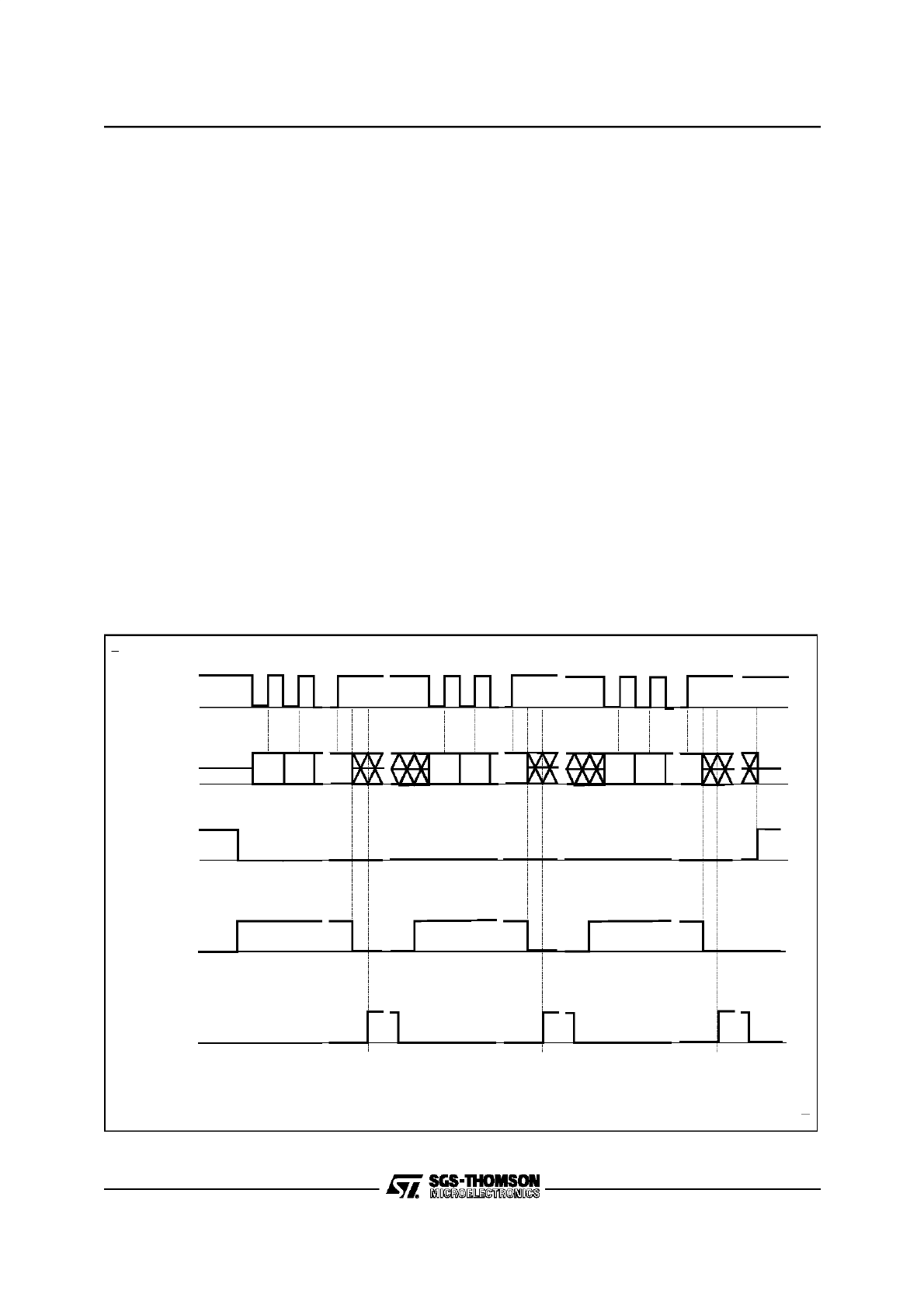
10/16
10 - SYNCHRONOUS SERIAL PORT (ST10R163)
Continuous Transfer Modes
In order to simplify communication with some
standard slave devices such as EEPROMs, a con-
tinuous transfer mode is implemented in the SSP.
This mode is distinguished from the normal mode
in that the chip enable line is not deactivated auto-
matically after a transfer is completed, but instead
remains active until the mode is switched back
from continuous mode (SSPCM = ‘1’) to normal
mode (SSPCM = ‘0’). Thus, consecutive transfers
can be performed while holding the chip enable
line active during the entire procedure. This condi-
tion keeps most peripheral slave devices in the
operational mode initiated through the first com-
mand transfer. EEPROMs, for instance, are
placed into a read mode through first transferring
a read command to it. This command is followed
by the start address of the location to be read. Af-
ter this, the EEPROM transfers the data stored in
the specified address to the master. If now the
chip enable line is deactivated, the EEPROM can-
cels the read mode and returns to idle mode. A
new read operation must again start with the read
command followed by an address, and then the
data byte at this address is returned to the master.
However, if the chip enable line is not deactivated
after the EEPROM has transferred the first data
byte, the EEPROM automatically increments to
the next address location. If now subsequent clock
pulses are applied to the device, the content of
this next location is transferred to the master, and
so on. In this mode, the EEPROM can be continu-
ously read without having to issue the read com-
mand and the start address again.
A similar operation is true for writing to such an
EEPROM. These devices allow a certain number
of data bytes to be written after an initial write com-
mand followed by a start address for the writes.
The figure below shows the write operation in con-
tinuous mode. The TB0_Full flag is again used to
start subsequent writes to the slave device. The
gap between the transfers is application depend-
ent, since the CPU first has to react on the inter-
rupt request at the end of one transfer and rewrite
the transmit buffer registers before the next trans-
fer will start. This procedure continues until the
mode is switched from continuous mode to normal
mode. The chip enable line will then be deactivat-
ed immediately if no transfer is in progress or after
the current transfer is completed.
Figure 7-7. Write Operation Waveforms in Continuous Mode
SSPCLK
SSPDAT
SSPCE0, 1
TB0
Full
SSP
Interrupt
23,
15,7
22,
14,6
Data driven
to Slave
Data driven
to Slave
0
0
23,
15,7
22,
14,6
23,
15,7
22,
14,6
0
Data driven
to Slave
Disable
Continous
Mode
Write
TBO
Write
TBO
Write
TBO
Service
Interrupt
Service
Interrupt
Service
Interrupt
VR02084A
180
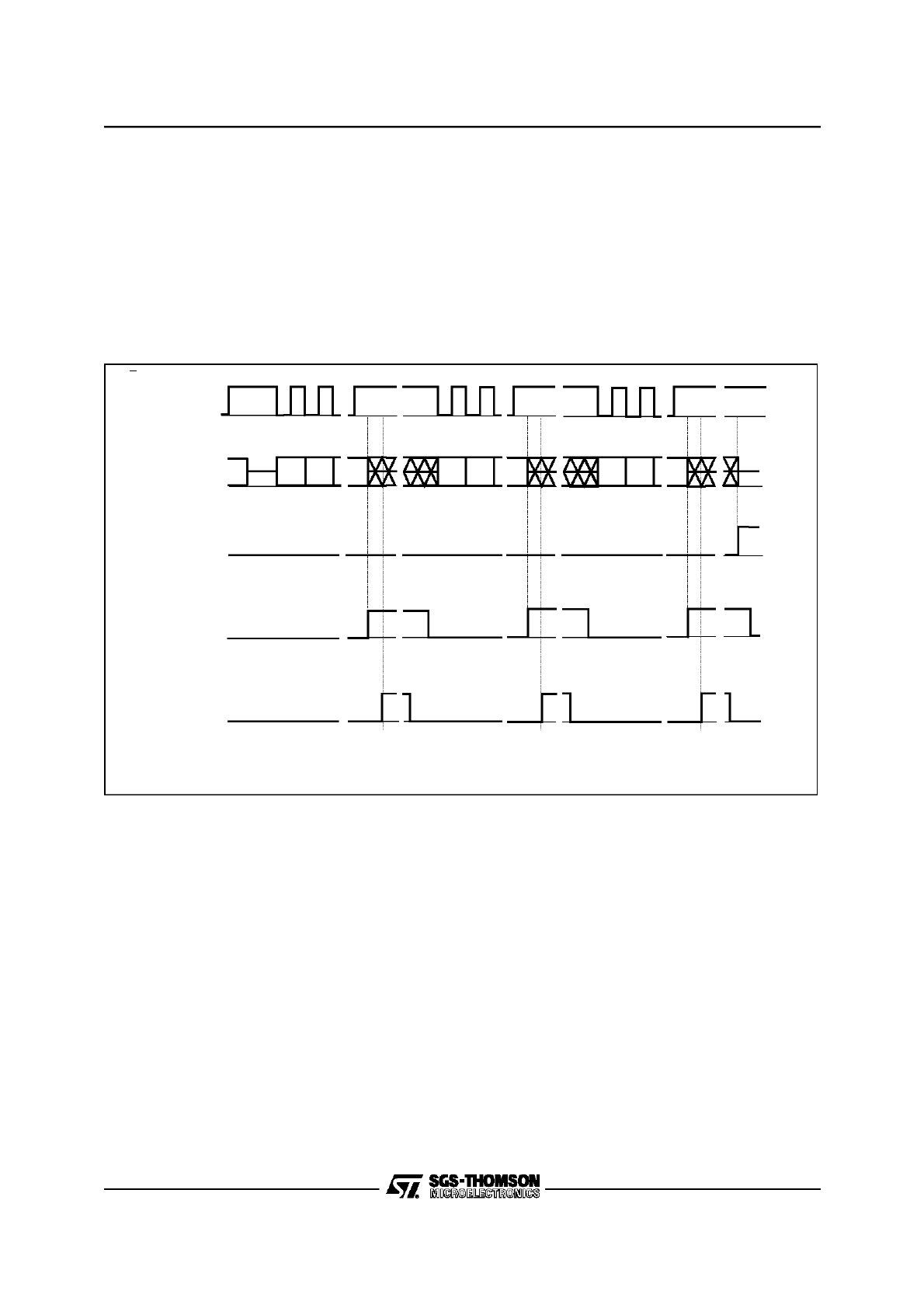
11/16
10 - SYNCHRONOUS SERIAL PORT (ST10R163)
The following figure shows the read operation in
continuous mode. Note that the diagram shown
starts at the point where the master has written the
initial information to the slave and switches the
data line SSPDAT from output to input. At the end
of a transfer, the byte received from the slave is
stored in register SSPRB0, and an internal flag
RB0_Full is set. Reading SSPRB0 through soft-
ware clears this flag, and issues the next 8 clock
pulses to receive the next byte from the slave de-
vice. The time between the transfers depends
again on the application; the CPU has to react on
the interrupt request and read register SSPRB0 in
order to start the next transfer. This procedure
continues until the mode is switched from continu-
ous mode back to normal mode. The chip enable
lines will then be deactivated immediately if no
transfer is in progress or after the current transfer
is completed.
Figure 7-8. Read Operation Waveforms in Continuous Mode
SSPCLK
SSPDAT
SSPCE0, 1
RB0
Full
SSP
Interrupt
7
6
Data driven
to Slave
Data driven
from Slave
0
0
7
6
7
6
0
Data driven
from Slave
Read
RBO
Service
Interrupt
Service
Interrupt
Service
Interrupt
VR02084B
0
Byte n
Byte 1
Byte 0
Read
RBO
Read
RBO
Read
RBO
Data driven
from Slave
181
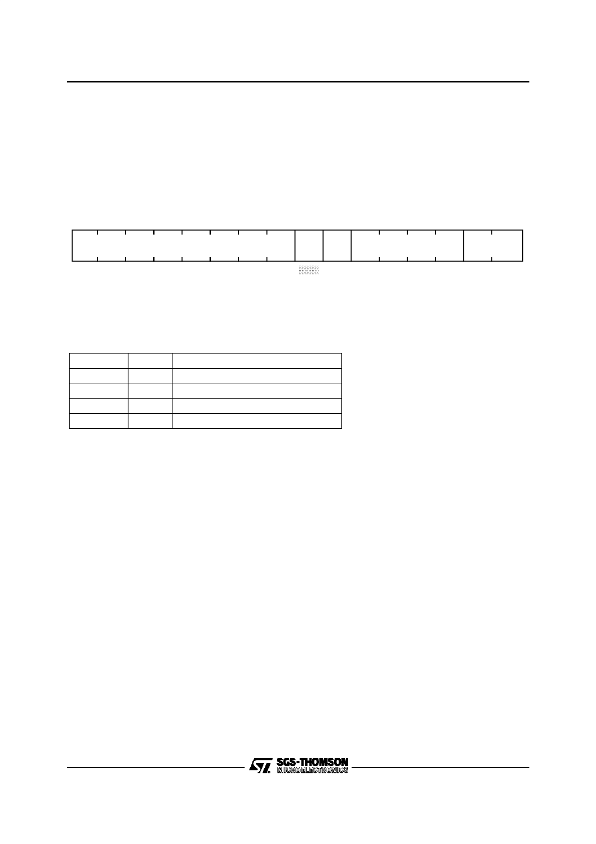
12/16
10 - SYNCHRONOUS SERIAL PORT (ST10R163)
Interrupt Control for the SSP
At the end of a transfer in a read or write opera-
tion, the interrupt request flag XP1IR in register
XP1IC will be set. This will cause an interrupt to
the XP1INT interrupt vector or trigger a PEC serv-
ice, if the interrupt enable bit XP1IE in register
XP1IC is set, or the software can poll the XP1IR
flag. Note that when using polling technique, the
software must clear the XP1IR flag.
The timing for the interrupt request generation is
such that the request bit is set one half bit time af-
ter completion of the last data bit time. In refer-
ence to the normal mode, this is the same time
point where the chip enable line is deactivated.
Note that the distinction between a write or a read
operation interrupt must be performed through
software.
XP1IC (F18Eh)
ESFR
Reset Value: - - 00h
Note: Please refer to the general Interrupt Control Register description for an explanation of the control fields.
SSP Input/Output Pins
The SSP is connected to the external world via
four signals on Port 4:
Note: These SSP signals are only available on the Port 4 pins, if
Port 4 is not programmed to output all 8 segment address lines. Se-
lect 0, 2 or 4 segment address lines (at start-up configuration during
reset) if the SSP is to be used.
5
4
3
2
1
0
11
10
9
8
7
6
15
14
13
12
rw
rw
rw
XP1IR XP1IE
-
-
-
-
-
-
-
-
ILVL
rw
GLVL
SSP Signal Port Pin Function
SSPCLK
P4.7
Clock Line of the SSP.
SSPDAT
P4.6
Data Input/Output Line of the SSP.
SSPCE0
P4.5
Chip Enable Line 0 of the SSP.
SSPCE1
P4.4
Chip Enable Line 1 of the SSP.
182

13/16
10 - SYNCHRONOUS SERIAL PORT (ST10R163)
Accessing the On-chip SSP
The SSP is accessed like an external memory or
peripheral. That means that the registers of the
SSP can be read and written using 16-bit or 8-bit
direct or indirect MEM addressing modes. Since
the XBUS, to witch the SSP is connected, also
represents the external bus, SSP accesses follow
the same rules and procedures as accesses to the
external bus. SSP accesses cannot be executed
in parallel to external instruction fetches or data
read/writes, but are arbitrated and inserted into
the external bus access stream.
However, the on-chip SSP is accessed via the 16-
bit demultiplexed bus mode exclusively. This pro-
vides the user the fastest access to the SSP reg-
isters.
When accessing the on-chip SSP, the bus has to
be switched to the appropriate bus mode within
the SSP address range. This is done via a specific
register-pair, XBCON1 and XADRS1, which is
similar to the BUSCONx/ADDRSELx register-
pairs. With the XBCON1 register (XBUS Bus Con-
figuration Register 1), the bus mode, number of
waitstates, etc., for accessing the SSP are control-
led. The XADRS1 register (XBUS Address Select
Register 1) is used to specify the SSP address ar-
ea. Contrary to the BUSCONx/ADDRSELx regis-
ters, the XBCON1/XADRS1 registers are mask-
programmed, i.e. they are not software program-
mable.
The mask-programming of these registers is:
XBCO N1: 04BFh
XADR S1: 0EF0h
The XBCON1 register is organized like the BUS-
CONx registers except that there is no option for
read/write chip selects (bits 14 and 15). With the
mask-programmed value shown above, the fol-
lowing options are selected:
XRDY EN:0
READY disabled
XBUSACT:1
XBUS active
XALECTL:0
No ALE Lengt hening
XBTYP:10
16-bit DEMUX Bus
XMTTC:1
No Tri- Stat e Wait-
state
XRWDC:1
No Read /Wri te Delay
XMTRC:1101 0 Waits tate
Note: The XBUSACT bit of register XBCON1 only
enables accesses to the SSP, it does not control
the external bus (as the other BUSACT bits in the
BUSCONs).
The XADRS0 register is organized like the other
ADDRSELx registers except that it uses the re-
duced address ranges, which are defined for
XBUS Peripherals. With the mask-programmed
value shown above, the following options are se-
lected:
ADDR: 00’E F00hSSP addres s area
starts at EF00h in segment 0
RGSZ: 0000 SSP address area
covers 256 bytes
Locating the SSP address area to address EF00h
in segment 0 has the advantage that the SSP is
accessible via the data page 3, which is the ‘sys-
tem’ data page, accessed usually through the
‘system’ data page pointer DPP3. In this way, the
internal addresses, such like SFRs, internal RAM,
and the SSP registers, are all located into the
same data page, and form a contiguous address
space.
Visibility of Accesses to the SSP
An access to the SSP can be made fully visible ex-
ternally or not. This option is controlled by the bit
VISIBLE in register SYSCON. The grade of visibil-
ity depends on several conditions described in the
following.
183

14/16
10 - SYNCHRONOUS SERIAL PORT (ST10R163)
Single Chip Mode
Since the ST10R163 is a ROMless device, it can
not be run in single chip mode. This description is
only intended for future version that could provide
internal Flash or ROM. The single chip mode is
entered during reset with pin EA tied to a logic
high level. The chip will start running in single chip
mode without an external bus.
When bit VISIBLE in register SYSCON is cleared,
SSP accesses will be completely hidden. Al-
though the SSP is connected to the XBUS, which
is an internal implementation of the external bus, it
can be accessed in single chip mode without any
restriction. No external bus signal will be generat-
ed for an access to the SSP address range, be-
cause the XBUSACT bit in register XBCON1 only
controls accesses to the SSP via the XBUS, it
does not control the external bus (i.e. PORT0,
PORT1, Port 4 and Port 6 can be used for general
purpose I/O).
When bit VISIBLE in register SYSCON is set, then
accesses to the SSP can be made visible to the
external world. To do so, one of the BUSCON reg-
isters has to enable a 16-bit demultiplexed exter-
nal bus (PORT0 and PORT1 cannot be used for
general purpose I/O in this case). All accesses to
the SSP can be monitored externally,
and
read/write strobes are generated. The visibility of
the segment address depends on the number of
segment address lines selected for Port 4.
External Bus Mode
If an external bus is enabled through one or more
of the BUSCON registers, PORT0, PORT1, Port 4
and Port 6 (or parts of them) may be used to con-
trol the external bus.
When bit VISIBLE in register SYSCON is cleared,
accesses to the SSP will be partly reflected on the
external bus. Due to severe timing constraints, it is
not possible to hide SSP accesses completely,
when an external bus is enabled. SSP accesses
will be reflected on the external bus in the follow-
ing manner:
– The ALE signal will be generated in any case.
– No Read or Write Signals will be generated.
– The data of a read access cannot be seen.
– The visibility of the segment address depends
on the number of segment address lines se-
lected for Port 4.
– The SSP is connected to the bus controller via
a 16-bit demultiplexed bus. However, address
and data information of a SSP access will be
only on those ports operating in the currently
selected bus mode, as shown in the table be-
low.
When bit VISIBLE in register SYSCON is set, full
visibility of all SSP accesses is provided, if a 16-bit
demultiplexed bus mode is enabled through one
of the BUSCON registers (PORT0 and PORT1
cannot be used for general purpose I/O in this
case). All SSP accesses can be monitored exter-
nally and read/write strobes are generated. The
visibility of the segment address depends on the
number of segment address lines selected for Port
4.
Currently Selected Bus Mode Port
Visible Information of SSP Access
8-bit Multiplexed
P0L
Low Byte of SSP Write Data
P0H
High Byte of SSP Write Data
8-bit Demultiplexed
P0L
Low Byte of SSP Write Data (High byte not visible)
PORT1
16-bit SSP Address
16-bit Multiplexed
PORT0
16-bit SSP Write Data
16-bit Demultiplexed
PORT0
16-bit SSP Write Data
PORT1
16-bit SSP Address
184

15/16
10 - SYNCHRONOUS SERIAL PORT (ST10R163)
Accessing the SSP in Hold Mode
When the ST10R163 is placed into hold mode by
an external HOLD request, accesses to external
memory or peripherals have to wait until the
HOLD request is deactivated. SSP accesses,
however, can be executed in this mode, if bit VIS-
IBLE in register SYSCON is cleared. In this case,
an access to the SSP is completely invisible to the
external world. If bit VISIBLE is set, then also SSP
accesses have to wait until the external HOLD re-
quest is removed.
Note: SSP accesses during HOLD mode are
blocked after any attempt to access an external lo-
cation, even if the VISIBLE bit is cleared. The initi-
ated external access must be finished first, which
requires the HOLD condition to be removed.
Power Down Mode
If the ST10R163 enters the Power Down Mode,
the XCLK (XBUS Clock) signal will be turned off
which will stop the operation of the SSP. Any
transfer operation in progress will be interrupted.
After returning from Power Down Mode via hard-
ware reset, the SSP has to be reconfigured.
185

16/16
10 - SYNCHRONOUS SERIAL PORT (ST10R163)
Notes:
186
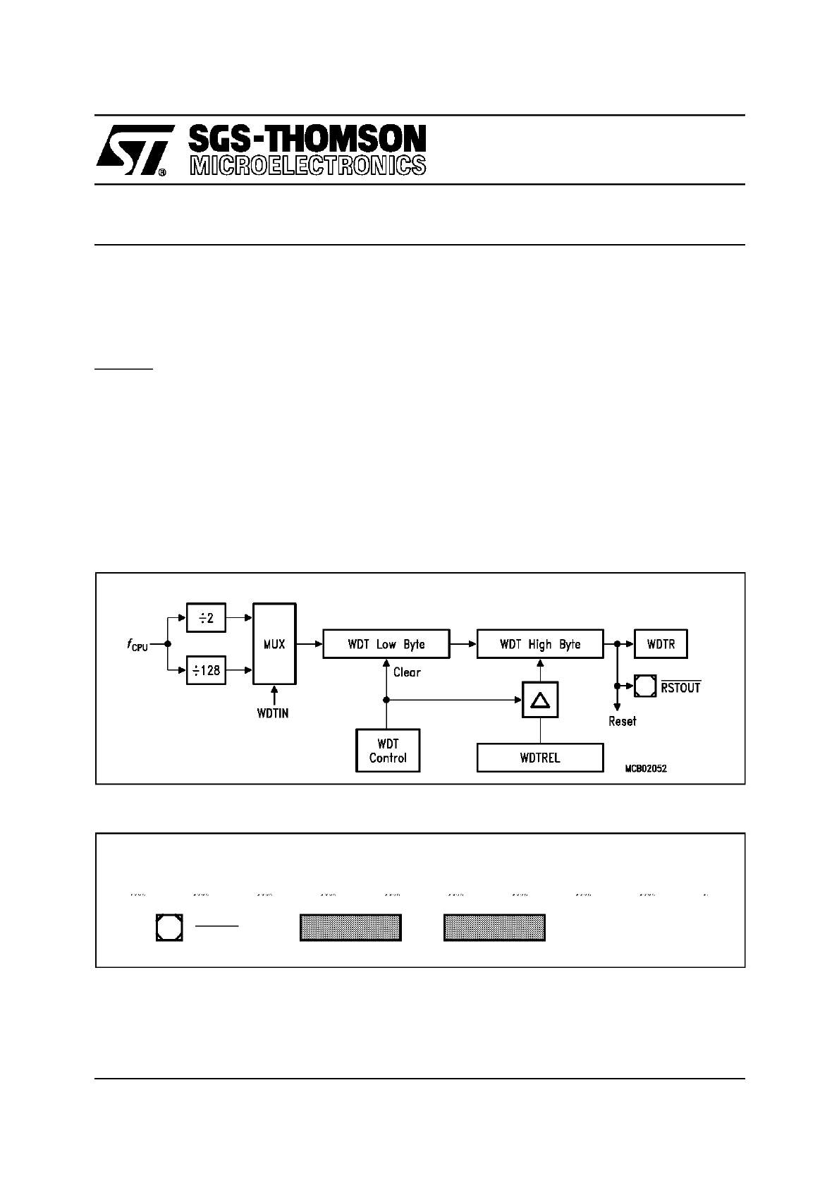
February 1996
1/4
This is advance information from SGS-TH OMSON. Details are subject tochange without notice.
ST10R163
User Manual
11 - WATCHDOG TIMER
To allow recovery from software or hardware fail-
ure, the ST10R163 provides a Watchdog Timer. If
the software fails to service this timer before an
overflow occurs, an internal reset sequence will be
initiated. This internal reset will also pull the
RSTOUT pin low, which also resets the peripheral
hardware, which might be the cause for the mal-
function. When the watchdog timer is enabled and
the software has been designed to service it regu-
larly before it overflows, the watchdog timer will
supervise the program execution, as it only will
overflow if the program does not progress proper-
ly. The watchdog timer will also time out, if a soft-
ware error was due to hardware related failures.
This prevents the controller from malfunctioning
for longer than a user-specified time.
The watchdog timer provides two registers: a
read-only timer register that contains the current
count, and a control register for initialization.
The watchdog timer is a 16-bit up counter which
can be clocked with the CPU clock (
fCPU) either
divided by 2 or divided by 128. This 16-bit timer is
realized as two concatenated 8-bit timers (see fig-
ure below). The upper 8 bits of the watchdog timer
can be preset to a user-programmable value via a
watchdog service access in order to vary the
watchdog expire time. The lower 8 bits are reset
on each service access.
Figure 8-1. Watchdog Timer Block Diagram
Figure 8-2.
SFRs and Port Pins associated with the Watchdog Timer
WDTCON
RSTOU T
Reset Indication Pin
Data Registers
Control Registers
WDT
187
2/4
11 - WATCHDOG TIMER (ST10R163)
Operation of the Watchdog Timer
The current count value of the Watchdog Timer is
contained in the Watchdog Timer Register WDT,
which is a non-bitaddressable read-only register.
The operation of the Watchdog Timer is controlled
by its bitaddressable Watchdog Timer Control
Register WDTCON. This register specifies the re-
load value for the high byte of the timer, selects
the input clock prescaling factor and provides a
flag that indicates a watchdog timer overflow.
After any software reset, external hardware reset
(see note), or watchdog timer reset, the watchdog
timer is enabled and starts counting up from
0000h with the frequency
fCPU/2. The input fre-
quency may be switched to
fCPU/128 by setting
bit WDTIN. The watchdog timer can be disabled
via the instruction DISWDT (Disable Watchdog
Timer). Instruction DISWDT is a protected 32-bit
instruction which will ONLY be executed during
the time between a reset and execution of either
the EINIT (End of Initialization) or the SRVWDT
(Service Watchdog Timer) instruction. Either one
of these instructions disables the execution of
DISWDT.
When the watchdog timer is not disabled via in-
struction DISWDT, it will continue counting up,
even during Idle Mode. If it is not serviced via the
instruction SRVWDT by the time the count reach-
es FFFFh the watchdog timer will overflow and
cause an internal reset. This reset will pull the ex-
ternal reset indication pin RSTOUT low. It differs
from a software or external hardware reset in that
bit WDTR (Watchdog Timer Reset Indication Flag)
of register WDTCON will be set. A hardware reset
or the SRVWDT instruction will clear this bit. Bit
WDTR can be examined by software in order to
determine the cause of the reset.
A watchdog reset will also complete a running ex-
ternal bus cycle before starting the internal reset
sequence if this bus cycle does not useREADY or
samples READY active (low) after the pro-
grammed waitstates. Otherwise the external bus
cycle will be aborted.
Note: After a hardware reset that activates the
Bootstrap Loader the watchdog timer will be disa-
bled
To prevent the watchdog timer from overflowing, it
must be serviced periodically by the user soft-
ware. The watchdog timer is serviced with the in-
struction SRVWDT, which is a protected 32-bit in-
struction. Servicing the watchdog timer clears the
low byte and reloads the high byte of the watch-
dog time register WDT with the preset value in bit
field WDTREL, which is the high byte of register
WDTCON. Servicing the watchdog timer will also
reset bit WDTR. After being serviced the watch-
dog timer continues counting up from the value
(<WDTREL> * 2
8
). Instruction SRVWDT has been
encoded in such a way that the chance of uninten-
tionally servicing the watchdog timer (eg. by fetch-
ing and executing a bit pattern from a wrong loca-
tion) is minimized. When instruction SRVWDT
does not match the format for protected instruc-
tions, the Protection Fault Trap will be entered,
rather than the instruction be executed.
WDTCON (FFAEh / D7h)
SFR
Reset Value: 000Xh
Note: The reset value will be 0002h, if the reset was triggered by the watchdog timer (overflow). It will be 0000h other-
wise.
Bit
Function
WDTIN
Watchdog Timer Input Frequency Selection
‘0’: Input frequency is f
CPU
/ 2
‘1’: Input frequency is f
CPU
/ 128
WDTR
Watchdog Timer Reset Indication Flag
Set by the watchdog timer on an overflow.
Cleared by a hardware reset or by the SRVWDT instruction.
WDTREL
Watchdog Timer Reload Value
(for the high byte)
-
WDT
R
-
WDT
IN
-
-
-
-
5
4
3
2
1
0
11
10
9
8
7
6
15
14
13
12
-
-
-
r
rw
-
-
WDTREL
-
rw
188
3/4
11 - WATCHDOG TIMER (ST10R163)
The time period for an overflow of the watchdog
timer is programmable in two ways:
•
the input frequency to the watchdog timer can
be selected via bit WDTIN in register WDTCON
to be either
fCPU/2 or fCPU/128.
•
the reload value WDTREL for the high byte of
WDT can be programmed in register WDTCON.
The period P
WDT
between servicing the watchdog
timer and the next overflow can therefore be de-
termined by the following formula:
The table below marks the possible ranges for the
watchdog time which can be achieved using a
CPU clock of 20 MHz. Some numbers are round-
ed to 3 significant digits.
Note: For safety reasons, the user is advised to
rewrite WDTCON each time before the watchdog
timer is serviced.
P
WDT
=
f
CPU
2
(1 + <WDTIN>*6)
* (2
16
- <WDTREL> * 2
8
)
Reload value
in WDTREL
Prescaler for f
CPU
2 (WDTIN = ‘0’)
128 (WDTIN = ‘1’)
FFh
25.6 ms
1.6 ms
00h
6.55 ms
419 ms
189

4/4
11 - WATCHDOG TIMER (ST10R163)
Note:
190
February 1996
1/8
This is advance information from SGS-TH OMSON. Details are subject tochange without notice.
ST10R163
User Manual
12 - SYSTEM RESET
The internal system reset function provides initial-
ization of the ST10R163 into a defined default
state and is invoked either by asserting a hard-
ware reset signal on pin RSTIN (Hardware Reset
Input), upon the execution of the SRST instruction
(Software Reset) or by an overflow of the watch-
dog timer
Whenever one of these conditions occurs, the mi-
crocontroller is reset into its predefined default
state through an internal reset procedure. When a
reset is initiated, pending internal hold states are
cancelled and the current internal access cycle (if
any) is completed. An external bus cycle is abort-
ed, except for a watchdog reset (see description).
After that the bus pin drivers and the IO pin drivers
are switched off (tristate). RSTOUT is activated
depending on the reset source.
The internal reset procedure requires 516 CPU
clock cycles (25.8
µ
s @ 20 MHz CPU clock) in or-
der to perform a complete reset sequence. This
516 cycle reset sequence is started upon a watch-
dog timer overflow, a SRST instruction or when
the reset input signal RSTIN is latched low (hard-
ware reset). The internal reset condition is active
at least for the duration of the reset sequence and
then until the RSTIN input is inactive. When this
internal reset condition is removed (reset se-
quence complete and RSTIN inactive), the reset
configuration is latched from PORT0, and pins
ALE, RD and WR are driven to their inactive lev-
els.
After the internal reset condition is removed, the
microcontroller will start program execution from
memory location 00’0000h in code segment zero.
This start location will typically hold a branch in-
struction to the start of a software initialization rou-
tine for the application specific configuration of pe-
ripherals and CPU Special Function Registers.
Figure 9-1. External Reset Circuitry
ST10R163
Reset
V
CC
External
Hardware
RSTOUT
&
External
Reset
Sources
+
a) Generated Warm reset
b) Automatic Power-on reset
191

2/8
12 - SYSTEM RESET (ST10R163)
Hardware Reset
A hardware reset is triggered when the reset input
signal RSTIN is latched low. To ensure the recog-
nition of the RSTIN signal (latching), it must be
held low for at least 2 CPU clock cycles. However,
also shorter RSTIN pulses may trigger a hardware
reset, if they coincide with the latch’s sample
point. RSTIN may go high during the reset se-
quence. After the reset sequence has been com-
pleted, the RSTIN input is sampled. When the re-
set input signal is active at that time the internal re-
set condition is prolonged until RSTIN gets inac-
tive.
The input RSTIN provides an internal pullup de-
vice equalling a resistor of 50 K
Ω
to 150 K
Ω
(the
minimum reset time must be determined by the
lowest value). Simply connecting an external ca-
pacitor is sufficient for an automatic power-on re-
set (see a) in figure above). RSTIN may also be
connected to the output of other logic gates (see
b) in figure above).
Note: Driving RSTIN low for 2 CPU clock cycles is
only sufficient for a hardware triggered warm re-
set. A power-on reset requires an active time of
two reset sequences (1036 CPU clock cycles) af-
ter a stable clock signal is available (about 10...50
ms to allow the on-chip oscillator to stabilize).
Software Reset
The reset sequence can be triggered at any time
via the protected instruction SRST (Software Re-
set). This instruction can be executed deliberately
within a program, eg. to leave bootstrap loader
mode, or upon a hardware trap that reveals a sys-
tem failure.
A software reset disregards the configuration of
P0L.5...P0L.0.
Watchdog Timer Reset
When the watchdog timer is not disabled during
the initialization or serviced regularly during pro-
gram execution is will overflow and trigger the re-
set sequence. Other than hardware and software
reset the watchdog reset completes a running ex-
ternal bus cycle if this bus cycle either does not
use READY at all, or if READY is sampled active
(low) after the programmed waitstates. When
READY is sampled inactive (high) after the pro-
grammed waitstates the running external bus cy-
cle is aborted. Then the internal reset sequence is
started.
Note: A watchdog reset disregards the configura-
tion of P0L.5...P0L.0.
The watchdog reset cannot occur while the
ST10R163 is in bootstrap loader mode!
192
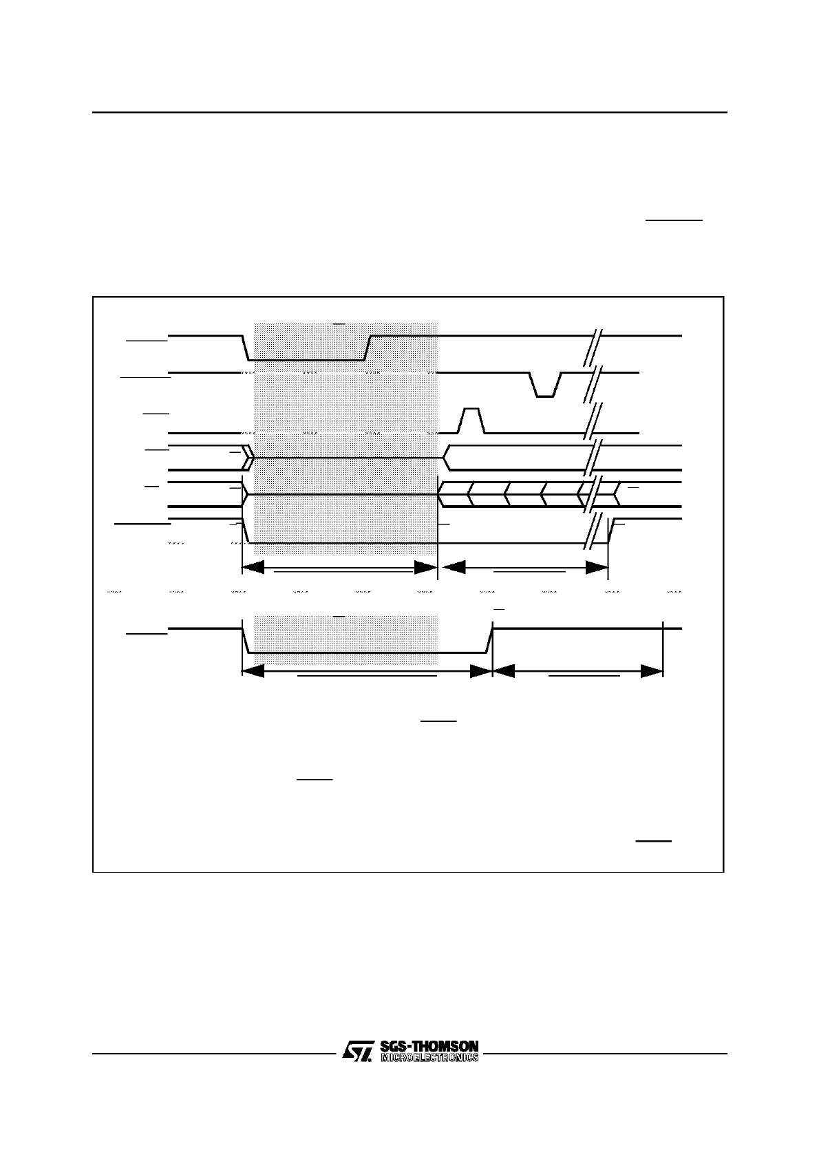
3/8
12 - SYSTEM RESET (ST10R163)
12.1 THE ST10R163’S PINS AFTER RESET
After the reset sequence the different groups of
pins of the ST10R163 are activated in different
ways depending on their function. Bus and control
signals are activated immediately after the reset
sequence according to the configuration latched
from PORT0, so either external accesses can
takes place or the external control signals are in-
active. The general purpose IO pins remain in in-
put mode (high impedance) until reprogrammed
via software (see figure below). TheRSTOUT pin
remains active (low) until the end of the initializa-
tion routine (see description).
Figure 9-2. Reset Input and Output Signals
RSTOUT
RSTIN
1)
1. Current bus cycle is completed or aborted.
2. Switches asynchronously with RSTIN, synchronously upon software or watchdog reset.
3. The reset condition ends here. The ST10R163 starts program execution.
4. Activation of the IO pins is controlled by software.
5. Execution of the EINIT instruction.
6. The shaded area designates the internal reset sequence, which starts after synchronization of RSTIN.
Internal reset condition
3)
Initialization
6)
Bus
Internal reset condition
Initialization
ALE
RD, WR
RSTIN
2)
IO
2
)
3)
5)
4)
6)
When the internal reset condition is prolongued by RSTIN, the activation of the outp ut signals is
delayed until the end of the internal reset condition .
193

4/8
12 - SYSTEM RESET (ST10R163)
12.2 RESET OUTPUT PIN
The RSTOUT pin is dedicated to generate a reset
signal for the system components besides the
controller itself. RSTOUT will be driven active
(low) at the begin of any reset sequence (triggered
by hardware, the SRST instruction or a watchdog
timer overflow). RSTOUT stays active (low) be-
yond the end of the internal reset sequence until
the protected EINIT (End of Initialization) instruc-
tion is executed (see figure above). This allows to
completely configure the controller including its
on-chip peripheral units before releasing the reset
signal for the external peripherals of the system.
12.3 WATCHDOG TIMER OPERATION AFTER
RESET
The watchdog timer starts running after the inter-
nal reset has completed. It will be clocked with the
internal system clock divided by 2 (10 MHz @
fCPU=20 MHz), and its default reload value is
00h, so a watchdog timer overflow will occur
131072 CPU clock cycles (6.55 ms @
fCPU=20
MHz) after completion of the internal reset, unless
it is disabled, serviced or reprogrammed mean-
while. When the system reset was caused by a
watchdog timer overflow, the WDTR (Watchdog
Timer Reset Indication) flag in register WDTCON
will be set to ’1’. This indicates the cause of the in-
ternal reset to the software initialization routine.
WDTR is reset to ’0’ by an external hardware reset
or by servicing the watchdog timer. After the inter-
nal reset has completed, the operation of the
watchdog timer can be disabled by the DISWDT
(Disable Watchdog Timer) instruction. This in-
struction has been implemented as a protected in-
struction. For further security, its execution is only
enabled in the time period after a reset until either
the SRVWDT (Service Watchdog Timer) or the
EINIT instruction has been executed. Thereafter
the DISWDT instruction will have no effect.
12.4 RESET VALUES FOR THE ST10R163
REGISTERS
During the reset sequence the registers of the
ST10R163 are preset with a default value. Most
SFRs, including system registers and peripheral
control and data registers, are cleared to zero, so
all peripherals and the interrupt system are off or
idle after reset. A few exceptions to this rule pro-
vide a first pre-initialization, which is either fixed or
controlled by input pins.
DPP1:0001h (points to data page 1)
DPP2:0002h (points to data page 2)
DPP3:0003h (points to data page 3)
CP: FC00h
STKUN:FC00h
STKOV:FA00h
SP: FC00h
WDTCON:0002h, if reset was triggered by
a watchdog timer overflow, 0000h
otherwise
S0RBUF:XXh (undefined)
SSCRB:XXXXh (undefined)
SYSCON:0XX0h (set according to reset
configuration)
BUSCON0:0XX0h (set according to reset
configuration)
RP0H:XXh (reset levels of P0H)
ONES:FFFFh (fixed value)
12.5 THE INTERNAL RAM AFTER RESET
The contents of the internal RAM are not affected
by a system reset. However, after a power-on re-
set, the contents of the internal RAM are unde-
fined. This implies that the GPRs (R15...R0) and
the
PEC
source
and
destination
pointers
(SRCP7...SRCP0, DSTP7...DSTP0) which are
mapped into the internal RAM are also unchanged
after a warm reset, software reset or watchdog re-
set, but are undefined after a power-on reset.
12.6
PORTS
AND
EXTERNAL
BUS
CONFIGURATION DURING RESET
During the internal reset sequence all of the
ST10R163’s port pins are configured as inputs by
clearing the associated direction registers, and
their pin drivers are switched to the high imped-
ance state. This ensures that the ST10R163 and
external devices will not try to drive the same pin
to different levels. Pin ALE is held low through an
internal pulldown, and pins RD and WR are held
high through internal pullups. Also the pins select-
ed for CS output will be pulled high.
The registers SYSCON and BUSCON0 are initial-
ized according to the configuration selected via
PORT0.
194

5/8
12 - SYSTEM RESET (ST10R163)
PORTS AND EXTERNAL BUS CONFIGURATION DURING RESET(Cont’d)
Pin EA must be held at ‘0’ level.
•
the Bus Type field (BTYP) in register BUSCON0
is initialized according to P0L.7 and P0L.6
•
bit BUSACT0 in register BUSCON0 is set to ‘1’
•
bit ALECTL0 in register BUSCON0 is set to ‘1’
•
bit ROMEN in register SYSCON will be cleared
to ‘0’
•
bit BYTDIS in register SYSCON is set according
to the data bus width
The other bits of register BUSCON0, and the other
BUSCON registers are cleared. This default initial-
ization selects the slowest possible external ac-
cesses using the configured bus type. The Ready
function is disabled at the end of the internal sys-
tem reset.
When the internal reset has completed, the config-
uration of PORT0, PORT1, Port 4, Port 6 and of
the BHE signal (High Byte Enable, alternate func-
tion of P3.12) depends on the bus type which was
selected during reset. When any of the external
bus modes was selected during reset, PORT0
(and PORT1) will operate in the selected bus
mode. Port 4 will output the selected number of
segment address lines (all zero after reset) and
Port 6 will drive the selected number ofCS lines
(CS0 will be ‘0’, while the other activeCS lines will
be ‘1’). When no memory accesses above 64 K
are to be performed, segmentation may be disa-
bled.
All other pins remain in the high-impedance state
until they are changed by software or peripheral
operation.
12.7 APPLICATION-SPECIFIC INITIALIZATION
ROUTINE
After the internal reset condition is removed the
ST10R163 fetches the first instruction from loca-
tion 00’0000h, which is the first vector in the
trap/interrupt vector table, the reset vector. 4
words (locations 00’0000h through 00’0007h) are
provided in this table to start the initialization after
reset. As a rule, this location holds a branch in-
struction to the actual initialization routine that
may be located anywhere in the address space.
After reset, it may be desirable to reconfigure the
external bus characteristics, because the SY-
SCON register is initialized during reset to the
slowest possible memory configuration.
To decrease the number of instructions required
to initialize the ST10R163, each peripheral is pro-
grammed to a default configuration upon reset,
but is disabled from operation. These default con-
figurations can be found in the descriptions of the
individual peripherals.
During the software design phase, portions of the
internal memory space must be assigned to regis-
ter banks and system stack. When initializating
the stack pointer (SP) and the context pointer
(CP), it must be ensured that these registers are
initialized before any GPR or stack operation is
performed. This includes interrupt processing,
which is disabled upon completion of the internal
reset, and should remain disabled until the SP is
initialized.
Note: Traps (incl. NMI) may occur, even though
the interrupt system is still disabled.
In addition, the stack overflow (STKOV) and the
stack underflow (STKUN) registers should be ini-
tialized. After reset, the CP, SP, and STKUN reg-
isters all contain the same reset value 00’FC00h,
while the STKOV register contains 00’FA00h.
With the default reset initialization, 256 words of
system stack are available, where the system
stack selected by the SP grows downwards from
00’FBFEh, while the register bank selected by the
CP grows upwards from 00’FC00h.
Based on the application, the user may wish to in-
itialize portions of the internal memory before nor-
mal program operation. Once the register bank
has been selected by programming the CP regis-
ter, the desired portions of the internal memory
can easily be initialized via indirect addressing.
At the end of the initialization, the interrupt system
may be globally enabled by setting bit IEN in reg-
ister PSW. Care must be taken not to enable the
interrupt system before the initialization is com-
plete.
The software initialization routine should be termi-
nated with the EINIT instruction. This instruction
has been implemented as a protected instruction.
Execution of the EINIT instruction disables the ac-
tion of the DISWDT instruction, disables write ac-
cesses to register SYSCON (see note) and caus-
es the RSTOUT pin to go high. This signal can be
used to indicate the end of the initialization routine
and the proper operation of the microcontroller to
external hardware.
Note: All configurations regarding register SY-
SCON (enable CLKOUT, stacksize, etc.) must be
selected before the execution of EINIT.
195
6/8
12 - SYSTEM RESET (ST10R163)
APPLICATION-SPECIFIC INITIALIZATION ROUTINE(Cont’d)
System Startup Configuration
Although most of the programmable features of
the ST10R163 are either selected during the ini-
tialization phase or repeatedly during program ex-
ecution, there are some features that must be se-
lected earlier, because they are used for the first
access of the program execution (eg. external bus
configuration).
These selections are made during reset via the
pins of PORT0, which are read during the internal
reset sequence. During reset internal pullup devic-
es are active on the PORT0 lines, so their input
level is high, if the respective pin is left open, or is
low, if the respective pin is connected to an exter-
nal pulldown device. The coding of the selections,
as shown below, allows in many cases to use the
default option, ie. high level.
The value on the upper byte of PORT0 (P0H) is
latched into register RP0H upon reset, the value
on the lower byte (P0L) directly influences the
BUSCON0 register (bus mode) or the internal
control logic of the ST10R163.
The pins that control the operation of the internal
control logic and the reserved pins are evaluated
only during a hardware triggered reset sequence.
The pins that influence the configuration of the
ST10R163 are evaluated during any reset se-
quence, ie. also during software and watchdog
timer triggered resets.
The configuration via P0H is latched in register
RP0H for subsequent evaluation by software.
Register RP0H is described in chapter “The Exter-
nal Bus Interface”.
Note: The reserved pins (marked “R”) must re-
main high during reset in order to ensure proper
operation of the ST10R163. The load on those
pins must be small enough for the internal pullup
device to keep their level high, or external pullup
devices must ensure the high level.
The pins marked “X” should be left open for
ST10R163 devices that do not use them.
The following describes the different selections
that are offered for reset configuration. The default
modes refer to pins at high level, ie. without exter-
nal pulldown devices connected. Please also con-
sider the note (above) on reserved pins.
Figure 9-3. PORT0 Configuration during Reset
R
R
R
EMU
ADP
R
WRCFG
L.5
L.4
L.3
L.2
L.1
L.0
H.3
H.2
H.1
H.0
L.7
L.6
H.7
H.6
H.5
H.4
CSSEL
SALSEL
BUSTYP
RP0H
System Clock
Logic
Port 4
Logic
Port 6
Logic
SYSCON
BUSCON0
Internal Control Logic
(Only on hardware reset)
CLKSEL
196

7/8
12 - SYSTEM RESET (ST10R163)
APPLICATION-SPECIFIC INITIALIZATION ROUTINE(Cont’d)
Emulation Mode
Pin P0L.0 (EMU) selects the Emulation Mode,
when low during reset. This mode allows the ac-
cess to integrated XBUS peripherals via the exter-
nal bus interface pins in application specific ver-
sions of the ST10R163.
This mode is used for special emulator purposes
and is of no use in basic ST10R163 devices, so in
this case P0L.0 should be held high.
Default: Emulation Mode is off.
Adapt Mode
Pin P0L.1 (ADP) selects the Adapt Mode, when
low during reset. In this mode the ST10R163 goes
into a passive state, which is similar to its state
during reset. The pins of the ST10R163 float to
tristate or are deactivated via internal pullup/pull-
down devices, as described for the reset state. In
addition also the RSTOUT pin floats to tristate
rather than be driven low, and the on-chip oscilla-
tor is switched off.
This mode allows to switch a ST10R163 that is
mounted to a board virtually off, so an emulator
may control the board’s circuitry, even though the
original ST10R163 remains in its place. The origi-
nal ST10R163 also may resume to control the
board after a reset sequence with P0L.1 high.
Default: Adapt Mode is off.
Note: When XTAL1 is fed by an external clock
generator (while XTAL2 is left open), this clock
signal may also be used to drive the emulator de-
vice.
However, if a crystal is used, the emulator de-
vice’s oscillator can use this crystal only, if at least
XTAL2 of the original device is disconnected from
the circuitry (the output XTAL2 will still be active in
Adapt Mode).
System Clock Configuration
Pins P0H.7 to P0H.5 (PLLSEL) selects the Sys-
tem Clock Configuration at reset. The System
Clock (CPU Clock) can be selected to be 0.5, 1, 2,
2.5, 3, 4 or 5 times the externally applied frequen-
cy at the XTAL-pins. The required system config-
uration setups are described in more details in
chapter “System Clock Generator”.
External Bus Type
Pins P0L.7 and P0L.6 (BUSTYP) select the exter-
nal bus type during reset. This allows to configure
the external bus interface of the ST10R163 even
for the first code fetch after reset. The two bits are
copied into bit field BTYP of register BUSCON0.
P0L.7 controls the data bus width, while P0L.6
controls the address output (multiplexed or demul-
tiplexed). This bit field may be changed via soft-
ware after reset, if required.
PORT0 and PORT1 are automatically switched to
the selected bus mode. In multiplexed bus modes
PORT0 drives both the 16-bit intra-segment ad-
dress and the output data, while PORT1 remains
in high impedance state as long as no demulti-
plexed bus is selected via one of the BUSCON
registers. In demultiplexed bus modes PORT1
drives the 16-bit intra-segment address, while
PORT0 or P0L (according to the selected data bus
width) drives the output data.
For a 16-bit data bus BHE is automatically ena-
bled, for an 8-bit data bus BHE is disabled via bit
BYTDIS in register SYSCON.
Default: 16-bit data bus with multiplexed address-
es.
Note: ST10R165 being a ROMless device, pinEA
must be connected to ground (external start).
197

8/8
12 - SYSTEM RESET (ST10R163)
APPLICATION-SPECIFIC INITIALIZATION ROUTINE(Cont’d)
Chip Select Lines
Pins P0H.2 and P0H.1 (CSSEL) define the
number of active chip select signals during reset.
This allows to control which pins of Port 6 drive ex-
ternal CS signals and which are used for general
purpose IO. The two bits are latched in register
RP0H.
Default: All 5 chip select lines active (CS4...CS0).
Note: The selected number of CS signals cannot
be changed via software after reset.
Segment Address Lines
Pins P0H.4 and P0H.3 (SALSEL) define the
number of active segment address lines during re-
set. This allows to control which pins of Port 4
drive address lines and which are used for general
purpose IO. The two bits are latched in register
RP0H. Depending on the system architecture the
required address space is chosen and accessible
right from the start, so the initialization routine can
directly access all locations without prior program-
ming. The required pins of Port 4 are automatically
switched to address output mode.
Even if not all segment address lines are enabled
on Port 4, the ST10R163 internally uses its com-
plete 24-bit addressing mechanism. This allows to
restrict the width of the effective address bus,
while still deriving CS signals from the complete
addresses.
Default: 2-bit segment address (A17...A16) allow-
ing access to 256 KByte.
Note: The selected number of segment address
lines cannot be changed via software after reset.
BHE Pin Configuration
Pin P0H.0 defines the write configuration control
(bit WRCFG of SYSCON register). If P0H.0 is
pulled down during reset, the bit WRCFG is set to
‘1’ and the pin BHE is configured as WRH (Write
High Byte) while pin WR is configured as WRL
(Write Low Byte). Default: pins WR and BHE re-
tain their normal functions.
198
February 1996
1/4
This is advance information from SGS-TH OMSON. Details are subject tochange without notice.
ST10R163
User Manual
13 - POWER REDUCTION MODES
Two different power reduction modes with differ-
ent levels of power reduction have been imple-
mented in the ST10R163, which may be entered
under software control.
In Idle mode the CPU is stopped, while the pe-
ripherals continue their operation. Idle mode can
be terminated by any reset or interrupt request.
In Power Down mode both the CPU and the pe-
ripherals are stopped. Power Down mode can
only be terminated by a hardware reset.
Note: All external bus actions are completed be-
fore Idle or Power Down mode is entered. Howev-
er, Idle or Power Down mode is not entered if
READY is enabled, but has not been activated
(driven low) during the last bus access.
13.1 IDLE MODE
The power consumption of the ST10R163 micro-
controller can be decreased by entering Idle
mode. In this mode all peripherals, including the
watchdog timer, continue to operate normally,
only the CPU operation is halted.
Idle mode is entered after the IDLE instruction has
been executed and the instruction before the IDLE
instruction has been completed. To prevent unin-
tentional entry into Idle mode, the IDLE instruction
has been implemented as a protected 32-bit in-
struction.
Idle mode is terminated by interrupt requests from
any enabled interrupt source whose individual In-
terrupt Enable flag was set before the Idle mode
was entered, regardless of bit IEN.
For a request selected for CPU interrupt service
the associated interrupt service routine is entered
if the priority level of the requesting source is high-
er than the current CPU priority and the interrupt
system is globally enabled. After the RETI (Return
from Interrupt) instruction of the interrupt service
routine is executed the CPU continues executing
the program with the instruction following the IDLE
instruction. Otherwise, if the interrupt request can-
not be serviced because of a too low priority or a
globally disabled interrupt system the CPU imme-
diately resumes normal program execution with
the instruction following the IDLE instruction.
Figure 10-1. Transitions between Idle mode and active mode
Active
Mode
Idle
Mode
IDLE instruction
CPU Interrupt Request
Denied PEC Request
Executed
PEC Request
denied
accepted
199

2/4
13 - POWER REDUCTION MODES (ST10R163)
IDLE MODE (Cont’d)
For a request which was programmed for PEC
service a PEC data transfer is performed if the pri-
ority level of this request is higher than the current
CPU priority and the interrupt system is globally
enabled. After the PEC data transfer has been
completed the CPU remains in Idle mode. Other-
wise, if the PEC request cannot be serviced be-
cause of a too low priority or a globally disabled in-
terrupt system the CPU does not remain in Idle
mode but continues program execution with the
instruction following the IDLE instruction.
Idle mode can also be terminated by a Non-Mask-
able Interrupt, ie. a high to low transition on the
NMI pin. After Idle mode has been terminated by
an interrupt or NMI request, the interrupt system
performs a round of prioritization to determine the
highest priority request. In the case of an NMI re-
quest, the NMI trap will always be entered.
Any interrupt request whose individual Interrupt
Enable flag was set before Idle mode was entered
will terminate Idle mode regardless of the current
CPU priority. The CPU will not go back into Idle
mode when a CPU interrupt request is detected,
even when the interrupt was not serviced because
of a higher CPU priority or a globally disabled in-
terrupt system (IEN=’0’). The CPU will only go
back into Idle mode when the interrupt system is
globally enabled (IEN=’1’) and a PEC service on a
priority level higher than the current CPU level is
requested and executed.
Note: An interrupt request which is individually en-
abled and assigned to priority level 0 will terminate
Idle mode. The associated interrupt vector will not
be accessed, however.
The watchdog timer may be used to monitor the
Idle mode: an internal reset will be generated if no
interrupt or NMI request occurs before the watch-
dog timer overflows. To prevent the watchdog tim-
er from overflowing during Idle mode it must be
programmed to a reasonable time interval before
Idle mode is entered.
13.2 POWER DOWN MODE
To further reduce the power consumption the mi-
crocontroller can be switched to Power Down
mode. Clocking of all internal blocks is stopped,
the contents of the internal RAM, however, are
preserved through the voltage supplied via the
V
CC
pins. The watchdog timer is stopped in Power
Down mode. This mode can only be terminated by
an external hardware reset, ie. by asserting a low
level on the RSTIN pin. This reset will initialize all
SFRs and ports to their default state, but will not
change the contents of the internal RAM.
There are two levels of protection against uninten-
tionally entering Power Down mode. First, the
PWRDN (Power Down) instruction which is used
to enter this mode has been implemented as a
protected 32-bit instruction. Second, this instruc-
tion is effective only if the NMI (Non Maskable In-
terrupt) pin is externally pulled low while the
PWRDN instruction is executed. The microcon-
troller will enter Power Down mode after the
PWRDN instruction has completed.
This feature can be used in conjunction with an
external power failure signal which pulls theNMI
pin low when a power failure is imminent. The mi-
crocontroller will enter the NMI trap routine which
can save the internal state into RAM. After the in-
ternal state has been saved, the trap routine may
set a flag or write a certain bit pattern into specific
RAM locations, and then execute the PWRDN in-
struction. If the NMI pin is still low at this time,
Power Down mode will be entered, otherwise pro-
gram execution continues. During power down the
voltage at the V
CC
pins can be lowered to 2.5 V
while the contents of the internal RAM will still be
preserved.
The initialization routine (executed upon reset)
can check the identification flag or bit pattern with-
in RAM to determine whether the controller was
initially switched on, or whether it was properly re-
started from Power Down mode.
200

3/4
13 - POWER REDUCTION MODES (ST10R163)
13.3 STATUS OF OUTPUT PINS DURING IDLE AND POWER DOWN MODE
During Idle mode the CPU clocks are turned off,
while all peripherals continue their operation in the
normal way. Therefore all ports pins, which are
configured as general purpose output pins, output
the last data value which was written to their port
output latches. If the alternate output function of a
port pin is used by a peripheral, the state of the pin
is determined by the operation of the peripheral.
Port pins which are used for bus control functions
go into that state which represents the inactive
state of the respective function (eg. WR), or to a
defined state which is based on the last bus ac-
cess (eg. BHE). Port pins which are used as exter-
nal address/data bus hold the address/data which
was output during the last external memory ac-
cess before entry into Idle mode under the follow-
ing conditions:
P0H outputs the high byte of the last address if a
multiplexed bus mode with 8-bit data bus is used,
otherwise P0H is floating. P0L is always floating in
Idle mode.
PORT1 outputs the lower 16 bits of the last ad-
dress if a demultiplexed bus mode is used, other-
wise the output pins of PORT1 represent the port
latch data.
Port 4 outputs the segment address for the last ac-
cess on those pins that were selected during re-
set, otherwise the output pins of Port 4 represent
the port latch data.
During Power Down mode the oscillator and the
clocks to the CPU and to the peripherals are
turned off. Like in Idle mode, all port pins which
are configured as general purpose output pins
output the last data value which was written to
their port output latches.
When the alternate output function of a port pin is
used by a peripheral the state of this pin is deter-
mined by the last action of the peripheral before
the clocks were switched off.
The table below summarizes the state of all
ST10R163 output pins during Idle and Power
Down mode
.
Note:
1. High if EINIT was executed before entering Idle or Power Down mode, Low otherwise.
2. For multiplexed buses with 8-bit data bus.
3. For demultiplexed buses.
4. The CS signal that corresponds to the last address remains active (low), all other enabledCS signals
remain inactive (high).
ST10R163
Output Pin(s)
Idle Mode
Power Down Mode
ALE
Low
Low
RD, WR
High
High
CLKOUT
Active
High
RSTOUT
1)
1)
P0L
Floating
Floating
P0H
A15...A8 2) / Float
A15...A8 2) / Float
PORT1
Last Address 3) /
Port Latch Data
Last Address 3) /
Port Latch Data
Port 4
Port Latch Data/Last segment
Port Latch Data/Last segment
BHE
Last value
Last value
HLDA
Last value
Last value
BREQ
High
High
CSx
Last value
4)
Last value
4)
Other Port Output Pins
Port Latch Data / Alternate Function
Port Latch Data / Alternate Function
201

4/4
13 - POWER REDUCTION MODES (ST10R163)
Notes:
202
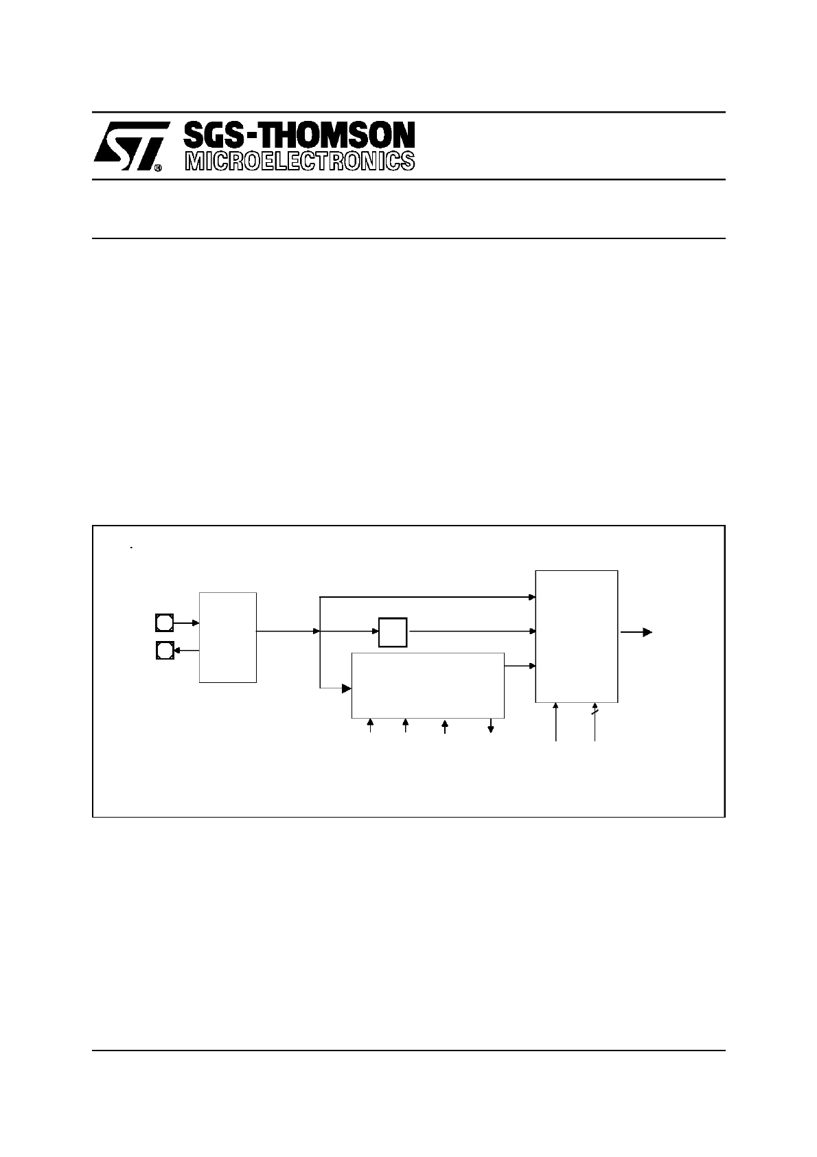
February 1996
1/2
This is advance information from SGS-TH OMSON. Details are subject tochange without notice.
ST10R163
User Manual
14 - SYSTEM CLOCK GENERATOR
The system clock generator includes an on-chip
PLL circuit that allows to operate the ST10R163
on a variety of external clock frequency. This PLL
can multiply the external clock frequency by a
fixed factor of 1.5, 2, 2.5, 3, 4 or 5, this factor is se-
lected via pins P0H.7 through P0H.5 during reset.
The PLL generates a CPU clock signal with 50%
duty cycle. The PLL also provides fail safe mech-
anisms which allow to detect frequency deviations
and to perform emergency actions in case of an
external clock failure. The PLL may also be disa-
bled via pins P0H.7..5 during reset in which case
the ST10R163 will directly run on the external
clock or on external clock divided by 2 (see figure
below).
14.1 PLL Operation
The PLL is enabled when pin P0H.7 is latched
high or low if pin P0H.5 is latched low during reset.
The multiply factor of the PLL is set via pins P0H.6
and P0H.5 latched during reset (see table below).
On power-up, the PLL provides a stable clock sig-
nal on its basic frequency of 2..10 MHz within ca.
0.5 ms after VCC has reached 5 V+/-10%, even if
there is no external clock signal. The PLL starts
synchronizing with the external clock signal as
soon as it is available. Within 2 ms after stable os-
cillations of the external clock within the specified
frequency range, the PLL will be synchronous with
this clock at the frequency (Multiply Factor) *
f
OSC
,
ie. the PLL locks to the external clock.
Figure 11-1. Block Diagram of System Clock Generator
VR02079A
Oscillator
Circuit
: 2
PLL Circuit
f
PLL
= n * f
OSC
n = 1/1.5/2/2.5/3/4/5
MUX
f
CPU
XTAL2
POH. (7..5)
Reset
f
PLL
PWRDN
XP3INT
f
OSC
XTAL1
Reset
POH.(7..5)
Reset
Lock
n
Sleep
3
203
2/2
14 - SYSTEM CLOCK GENERATOR (ST10R163)
System Clock Generator Configuration
Note: If the ST10R163 is required to operate on the desired CPU clock directly after reset, make sure that RSTIN remains
active until the PLL has locked.
The PLL constantly synchronizes to the external
clock signal. Due to the fact that the external fre-
quency is 1/(Multiply Factor)th of the PLL output
frequency, the output frequency may be slightly
higher or lower than the desired frequency. This
jitter is irrelevant for longer time periods. For short
periods (1..4 CPU clock cycles), it remains below
5%.
The PLL detects frequency changes of the input
clock signal and generates an interrupt request in
this case. This warning interrupt indicates that the
PLL frequency is no more locked, ie. no more sta-
ble. This occurs when the input clock is unstable
and especially when the input clock fails complet-
ly, ie. due to a broken crystal. In this case, the syn-
chronization mechanism will reduce the PLL out-
put frequency down to the PLL’s basic frequency
(2..10 MHz). The basic frequency is still generated
and allows the CPU to execute emergency actions
in case of a loss of external clock.
Note: The lock failure interrupt request (XP3IR)
will be generated repeatedly as long as an unsta-
ble (or missing) input clock is detected, even
though XP3IR is cleared upon entry to the inter-
rupt service handler. The software of the lock fail-
ure interrupt service handler should take care of
this fact.
14.2 Prescaler Operation
When pins P0.15-13 (P0H.7-5) equal ’001’ during
reset the CPU clock is derived from the internal
oscillator (input clock signal) by a 2:1 prescaler.
The frequency of f
CPU
is half the frequency of f
X-
TAL
and the high and low time of f
CPU
(ie. the du-
ration of an individual TCL) is defined by the peri-
od of the input clock f
XTAL
.
Note that the PLL is internally running on its free-
running frequency and delivers the clock signal for
the Oscillator Watchdog.
14.3 Direct Drive
When pins P0.15-13 (P0H.7-5) equal ’011’ during
reset the on-chip phase locked loop is disabled
and the CPU clock is directly driven from the inter-
nal oscillator with the input clock signal.
The frequency of f
CPU
directly follows the frequen-
cy of f
XTAL
so the high and low time of f
CPU
(i.e.
the duration of an individual TCL) is defined by the
duty cycle of the input clock f
XTAL
.
Note that the PLL is internally running on its free-
running frequency and delivers the clock signal for
the Oscillator Watchdog.
14.4 Oscillator Watchdog
When the clock option selected is direct drive or
direct drive with prescaler, in order to provide a fail
safe mechanism in case of a loss of the external
clock, an oscillator watchdog is implemented as
an additional functionality of the PLL circuitry. This
oscillator watchdog operates as follows:
After reset, the PLL is running on its free-running
frequency, and increment the Oscillator Watchdog
counter. On each transition of XTAL1 pin, the Os-
cillator Watchdog is cleared. If an external clock
failure occurs, then the Oscillator Watchdog coun-
ter overflows (after 16 PLL clock cycles). The CPU
clock signal will be switched to the PLL free-run-
ning clock signal, and the Oscillator Watchdog In-
terrupt Request (XP3INT) is flagged. The CPU
clock will not switch back to the external clock
even if a valid external clock exits on XTAL1 pin.
Only a hardware reset can switch the CPU clock
source back to direct clock input.
P0H.7
P0H.6
P0H.5
Multiply Factor
1
1
1
f
CPU
= 4 * f
OSC
(default configuration)
1
1
0
f
CPU
= 2 * f
OSC
1
0
1
f
CPU
= 3 * f
OSC
1
0
0
f
CPU
= 5 * f
OSC
0
1
1
f
CPU
= f
OSC
(direct clock drive, PLL is bypassed)
0
1
0
f
CPU
= 1.5 * f
OSC
0
0
1
f
CPU
= 0.5 * f
OSC
(clock prescaler (divider by 2) is enabled, PLL is bypassed)
0
0
0
f
CPU
= 2.5 * f
OSC
204
February 1996
1/12
This is advance information from SGS-TH OMSON. Details are subject tochange without notice.
ST10R163
User Manual
15 - SYSTEM PROGRAMMING
To aid in software development, a number of fea-
tures has been incorporated into the instruction
set of the ST10R163, including constructs for
modularity, loops, and context switching. In many
cases commonly used instruction sequences
have been simplified while providing greater flexi-
bility. The following programming features help to
fully utilize this instruction set.
15.1 INSTRUCTIONS PROVIDED AS SUBSETS
OF INSTRUCTIONS
In many cases, instructions found in other micro-
controllers are provided as subsets of more pow-
erful instructions in the ST10R163. This allows the
same functionality to be provided while decreas-
ing the hardware required and decreasing decode
complexity. In order to aid assembly program-
ming, these instructions, familiar from other micro-
controllers, can be built in macros, thus providing
the same names.
Directly Substitutable Instructions are instruc-
tions known from other microcontrollers that can
be replaced by the following instructions of the
ST10R163:
Modification of System Flags is performed us-
ing bit set or bit clear instructions (BSET, BCLR ).
All bit and word instructions can access the PSW
register, so no instructions like CLEAR CARRY or
ENABLE INTERRUPTS are required.
External Memory Data Access does not require
special instructions to load data pointers or explic-
itly load and store external data. The ST10R163
provides a Von-Neumann memory architecture
and its on-chip hardware automatically detects ac-
cesses to internal RAM, GPRs, and SFRs.
Substituted Instruction
ST10R163 Instruction
Function
CLR
Rn
AND
Rn, #0h
Clear register
CPLB
Bit
BMOVN
Bit, Bit
Complement bit
DEC
Rn
SUB
Rn, #1h
Decrement register
INC
Rn
ADD
Rn, #1h
Increment register
SWAPB
Rn
ROR
Rn, #8h
Swap bytes within word
205

2/12
15 - SYSTEM PROGRAMMING (ST10R163)
15.2 MULTIPLICATION AND DIVISION
Multiplication and division of words and double
words is provided through multiple cycle instruc-
tions implementing a Booth algorithm. Each in-
struction implicitly uses the 32-bit register MD
(MDL = lower 16 bits, MDH = upper 16 bits). The
MDRIU flag (Multiply or Divide Register In Use) in
register MDC is set whenever either half of this
register is written to or when a multiply/divide in-
struction is started. It is cleared whenever the
MDL register is read. Because an interrupt can be
acknowledged before the contents of register MD
are saved, this flag is required to alert interrupt
routines, which require the use of the multiply/di-
vide hardware, so they can preserve register MD.
This register, however, only needs to be saved
when an interrupt routine requires use of the MD
register and a previous task has not saved the cur-
rent result. This flag is easily tested by the Jump-
on-Bit instructions.
Multiplication or division is simply performed by
specifying the correct (signed or unsigned) ver-
sion of the multiply or divide instruction. The result
is then stored in register MD. The overflow flag (V)
is set if the result from a multiply or divide instruc-
tion is greater than 16 bits. This flag can be used
to determine whether both word halves must be
transferred from register MD. The high portion of
register MD (MDH) must be moved into the regis-
ter file or memory first, in order to ensure that the
MDRIU flag reflects the correct state.
The following instruction sequence performs an
unsigned 16 by 16-bit multiplication:
SAVE:
JNB
MDRIU, START
;Test if MD was in use.
SCXT
MDC, #0010H
;Save and clear contro l
;regis ter leaving MDRI U set
;(only required for
;inter rupted multiply/ divi de ;in-
struct ions)
BSET
SAVED
;Indica te the save oper a-
tion
PUSH
MDH
;Save previ ous MD con-
tents. ..
PUSH
MDL
;... on system stack
START:
MULU
R1, R2
;Mul tipl y 16·16 unsigned,
Sets MDRI U
JMPR
cc_NV, COPYL
;Tes t for only 16-bit re-
sult
MOV
R3, MDH
;Mov e high portion of MD
COPYL:
MOV
R4, MDL
;Mov e low port ion of MD,
;Clear s MDRIU
RESTOR E:
JNB
SAVED, DONE
;Tes t if MD registe rs
were ;sav ed
POP
MDL
;Res tore regis ters
POP
MDH
POP
MDC
DONE:
BCLR
SAVED
;Mul tipl icat ion is com-
pleted , ;prog ram continue s
The above save sequence and the restore se-
quence after COPYL are only required if the cur-
rent routine could have interrupted a previous rou-
tine which contained a MUL or DIV instruction.
Register MDC is also saved because it is possible
that a previous routine’s Multiply or Divide instruc-
tion was interrupted while in progress. In this case
the information about how to restart the instruction
is contained in this register. Register MDC must
be cleared to be correctly initialized for a subse-
quent multiplication or division. The old MDC con-
tents must be popped from the stack before the
RETI instruction is executed.
For a division the user must first move the divi-
dend into the MD register. If a 16/16-bit division is
specified, only the low portion of register MD must
be loaded. The result is also stored into register
MD. The low portion (MDL) contains the integer
result of the division, while the high portion (MDH)
contains the remainder.
206

3/12
15 - SYSTEM PROGRAMMING (ST10R163)
MULTIPLICATION AND DIVISION(Cont’d)
The following instruction sequence performs a 32
by 16-bit division:
MOV
MDH, R1
;Move divid end to MD regis ter.
;Sets MDRIU
MOV
MDL, R2
;Move low portio n to MD
DIV
R3
;Divide 32/16 signed , R3 holds the
;diviso r
JMPR
cc_V, ERROR
;Test for divide overflow
MOV
R3, MDH
;Move remai nder to R3
MOV
R4, MDL
;Move integer result to R4. Clears
;MDRIU
Whenever a multiply or divide instruction is inter-
rupted while in progress, the address of the inter-
rupted instruction is pushed onto the stack and the
MULIP flag in the PSW of the interrupting routine
is set. When the interrupt routine is exited with the
RETI instruction, this bit is implicitly tested before
the old PSW is popped from the stack. If
MULIP=’1’ the multiply/divide instruction is re-read
from the location popped from the stack (return
address) and will be completed after the RETI in-
struction has been executed.
Note: The MULIP flag is part of thecontext of the
interrupted task. When the interrupting routine
does not return to the interrupted task (eg. sched-
uler switches to another task) the MULIP flag must
be set or cleared according to the context of the
task that is switched to.
15.3 BCD CALCULATIONS
No direct support for BCD calculations is provided
in the ST10R163. BCD calculations are performed
by converting BCD data to binary data, performing
the desired calculations using standard data
types, and converting the result back to BCD data.
Due to the enhanced performance of division in-
structions binary data is quickly converted to BCD
data through division by 10d. Conversion from
BCD data to binary data is enhanced by multiple
bit shift instructions. This provides similar perform-
ance compared to instructions directly supporting
BCD data types, while no additional hardware is
required.
15.4 STACK OPERATIONS
The ST10R163 supports two types of stacks. The
system stack is used implicitly by the controller
and is located in the internal RAM. The user stack
provides stack access to the user in either the in-
ternal or external memory. Both stack types grow
from high memory addresses to low memory ad-
dresses.
Internal System Stack
A system stack is provided to store return vectors,
segment pointers, and processor status for proce-
dures and interrupt routines. A system register,
SP, points to the top of the stack. This pointer is
decremented when data is pushed onto the stack,
and incremented when data is popped.
The internal system stack can also be used to
temporarily store data or pass it between subrou-
tines or tasks. Instructions are provided to push or
pop registers on/from the system stack. However,
in most cases the register banking scheme pro-
vides the best performance for passing data be-
tween multiple tasks.
Note: The system stack allows to store words on-
ly. Bytes must either be converted to words or the
respective other byte must be disregarded.
Register SP can only be loaded with even byte ad-
dresses (The LSB of SP is always ’0’).
207

4/12
15 - SYSTEM PROGRAMMING (ST10R163)
STACK OPERATIONS (Cont’d)
Detection of stack overflow/underflow is support-
ed by two registers, STKOV (Stack Overflow
Pointer) and STKUN (Stack Underflow Pointer).
Specific system traps (Stack Overflow trap, Stack
Underflow trap) will be entered whenever the SP
reaches either boundary specified in these regis-
ters.
The contents of the stack pointer are compared to
the contents of the overflow register, whenever
the SP is DECREMENTED either by a CALL,
PUSH or SUB instruction. An overflow trap will be
entered, when the SP value is less than the value
in the stack overflow register.
The contents of the stack pointer are compared to
the contents of the underflow register, whenever
the SP is INCREMENTED either by a RET, POP
or ADD instruction. An underflow trap will be en-
tered, when the SP value is greater than the value
in the stack underflow register.
Note: When a value is MOVED into the stack
pointer, NO check against the overflow/underflow
registers is performed.
In many cases the user will place a software reset
instruction (SRST) into the stack underflow and
overflow trap service routines. This is an easy ap-
proach, which does not require special program-
ming. However, this approach assumes that the
defined internal stack is sufficient for the current
software and that exceeding its upper or lower
boundary represents a fatal error.
It is also possible to use the stack underflow and
stack overflow traps to cache portions of a larger
external stack. Only the portion of the system
stack currently being used is placed into the inter-
nal memory, thus allowing a greater portion of the
internal RAM to be used for program, data or reg-
ister banking. This approach assumes no error but
requires a set of control routines (see below).
Circular (virtual) Stack
This basic technique allows data to be pushed un-
til the overflow boundary of the internal stack is
reached. At this point a portion of the stacked data
must be saved into external memory to create
space for further stack pushes. This is called
“stack flushing”. When executing a number of re-
turn or pop instructions, the upper boundary (since
the stack empties upward to higher memory loca-
tions) is reached. The entries that have been pre-
viously saved in external memory must now be re-
stored. This is called “stack filling”. Because pro-
cedure call instructions do not continue to nest in-
finitely and call and return instructions alternate,
flushing and filling normally occurs very infre-
quently. If this is not true for a given program envi-
ronment, this technique should not be used be-
cause of the overhead of flushing and filling.
The basic mechanism is the transformation of
the addresses of a virtual stack area, controlled
via registers SP, STKOV and STKUN, to a defined
physical stack area within the internal RAM via
hardware. This virtual stack area covers all possi-
ble locations that SP can point to, ie. 00’F000h
through 00’FFFEh. STKOV and STKUN accept
the same 4 KByte address range.
The size of the physical stack area within the inter-
nal RAM that effectively is used for standard stack
operations is defined via bitfield STKSZ in register
SYSCON (see below).
The virtual stack addresses are transformed to
physical stack addresses by concatenating the
significant bits of the stack pointer register SP
(see table) with the complementary most signifi-
cant bits of the upper limit of the physical stack
area (00’FBFEh). This transformation is done via
hardware (see figure below).
The
reset
values
(STKOV=FA00h,
STKUN=FC00h, SP=FC00h, STKSZ=000b) map
the virtual stack area directly to the physical stack
area and allow to use internal system stack with-
out any changes, provided that the 256 word area
is not exceeded.
<STKSZ>
Stack Size
(Words)
Internal RAM Addresses (Words)
of Physical Stack
Significant Bits of
Stack Point er SP
0 0 0 b
256
00’FBFEh...00’FA00h (Default after Reset)
SP.8...SP.0
0 0 1 b
128
00’FBFEh...00’FB00h
SP.7...SP.0
0 1 0 b
64
00’FBFEh...00’FB80h
SP.6...SP.0
0 1 1 b
32
00’FBFEh...00’FBC0h
SP.5...SP.0
1 0 0 b
---
Reserved. Do not use this combination.
---
1 0 1 b
---
Reserved. Do not use this combination.
---
1 1 0 b
---
Reserved. Do not use this combination.
---
1 1 1 b
1024
00’FDFEh...00’F600h (Note: No circular stack)
SP.11...SP.0
208
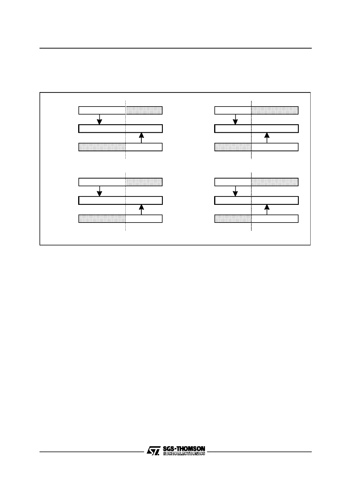
5/12
15 - SYSTEM PROGRAMMING (ST10R163)
STACK OPERATIONS (Cont’d)
Figure 12-1. Physical Stack Address Generation
The following example demonstrates the circular
stack mechanism which is also an effect of this vir-
tual stack mapping: First, register R1 is pushed
onto the lowest physical stack location according
to the selected maximum stack size. With the fol-
lowing instruction, register R2 will be pushed onto
the highest physical stack location although the
SP is decremented by 2 as for the previous push
operation.
MOV SP, #0F8 02h
;Set SP befo re last entry of
;physic al stack of 256 words
...
;(SP) =
F802h: Physi cal stack
;addres s = FA02h
PUSH R1
;(SP) =
F800h: Physi cal stack
;addres s = FA00h
PUSH R2
;(SP) =
F7FEh: Physic al stack
;addres s = FBFEh
The effect of the address transformation is that the
physical stack addresses wrap around from the
end of the defined area to its beginning. When
flushing and filling the internal stack, this circular
stack mechanism only requires to move that por-
tion of stack data which is really to be re-used (ie.
the upper part of the defined stack area) instead of
the whole stack area. Stack data that remain in the
lower part of the internal stack need not be moved
by the distance of the space being flushed or filled,
as the stack pointer automatically wraps around to
the beginning of the freed part of the stack area.
Note: This circular stack technique is applicable
for stack sizes of 32 to 256 words (STKSZ = ‘000b’
to ‘0116b’), it does not work with option STKSZ =
‘111b’, which uses the complete internal RAM for
system stack.
When a boundary is reached, the stack underflow
or overflow trap is entered, where the user moves
a predetermined portion of the internal stack to or
from the external stack. The amount of data trans-
ferred is determined by the average stack space
required by routines and the frequency of calls,
traps, interrupts and returns. In most cases this
will be approximately one quarter to one tenth the
size of the internal stack. Once the transfer is
complete, the boundary pointers are updated to
reflect the newly allocated space on the internal
stack. Thus, the user is free to write code without
concern for the internal stack limits. Only the exe-
cution time required by the trap routines affects
user programs.
1 1 1 1 1 0 1 1 1 1 1 1 1 1 1 0
1 1 1 1 1 0 1 1 1 0 0 0 0 0 0 0
1 1 1 1 1 0 1 1 1 0 0 0 0 0 0 0
1 1 1 1 1 0 1 0 0 0 0 0 0 0 0 0
1 1 1 1 1 0 1 1 1 1 1 1 1 1 1 0
1 1 1 1 1 0 1 1 0 1 1 1 1 1 1 0
1 1 1 1 1 0 1 1 1 1 1 1 1 1 1 0
FBFEh
FB80h
FB80h
FBFEh
FB7Eh
FBFEh
FBFEh
64 words
256 words
F800h 1 1 1 1 1 0 0 0 0 0 0 0 0 0 0 0
FA00h
1 1 1 1 0 1 1 1 1 1 1 1 1 1 1 0
1 1 1 1 1 0 1 1 1 1 1 1 1 1 1 0
FBFEh
F7FEh
FBFEh
1 1 1 1 1 0 1 1 1 1 1 1 1 1 1 0
1 1 1 1 1 0 1 1 1 1 1 1 1 1 1 0
<SP>
<SP>
Phys.A.
Phys.A.
Stack Size
After PUSH
After PUSH
209

6/12
15 - SYSTEM PROGRAMMING (ST10R163)
STACK OPERATIONS (Cont’d)
The following procedure initializes the controller
for usage of the circular stack mechanism:
•
Specify the size of the physical system stack
area within the internal RAM (bitfield STKSZ in
register SYSCON).
•
Define two pointers, which specify the upper and
lower boundary of the external stack. These val-
ues are then tested in the stack underflow and
overflow trap routines when moving data.
•
Set the stack overflow pointer (STKOV) to the
limit of the defined internal stack area plus six
words (for the reserved space to store two inter-
rupt entries).
The internal stack will now fill until the overflow
pointer is reached. After entry into the overflow
trap procedure, the top of the stack will be copied
to the external memory. The internal pointers will
then be modified to reflect the newly allocated
space. After exiting from the trap procedure, the
internal stack will wrap around to the top of the in-
ternal stack, and continue to grow until the new
value of the stack overflow pointer is reached.
When the underflow pointer is reached while the
stack is emptied the bottom of stack is reloaded
from the external memory and the internal point-
ers are adjusted accordingly.
Linear Stack
The ST10R163 also offers a linear stack option
(STKSZ = ‘111b’), where the system stack may
use the complete internal RAM area. This allows
to provide a large system stack without requiring
procedures to handle data transfers for a circular
stack. However, this method also leaves less
RAM space for variables or code. The RAM area
that may effectively be consumed by the system
stack is defined via the STKUN and STKOV point-
ers. The underflow and overflow traps in this case
serve for fatal error detection only.
For the linear stack option all modifiable bits of
register SP are used to access the physical stack.
Although the stack pointer may cover addresses
from 00’F000h up to 00’FFFEh the (physical) sys-
tem stack must be located within the internal RAM
and therefore may only use the address range
00’F600h to 00’FDFEh. It is the user’s responsibil-
ity to restrict the system stack to the internal RAM
range.
Note: Avoid stack accesses within address range
00’F000h to 00’F5FEh (ESFR space and reserved
area) and within address range 00’FE00h and
00’FFFEh (SFR space). Otherwise unpredictable
results will occur.
User Stacks
User stacks provide the ability to create task spe-
cific data stacks and to off-load data from the sys-
tem stack. The user may push both bytes and
words onto a user stack, but is responsible for us-
ing the appropriate instructions when popping
data from the specific user stack. No hardware de-
tection of overflow or underflow of a user stack is
provided. The following addressing modes allow
implementation of user stacks:
[– Rw], Rb or [– Rw], Rw: Pre-decrement Indirect
Addressing.
Used to push one byte or word onto a user stack.
This mode is only available for MOV instructions
and can specify any GPR as the user stack point-
er.
Rb, [Rw+] or Rw, [Rw+]: Post-increment Index
Register Indirect Addressing.
Used to pop one byte or word from a user stack.
This mode is available to most instructions, but
only GPRs R0-R3 can be specified as the user
stack pointer.
Rb, [Rw+] or Rw, [Rw+]: Post-increment Indirect
Addressing.
Used to pop one byte or word from a user stack.
This mode is only available for MOV instructions
and can specify any GPR as the user stack point-
er.
15.5 REGISTER BANKING
Register banking provides the user with an ex-
tremely fast method to switch user context. A sin-
gle machine cycle instruction saves the old bank
and enters a new register bank. Each register
bank may assign up to 16 registers. Each register
bank should be allocated during coding based on
the needs of each task. Once the internal memory
has been partitioned into a register bank space,
internal stack space and a global internal memory
area, each bank pointer is then assigned. Thus,
upon entry into a new task, the appropriate bank
pointer is used as the operand for the SCXT
(switch context) instruction. Upon exit from a task
a simple POP instruction to the context pointer
(CP) restores the previous task’s register bank.
210

7/12
15 - SYSTEM PROGRAMMING (ST10R163)
15.6 PROCEDURE CALL ENTRY AND EXIT
To support modular programming a procedure
mechanism is provided to allow coding of fre-
quently used portions of code into subroutines.
The CALL and RET instructions store and restore
the value of the instruction pointer (IP) on the sys-
tem stack before and after a subroutine is execut-
ed.
Note: Procedures may be called conditionally with
instructions CALLA or CALLI, or be called uncon-
ditionally using instructions CALLR or CALLS.
Any data pushed onto the system stack during ex-
ecution of the subroutine must be popped before
the RET instruction is executed.
Passing Parameters on the System Stack
Parameters may be passed via the system stack
through PUSH instructions before the subroutine
is called, and POP instructions during execution of
the subroutine. Base plus offset indirect address-
ing also permits access to parameters without
popping these parameters from the stack during
execution of the subroutine. Indirect addressing
provides a mechanism of accessing data refer-
enced by data pointers, which are passed to the
subroutine.
In addition, two instructions have been implement-
ed to allow one parameter to be passed on the
system stack without additional software over-
head.
The PCALL (push and call) instruction first pushes
the ’reg’ operand and the IP contents onto the sys-
tem stack and then passes control to the subrou-
tine specified by the ’caddr’ operand.
When exiting from the subroutine, the RETP (re-
turn and pop) instruction first pops the IP and then
the ’reg’ operand from the system stack and re-
turns to the calling program.
Cross Segment Subroutine Calls
Calls to subroutines in different segments require
the use of the CALLS (call inter-segment subrou-
tine) instruction. This instruction preserves both
the CSP (code segment pointer) and IP on the
system stack.
Upon return from the subroutine, a RETS (return
from inter-segment subroutine) instruction must
be used to restore both the CSP and IP. This en-
sures that the next instruction after the CALLS in-
struction is fetched from the correct segment.
Note: It is possible to use CALLS within the same
segment, but still two words of the stack are used
to store both the IP and CSP.
Providing Local Registers for Subroutines
For subroutines which require local storage, the
following methods are provided:
Alternate Bank of Registers: Upon entry into a
subroutine, it is possible to specify a new set of lo-
cal registers by executing the SCXT (switch con-
text) instruction. This mechanism does not provide
a method to recursively call a subroutine.
Saving and Restoring of Registers: To provide
local registers, the contents of the registers which
are required for use by the subroutine can be
pushed onto the stack and the previous values be
popped before returning to the calling routine. This
is the most common technique used today and it
does provide a mechanism to support recursive
procedures. This method, however, requires two
machine cycles per register stored on the system
stack (one cycle to PUSH the register, and one to
POP the register).
211
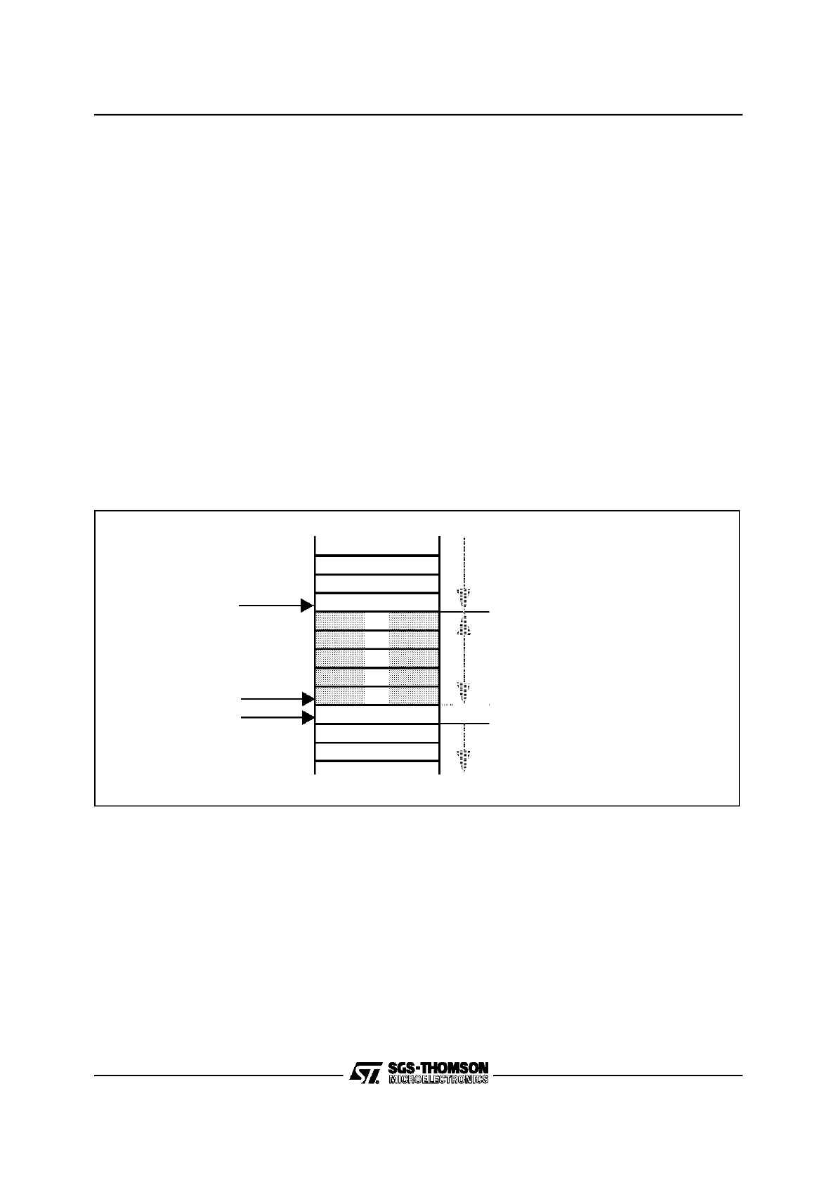
8/12
15 - SYSTEM PROGRAMMING (ST10R163)
PROCEDURE CALL ENTRY AND EXIT(Cont’d)
Use of the System Stack for LocalRegisters: It
is possible to use the SP and CP to set up local
subroutine register frames. This allows subrou-
tines to dynamically allocate local variables as
needed within two machine cycles. A local frame
is allocated by simply subtracting the number of
required local registers from the SP, and then
moving the value of the new SP to the CP.
This operation is supported through the SCXT
(switch context) instruction with the addressing
mode ’reg, mem’. Using this instruction saves the
old contents of the CP on the system stack and
moves the value of the SP into CP (see example
below). Each local register is then accessed as if it
was a normal register. Upon exit from the subrou-
tine, first the old CP must be restored by popping it
from the stack and then the number of used local
registers must be added to the SP to restore the
allocated local space back to the system stack.
Note: The system stack is growing downwards,
while the register bank is growing upwards.
The software to provide the local register bank for
the example above is very compact:
After entering the subroutine:
SUB
SP, #10
;Free 5 word s in the curren t system
;stack
SCXT
CP, SP
;Set the new registe r bank poin ter
Before exiting the subroutine:
POP
CP
;Resto re the old regis ter bank
ADD
SP, #10
;Relea se the 5 word of the current
;syste m stack
Figure 12-2. Local Registers
Old
Stack
Area
Newly
Allocated
Register
Bank
R4
R3
R2
R1
R0
Old CP Contents
Old SP
New SP
New CP
New
Stack
Area
212

9/12
15 - SYSTEM PROGRAMMING (ST10R163)
15.7 TABLE SEARCHING
A number of features have been included to de-
crease the execution time required to search ta-
bles. First, branch delays are eliminated by the
branch target cache after the first iteration of the
loop. Second, in non-sequentially searched ta-
bles, the enhanced performance of the ALU al-
lows more complicated hash algorithms to be
processed to obtain better table distribution. For
sequentially searched tables, the auto-increment
indirect addressing mode and the E (end of table)
flag stored in the PSW decrease the number of
overhead instructions executed in the loop.
The two examples below illustrate searching or-
dered tables and non-ordered tables, respectively:
MOV
R0, #BASE
;Move tabl e base into R0
LOOP:
CMPR1, [R0+
;Compare targe t to table entry
JMPR
cc_SGT, LOO
;Test whet her target has not been
;found
Note: The last entry in the table must be greater
than the largest possible target.
MOV
R0, #BASE
;Move tabl e base into R0
LOOP:
CMPR1, [R0+]
;Compare targe t to table entry
JMPR
cc_NET, LOO
;Test whet her target is not found
;AND the end of table...
;...has not been reached .
Note: The last entry in the table must be equal to
the lowest signed integer (8000h).
15.8
PERIPHERAL
CONTROL
AND
INTERFACE
All communication between peripherals and the
CPU is performed either by PEC transfers to and
from internal memory, or by explicitly addressing
the SFRs associated with the specific peripherals.
After resetting the ST10R163 all peripherals (ex-
cept the watchdog timer) are disabled and initial-
ized to default values. A desired configuration of a
specific peripheral is programmed using MOV in-
structions of either constants or memory values to
specific SFRs. Specific control flags may also be
altered via bit instructions.
Once in operation, the peripheral operates auton-
omously until an end condition is reached at which
time it requests a PEC transfer or requests CPU
servicing through an interrupt routine. Information
may also be polled from peripherals through read
accesses to SFRs or bit operations including
branch tests on specific control bits in SFRs. To
ensure proper allocation of peripherals among
multiple tasks, a portion of the internal memory
has been made bit addressable to allow user sem-
aphores. Instructions have also been provided to
lock out tasks via software by setting or clearing
user specific bits and conditionally branching
based on these specific bits.
It is recommended that bit fields in control SFRs
are updated using the BFLDH and BFLDL instruc-
tions or a MOV instruction to avoid undesired in-
termediate modes of operation which can occur,
when BCLR/BSET or AND/OR instruction se-
quences are used.
15.9 FLOATING POINT SUPPORT
All floating point operations are performed using
software. Standard multiple precision instructions
are used to perform calculations on data types
that exceed the size of the ALU. Multiple bit rotate
and logic instructions allow easy masking and ex-
tracting of portions of floating point numbers.
To decrease the time required to perform floating
point operations, two hardware features have
been implemented in the CPU core. First, the PRI-
OR instruction aids in normalizing floating point
numbers by indicating the position of the first set
bit in a GPR. This result can the be used to rotate
the floating point result accordingly. The second
feature aids in properly rounding the result of nor-
malized floating point numbers through the over-
flow (V) flag in the PSW. This flag is set when a
one is shifted out of the carry bit during shift right
operations. The overflow flag and the carry flag
are then used to round the floating point result
based on the desired rounding algorithm.
15.10 TRAP/INTERRUPT ENTRY AND EXIT
Interrupt routines are entered when a requesting
interrupt has a priority higher than the current CPU
priority level. Traps are entered regardless of the
current CPU priority. When either a trap or inter-
rupt routine is entered, the state of the machine is
preserved on the system stack and a branch to the
appropriate trap/interrupt vector is made.
All trap and interrupt routines require the use of
the RETI (return from interrupt) instruction to exit
from the called routine. This instruction restores
the system state from the system stack and then
branches back to the location where the trap or in-
terrupt occurred.
213

10/12
15 - SYSTEM PROGRAMMING (ST10R163)
15.11
UNSEPARABLE
INSTRUCTION
SEQUENCES
The instructions of the ST10R163 are very effi-
cient (most instructions execute in one machine
cycle) and even the multiplication and division are
interruptable in order to minimize the response la-
tency to interrupt requests (internal and external).
In many microcontroller applications this is vital.
Some special occasions, however, require certain
code sequences (eg. semaphore handling) to be
uninterruptable to function properly. This can be
provided by inhibiting interrupts during the respec-
tive code sequence by disabling and enabling
them before and after the sequence. The neces-
sary overhead may be reduced by means of the
ATOMIC instruction, which allows to lock 1...4 in-
structions to an unseparable code sequence, dur-
ing which the interrupt system (standard interrupts
and PEC requests) and Class A Traps (NMI,
stack overflow/underflow) are disabled. AClass B
Trap (illegal opcode, illegal bus access, etc.),
however, will interrupt the atomic sequence, since
it indicates a severe hardware problem. The inter-
rupt inhibit caused by an ATOMIC instruction gets
active immediately, ie. no other instruction will en-
ter the pipeline except the one that follows the
ATOMIC instruction, and no interrupt request will
be serviced in between. All instructions requiring
multiple cycles or hold states are regarded as one
instruction in this sense (eg. MUL is one instruc-
tion). Any instruction type can be used within an
unseparable code sequence.
EXAMPLE:
ATOMIC #3
The follow ing 3 inst ruct ions are
locked (No NOP requi red)
MOV
R0, #1234h
;Instru ction 1 (no other instr .
;enters the pipel ine! )
MOV
R1, #5678h
;Instruc tion 2
MUL
R0, R1
;Instruc tion 3: MUL regarde d as one
;instruc tion
MOV
R2, MDL
;This inst ruct ion is out of the
;scope of the ATOMIC instructio n
;sequenc e
15.12 OVERRIDING THE DPP ADDRESSING
MECHANISM
The standard mechanism to access data locations
uses one of the four data page pointers (DPPx),
which selects a 16 KByte data page, and a 14-bit
offset within this data page. The four DPPs allow
immediate access to up to 64 KByte of data. In ap-
plications with big data arrays, especially in HLL
applications using large memory models, this may
require frequent reloading of the DPPs, even for
single accesses.
The EXTP (extend page) instruction allows to
switch to an arbitrary data page for 1...4 instruc-
tions without having to change the current DPPs.
EXAMPLE:
EXTP
R15, #1
;The over ride page number is stored
;in R15
MOV
R0, [R14]
;The (14- bit) page offset is stored
;in R14
MOV
R1, [R13]
;This instructio n uses the stan dard
;DPP sche me!
The EXTS (extend segment) instructionallows
to switch to a 64 KByte segment oriented data ac-
cess scheme for 1...4 instructions without having
to change the current DPPs. In this case all 16 bits
of the operand address are used as segment off-
set, with the segment taken from the EXTS in-
struction. This greatly simplifies address calcula-
tion with continuous data like huge arrays in “C”.
EXAMPLE
EXTS
#15, #1
;The over ride seg. is #15
;(0F’0 000h...0F’F FFFh)
MOV
R0, [R14]
;The (16- bit) segment offs et is
;store d in R14
MOV
R1, [R13]
;This instructio n uses the stan dard
;DPP sche me!
214

11/12
15 - SYSTEM PROGRAMMING (ST10R163)
OVERRIDING THE DPP ADDRESSING MECHANISM(Cont’d)
Note: Instructions EXTP and EXTS inhibit inter-
rupts the same way as ATOMIC.
Short Addressing in the Extended SFR (ESFR)
Space
The short addressing modes of the ST10R163
(REG or BITOFF) implicitly access the SFR
space. The additional ESFR space would have to
be accessed via long addressing modes (MEM or
[Rw]). The EXTR (extend register) instruction al-
lows to redirect accesses in short addressing
modes to the ESFR space for 1...4 instructions, so
the additional registers can be accessed this way,
too.
The EXTPR and EXTSR instructions combine the
DPP override mechanism with the redirection to
the ESFR space using a single instruction.
Note: Instructions EXTR, EXTPR and EXTSR in-
hibit interrupts the same way as ATOMIC.
The switching to the ESFR area and data page
overriding is checked by the development tools or
handled automatically.
Nested Locked Sequences
Each of the described extension instruction and
the ATOMIC instruction starts an internal “exten-
sion counter” counting the effected instructions.
When another extension or ATOMIC instruction is
contained in the current locked sequence this
counter is restarted with the value of the new in-
struction. This allows to construct locked sequenc-
es longer than 4 instructions.
Note:
– Interrupt latencies may be increased when
using locked code sequences.
– PEC requests are not serviced during idle
mode, if the IDLE instruction is part of a
locked sequence.
215

12/12
15 - SYSTEM PROGRAMMING (ST10R163)
Notes:
216
February 1996
1/10
This is advance information from SGS-TH OMSON. Details are subject tochange without notice.
ST10R163
User Manual
16 - REGISTER SET
This section summarizes all registers, which are
implemented in the ST10R163 and explains the
description format which is used in the chapters
describing the function and layout of the SFRs.
For easy reference the registers are ordered ac-
cording to two different keys (except for GPRs):
•
Ordered by address, to check which register a
given address references,
•
Ordered by register name, to find the location of
a specific register.
Register Description Format
In the respective chapters the function and the lay-
out of the SFRs is described in a specific format
which provides a number of details about the de-
scribed special function register. The example be-
low shows how to interpret these details.
A word register looks like this:
Elements:
REG_NAMEName of this register
A16 / A8Long 16-bit address / Short 8-bit address
E/SFRRegister space (SFR or ESFR)
(* *) * *Register contents after reset
0/1: defined value, X: undefined, U: un-
changed (undefined after power up)
hwbitBits that are set/cleared by hardware are
marked with a shaded access box
REG_NAME (A16h / A8h)
E/SFR
Reset Value: * * * *h
A byte register looks like this:
REG_NAME (A16h / A8h)
E/SFR
Reset Value: - - * *h
Bit
Functio n
bit(field)name
Explanation of bit(field)name
Description of the functions controlled by this bit(field).
5
4
3
2
1
0
11
10
9
8
7
6
15
14
13
12
rw
rw
-
w
rw
r
rw
rw
-
-
-
-
res.
res.
res.
res.
res.
write
only
read
only
bitfield
bitfi eld
hw
bit
std
bit
hw
bit
5
4
3
2
1
0
11
10
9
8
7
6
15
14
13
12
rw
rw
-
-
-
-
rw
rw
-
-
-
-
bitfield
bitfield
std
bit
hw
bit
217

2/10
16 - REGISTER SET (ST10R163)
16.1 CPU GENERAL PURPOSE REGISTERS (GPRS)
The GPRs form the register bank that the CPU
works with. This register bank may be located an-
ywhere within the internal RAM via the Context
Pointer (CP). Due to the addressing mechanism,
GPR banks can only reside within the internal
RAM. All GPRs are bit-addressable.
Name
Physical
Address
8-Bit
Address
Description
Reset
Value
R0
(CP) + 0
F0h
CPU General Purpose (Word) Register R0
UUUUh
R1
(CP) + 2
F1h
CPU General Purpose (Word) Register R1
UUUUh
R2
(CP) + 4
F2h
CPU General Purpose (Word) Register R2
UUUUh
R3
(CP) + 6
F3h
CPU General Purpose (Word) Register R3
UUUUh
R4
(CP) + 8
F4h
CPU General Purpose (Word) Register R4
UUUUh
R5
(CP) + 10
F5h
CPU General Purpose (Word) Register R5
UUUUh
R6
(CP) + 12
F6h
CPU General Purpose (Word) Register R6
UUUUh
R7
(CP) + 14
F7h
CPU General Purpose (Word) Register R7
UUUUh
R8
(CP) + 16
F8h
CPU General Purpose (Word) Register R8
UUUUh
R9
(CP) + 18
F9h
CPU General Purpose (Word) Register R9
UUUUh
R10
(CP) + 20
FAh
CPU General Purpose (Word) Register R10
UUUUh
R11
(CP) + 22
FBh
CPU General Purpose (Word) Register R11
UUUUh
R12
(CP) + 24
FCh
CPU General Purpose (Word) Register R12
UUUUh
R13
(CP) + 26
FDh
CPU General Purpose (Word) Register R13
UUUUh
R14
(CP) + 28
FEh
CPU General Purpose (Word) Register R14
UUUUh
R15
(CP) + 30
FFh
CPU General Purpose (Word) Register R15
UUUUh
218

3/10
16 - REGISTER SET (ST10R163)
CPU GENERAL PURPOSE REGISTERS (GPRS)(Cont’d)
The first 8 GPRs (R7...R0) may also be accessed
bytewise. Other than with SFRs, writing to a GPR
byte does not affect the other byte of the respec-
tive GPR.
The respective halves of the byte-accessible reg-
isters receive special names:
Name
Physical
Address
8-Bit
Address
Description
Reset
Value
RL0
(CP) + 0
F0h
CPU General Purpose (Byte) Register RL0
UUh
RH0
(CP) + 1
F1h
CPU General Purpose (Byte) Register Rh0
UUh
RL1
(CP) + 2
F2h
CPU General Purpose (Byte) Register RL1
UUh
RH1
(CP) + 3
F3h
CPU General Purpose (Byte) Register RH1
UUh
RL2
(CP) + 4
F4h
CPU General Purpose (Byte) Register RL2
UUh
RH2
(CP) + 5
F5h
CPU General Purpose (Byte) Register RH2
UUh
RL3
(CP) + 6
F6h
CPU General Purpose (Byte) Register RL3
UUh
RH3
(CP) + 7
F7h
CPU General Purpose (Byte) Register RH3
UUh
RL4
(CP) + 8
F8h
CPU General Purpose (Byte) Register RL4
UUh
RH4
(CP) + 9
F9h
CPU General Purpose (Byte) Register RH4
UUh
RL5
(CP) + 10
FAh
CPU General Purpose (Byte) Register RL5
UUh
RH5
(CP) + 11
FBh
CPU General Purpose (Byte) Register RH5
UUh
RL6
(CP) + 12
FCh
CPU General Purpose (Byte) Register RL6
UUh
RH6
(CP) + 13
FDh
CPU General Purpose (Byte) Register RH6
UUh
RL7
(CP) + 14
FEh
CPU General Purpose (Byte) Register RL7
UUh
RH7
(CP) + 14
FFh
CPU General Purpose (Byte) Register RH7
UUh
219

4/10
16 - REGISTER SET (ST10R163)
16.2 SPECIAL FUNCTION REGISTERS ORDERED BY NAME
The following table lists all SFRs which are imple-
mented in the ST10R163 in alphabetical order.
Bit-addressable SFRs are marked with the letter
“b” in column “Name”. SFRs within the Extended
SFR-Space (ESFRs) are marked with the letter
“E” in column “Physical Address”.
Name
Physical
Address
8-Bit
Address
Description
Reset
Value
ADDRSEL1
FE18h
0Ch
Address Select Register 1
0000h
ADDRSEL2
FE1Ah
0Dh
Address Select Register 2
0000h
ADDRSEL3
FE1Ch
0Eh
Address Select Register 3
0000h
ADDRSEL4
FE1Eh
0Fh
Address Select Register 4
0000h
BUSCON0
b
FF0Ch
86h
Bus Configuration Register 0
0000h
BUSCON1
b
FF14h
8Ah
Bus Configuration Register 1
0000h
BUSCON2
b
FF16h
8Bh
Bus Configuration Register 2
0000h
BUSCON3
b
FF18h
8Ch
Bus Configuration Register 3
0000h
BUSCON4
b
FF1Ah
8Dh
Bus Configuration Register 4
0000h
CAPREL
FE4Ah
25h
GPT2 Capture/Reload Register
0000h
CC8IC
b
FF88h
C4h
External Interrupt 0 Control Register
0000h
CC9IC
b
FF8Ah
C5h
External Interrupt 1 Control Register
0000h
CC10IC
b
FF8Ch
C6h
External Interrupt 2 Control Register
0000h
CC11IC
b
FF8Eh
C7h
External Interrupt 3 Control Register
0000h
CC12IC
b
FF90h
C8h
External Interrupt 4 Control Register
0000h
CC13IC
b
FF92h
C9h
External Interrupt 5 Control Register
0000h
CC14IC
b
FF94h
CAh
External Interrupt 6 Control Register
0000h
CC15IC
b
FF96h
CBh
External Interrupt 7 Control Register
0000h
CP
FE10h
08h
CPU Context Pointer Register
FC00h
CRIC
b
FF6Ah
B5h
GPT2 CAPREL Interrupt Control Register
0000h
CSP
FE08h
04h
CPU Code Segment Pointer Register
(8 bits, not directly writeable)
0000h
DP0L
b
F100h E
80h
P0L Direction Control Register
00h
DP0H
b
F102h E
81h
P0H Direction Control Register
00h
DP1L
b
F104h E
82h
P1L Direction Control Register
00h
DP1H
b
F106h E
83h
P1H Direction Control Register
00h
DP2
b
FFC2h
E1h
Port 2 Direction Control Register
0000h
DP3
b
FFC6h
E3h
Port 3 Direction Control Register
0000h
DP4
b
FFCAh
E5h
Port 4 Direction Control Register
00h
DP6
b
FFCEh
E7h
Port 6 Direction Control Register
00h
DPP0
FE00h
00h
CPU Data Page Pointer 0 Register (10 bits)
0000h
DPP1
FE02h
01h
CPU Data Page Pointer 1 Register (10 bits)
0001h
DPP2
FE04h
02h
CPU Data Page Pointer 2 Register (10 bits)
0002h
DPP3
FE06h
03h
CPU Data Page Pointer 3 Register (10 bits)
0003h
EXICON
b
F1C0h E
E0h
External Interrupt Control Register
0000h
220

5/10
16 - REGISTER SET (ST10R163)
MDC
b
FF0Eh
87h
CPU Multiply Divide Control Register
0000h
MDH
FE0Ch
06h
CPU Multiply Divide Register – High Word
0000h
MDL
FE0Eh
07h
CPU Multiply Divide Register – Low Word
0000h
ODP2
b
F1C2h E
E1h
Port 2 Open Drain Control Register
0000h
ODP3
b
F1C6h E
E3h
Port 3 Open Drain Control Register
0000h
ODP6
b
F1CEh E
E7h
Port 6 Open Drain Control Register
00h
ONES
b
FF1Eh
8Fh
Constant Value 1’s Register (read only)
FFFFh
P0L
b
FF00h
80h
Port 0 Low Register (Lower half of PORT0)
00h
P0H
b
FF02h
81h
Port 0 High Register (Upper half of PORT0)
00h
P1L
b
FF04h
82h
Port 1 Low Register (Lower half of PORT1)
00h
P1H
b
FF06h
83h
Port 1 High Register (Upper half of PORT1)
00h
P2
b
FFC0h
E0h
Port 2 Register
0000h
P3
b
FFC4h
E2h
Port 3 Register
0000h
P4
b
FFC8h
E4h
Port 4 Register (8 bits)
00h
P5
b
FFA2h
D1h
Port 5 Register (read only)
XXXXh
P6
b
FFCCh
E6h
Port 6 Register (8 bits)
00h
PECC0
FEC0h
60h
PEC Channel 0 Control Register
0000h
PECC1
FEC2h
61h
PEC Channel 1 Control Register
0000h
PECC2
FEC4h
62h
PEC Channel 2 Control Register
0000h
PECC3
FEC6h
63h
PEC Channel 3 Control Register
0000h
PECC4
FEC8h
64h
PEC Channel 4 Control Register
0000h
PECC5
FECAh
65h
PEC Channel 5 Control Register
0000h
PECC6
FECCh
66h
PEC Channel 6 Control Register
0000h
PECC7
FECEh
67h
PEC Channel 7 Control Register
0000h
PSW
b
FF10h
88h
CPU Program Status Word
0000h
RP0H
b
F108h E
84h
System Startup Configuration Register (Rd. only)
XXh
S0BG
FEB4h
5Ah
Serial Channel 0 Baud Rate Generator Reload Register
0000h
S0CON
b
FFB0h
D8h
Serial Channel 0 Control Register
0000h
S0EIC
b
FF70h
B8h
Serial Channel 0 Error Interrupt Control Register
0000h
S0RBUF
FEB2h
59h
Serial Channel 0 Receive Buffer Register
(read only)
XXXXh
S0RIC
b
FF6Eh
B7h
Serial Channel 0 Receive Interrupt Control Register
0000h
S0TBIC
b
F19Ch E
CEh
Serial Channel 0 Transmit Buffer Interrupt Control Register
0000h
S0TBUF
FEB0h
58h
Serial Channel 0 Transmit Buffer Register
(write only)
0000h
S0TIC
b
FF6Ch
B6h
Serial Channel 0 Transmit Interrupt Control Register
0000h
SP
FE12h
09h
CPU System Stack Pointer Register
FC00h
STKOV
FE14h
0Ah
CPU Stack Overflow Pointer Register
FA00h
STKUN
FE16h
0Bh
CPU Stack Underflow Pointer Register
FC00h
Name
Physical
Address
8-Bit
Address
Description
Reset
Value
221

6/10
16 - REGISTER SET (ST10R163)
Note:
1)
The system configuration is selected during reset.
2)
Bit WDTR indicates a watchdog timer triggered reset.
SYSCON
b
FF12h
89h
CPU System Configuration Register
0XX0h
1)
T2
FE40h
20h
GPT1 Timer 2 Register
0000h
T2CON
b
FF40h
A0h
GPT1 Timer 2 Control Register
0000h
T2IC
b
FF60h
B0h
GPT1 Timer 2 Interrupt Control Register
0000h
T3
FE42h
21h
GPT1 Timer 3 Register
0000h
T3CON
b
FF42h
A1h
GPT1 Timer 3 Control Register
0000h
T3IC
b
FF62h
B1h
GPT1 Timer 3 Interrupt Control Register
0000h
T4
FE44h
22h
GPT1 Timer 4 Register
0000h
T4CON
b
FF44h
A2h
GPT1 Timer 4 Control Register
0000h
T4IC
b
FF64h
B2h
GPT1 Timer 4 Interrupt Control Register
0000h
T5
FE46h
23h
GPT2 Timer 5 Register
0000h
T5CON
b
FF46h
A3h
GPT2 Timer 5 Control Register
0000h
T5IC
b
FF66h
B3h
GPT2 Timer 5 Interrupt Control Register
0000h
T6
FE48h
24h
GPT2 Timer 6 Register
0000h
T6CON
b
FF48h
A4h
GPT2 Timer 6 Control Register
0000h
T6IC
b
FF68h
B4h
GPT2 Timer 6 Interrupt Control Register
0000h
TFR
b
FFACh
D6h
Trap Flag Register
0000h
WDT
FEAEh
57h
Watchdog Timer Register (read only)
0000h
WDTCON
b
FFAEh
D7h
Watchdog Timer Control Register
000Xh
2)
XP1IC
b
F18Eh E
C7h
X-Peripheral 1 Interrupt Control Register
0000h
XP3IC
b
F19Eh E
CFh
X-Peripheral 3 Interrupt Control RegisterT
0000h
ZEROS
b
FF1Ch
8Eh
Constant Value 0’s Register (read only)
0000h
Name
Physical
Address
8-Bit
Address
Description
Reset
Value
222

7/10
16 - REGISTER SET (ST10R163)
16.3 REGISTERS ORDERED BY ADDRESS
The following table lists all SFRs which are imple-
mented in the ST10R163 ordered by their physical
address. Bit-addressable SFRs are marked with
the letter “b” in column “Name”. SFRs within the
Extended SFR-Space (ESFRs) are marked with
the letter “E” in column “Physical Address”.
Name
Physical
Address
8-Bit
Address
Description
Reset
Value
DP0L
b
F100h E
80h
P0L Direction Control Register
00h
DPOH
b
F102h E
81h
P0H Direction Control Register
00h
DP1L
b
F104h E
82h
P1L Direction Control Register
00h
DP1H
b
F106h E
83h
P1H Direction Control Register
00h
RP0H
b
F108h E
84h
System Startup Configuration Register (Rd. only)
XXh
XP1I
b
F18Eh E
C7h
X-Peripheral 1 Interrupt Control Register
0000h
S0TBIC
b
F19Ch E
CEh
Serial Channel 0 Transmit Buffer Interrupt Control Register
0000h
XP3IC
b
F19Eh E
CFh
X-Peripheral 3 Interrupt Control Register
0000h
EXICON
b
F1C0h E
E0h
External Interrupt Control Register
0000h
ODP2
b
F1C2h E
E1h
Port 2 Open Drain Control Register
0000h
ODP
b
F1C6h E
E3h
Port 3 Open Drain Control Register
0000h
ODP6
b
F1CEh E
E7h
Port 6 Open Drain Control Register
00h
DPP0
FE00h
00h
CPU Data Page Pointer 0 Register (10 bits)
0000h
DPP1
FE02h
01h
CPU Data Page Pointer 1 Register (10 bits)
0001h
DPP2
FE04h
02h
CPU Data Page Pointer 2 Register (10 bits)
0002h
DPP3
FE06h
03h
CPU Data Page Pointer 3 Register (10 bits)
0003h
CSP
FE08h
04h
CPU Code Segment Pointer Register
(8 bits, not directly writeable)
0000h
MDH
FE0Ch
06h
CPU Multiply Divide Register – High Word
0000h
MDL
FE0Eh
07h
CPU Multiply Divide Register – Low Word
0000h
CP
FE10h
08h
CPU Context Pointer Register
FC00h
SP
FE12h
09h
CPU System Stack Pointer Register
FC00h
STKOV
FE14h
0Ah
CPU Stack Overflow Pointer Register
FA00h
STKUN
FE16h
0Bh
CPU Stack Underflow Pointer Register
FC00h
ADDRSEL1
FE18h
0Ch
Address Select Register 1
0000h
ADDRSEL2
FE1Ah
0Dh
Address Select Register 2
0000h
ADDRSEL3
FE1Ch
0Eh
Address Select Register 3
0000h
ADDRSEL4
FE1Eh
0Fh
Address Select Register 4
0000h
T2
FE40h
20h
GPT1 Timer 2 Register
0000h
T3
FE42h
21h
GPT1 Timer 3 Register
0000h
T4
FE44h
22h
GPT1 Timer 4 Register
0000h
T5
FE46h
23h
GPT2 Timer 5 Register
0000h
T6
FE48h
24h
GPT2 Timer 6 Register
0000h
CAPREL
FE4Ah
25h
GPT2 Capture/Reload Register
0000h
223

8/10
16 - REGISTER SET (ST10R163)
WDT
FEAEh
57h
Watchdog Timer Register (read only)
0000h
S0TBUF
FEB0h
58h
Serial Channel 0 Transmit Buffer Register
(write only)
0000h
S0RBUF
FEB2h
59h
Serial Channel 0 Receive Buffer Register
(read only)
XXXXh
S0BG
FEB4h
5Ah
Serial Channel 0 Baud Rate Generator Reload Register
0000h
PECC0
FEC0h
60h
PEC Channel 0 Control Register
0000h
PECC1
FEC2h
61h
PEC Channel 1 Control Register
0000h
PECC2
FEC4h
62h
PEC Channel 2 Control Register
0000h
PECC3
FEC6h
63h
PEC Channel 3 Control Register
0000h
PECC4
FEC8h
64h
PEC Channel 4 Control Register
0000h
PECC5
FECAh
65h
PEC Channel 5 Control Register
0000h
PECC6
FECCh
66h
PEC Channel 6 Control Register
0000h
PECC7
FECEh
67h
PEC Channel 7 Control Register
0000h
P0L
b
FF00h
80h
Port 0 Low Register (Lower half of PORT0)
00h
POH
b
FF02h
81h
Port 0 High Register (Upper half of PORT0)
00h
P1L
b
FF04h
82h
Port 1 Low Register (Lower half of PORT1)
00h
P1H
b
FF06h
83h
Port 1 High Register (Upper half of PORT1)
00h
BUSCON0
b
FF0Ch
86h
Bus Configuration Register 0
0000h
MDC
b
FF0Eh
87h
CPU Multiply Divide Control Register
0000h
PSW
b
FF10h
88h
CPU Program Status Word
0000h
SYSCON
b
FF12h
89h
CPU System Configuration Register
0XX0h
1)
BUSCON1
b
FF14h
8Ah
Bus Configuration Register 1
0000h
BUSCON2
b
FF16h
8Bh
Bus Configuration Register 2
0000h
BUSCON3
b
FF18h
8Ch
Bus Configuration Register 3
0000h
BUSCON4
b
FF1Ah
8Dh
Bus Configuration Register 4
0000h
ZEROS
b
FF1Ch
8Eh
Constant Value 0’s Register (read only)
0000h
ONES
b
FF1Eh
8Fh
Constant Value 1’s Register (read only)
FFF Fh
T2CON
b
FF40h
A0h
GPT1 Timer 2 Control Register
0000h
T3CON
b
FF42h
A1h
GPT1 Timer 3 Control Register
0000h
T4CON
b
FF44h
A2h
GPT1 Timer 4 Control Register
0000h
T5CON
b
FF46h
A3h
GPT2 Timer 5 Control Register
0000h
T6CON
b
FF48h
A4h
GPT2 Timer 6 Control Register
0000h
T2IC
b
FF60h
B0h
GPT1 Timer 2 Interrupt Control Register
0000h
T3IC
b
FF62h
B1h
GPT1 Timer 3 Interrupt Control Register
0000h
T4IC
b
FF64h
B2h
GPT1 Timer 4 Interrupt Control Register
0000h
T5IC
b
FF66h
B3h
GPT2 Timer 5 Interrupt Control Register
0000h
T6IC
b
FF68h
B4h
GPT2 Timer 6 Interrupt Control Register
0000h
CRIC
b
FF6Ah
B5h
GPT2 CAPREL Interrupt Control Register
0000h
Name
Physical
Address
8-Bit
Address
Description
Reset
Value
224

9/10
16 - REGISTER SET (ST10R163)
Note:
1)
The system configuration is selected during reset.
2)
Bit WDTR indicates a watchdog timer triggered reset.
S0TIC
b
FF6Ch
B6h
Serial Channel 0 Transmit Interrupt Control Register
0000h
S0RIC
b
FF6Eh
B7h
Serial Channel 0 Receive Interrupt Control Register
0000h
S0EIC
b
FF70h
B8h
Serial Channel 0 Error Interrupt Control Register
0000h
CC8IC
b
FF88h
C4h
External Interrupt 0 Control Register
0000h
CC9IC
b
FF8Ah
C5h
External Interrupt 1 Control Register
0000h
CC10IC
b
FF8Ch
C6h
External Interrupt 2 Control Register
0000h
CC11IC
b
FF8Eh
C7h
External Interrupt 3 Control Register
0000h
CC12IC
b
FF90h
C8h
External Interrupt 4 Control Register
0000h
CC13IC
b
FF92h
C9h
External Interrupt 5 Control Register
0000h
CC14IC
b
FF94h
CAh
External Interrupt 6 Control Register
0000h
CC15IC
b
FF96h
CBh
External Interrupt 7 Control Register
0000h
P5
b
FFA2h
D1h
Port 5 Register (read only)
XXXXh
TFR
b
FFACh
D6h
Trap Flag Register
0000h
WDTCON
b
FFAEh
D7h
Watchdog Timer Control Register
000Xh
2)
S0CON
b
FFB0h
D8h
Serial Channel 0 Control Register
0000h
P2
b
FFC0h
E0h
Port 2 Register
0000h
DP2
b
FFC2h
E1h
Port 2 Direction Control Register
0000h
P3
b
FFC4h
E2h
Port 3 Register
0000h
DP3
b
FFC6h
E3h
Port 3 Direction Control Register
0000h
P4
b
FFC8h
E4h
Port 4 Register (8 bits)
00h
DP4
b
FFCAh
E5h
Port 4 Direction Control Register
00h
P6
b
FFCCh
E6h
Port 6 Register (8 bits)
00h
DP6
b
FFCEh
E7h
Port 6 Direction Control Register
00h
Name
Physical
Address
8-Bit
Address
Description
Reset
Value
225

10/10
16 - REGISTER SET (ST10R163)
Notes:
Figure 13-1
226

February 1996
1/4
This is advance information from SGS-TH OMSON. Details are subject tochange without notice.
ST10R163
User Manual
17 - INSTRUCTION SET SUMMARY
This chapter briefly summarizes the ST10R163’s
instructions ordered by instruction classes. This
provides
a
basic
understanding
of
the
ST10R163’s instruction set, the power and versa-
tility of the instructions and their general usage.
A detailed description of each single instruction,
including its operand data type, condition flag set-
tings, addressing modes, length (number of bytes)
and object code format is provided in the “In-
struction Set Manual” for the ST10 Family. This
manual also provides tables ordering the instruc-
tions according to various criteria, to allow quick
references.
Summary of Instruction Classes
Grouping the various instruction into classes aids
in identifying similar instructions (eg. SHR, ROR)
and variations of certain instructions (eg. ADD,
ADDB). This provides an easy access to the pos-
sibilities and the power of the instructions of the
ST10R163.
Note: The used mnemonics refer to the detailled
description.
Arithmetic Instructions
•
Addition of two words or bytes:
ADD
ADDB
•
Addition with Carry of two words or bytes:
ADDC
ADDCB
•
Subtraction of two words or bytes:
SUB
SUBB
•
Subtraction with Carry of two words or bytes:
SUBC
SUBCB
•
16
*
16 bit signed or unsigned multiplication:
MUL
MULU
•
16/16 bit signed or unsigned division:
DIV
DIVU
•
32/16 bit signed or unsigned division:
DIVL
DIVLU
•
1’s complement of a word or byte:
CPL
CPLB
•
2’s complement (negation) of a word or byte:
NEG
NEGB
Logical Instructions
•
Bitwise ANDing of two words or bytes:
AND
ANDB
•
Bitwise ORing of two words or bytes:
OR
ORB
•
Bitwise XORing of two words or bytes:
XOR
XORB
Compare and Loop Control Instructions
•
Comparison of two words or bytes:
CMP
CMPB
•
Comparison of two words with post-increment
by either 1 or 2:
CMPI1
CMPI2
•
Comparison of two words with post-decrement
by either 1 or 2:
CMPD1
CMPD2
227

2/4
17 - INSTRUCTION SET SUMMARY (ST10R163)
Boolean Bit Manipulation Instructions
•
Manipulation of a maskable bit field
in either the high or the low byte of a word:
BFLDH
BFLDL
•
Setting a single bit (to ‘1’):
BSET
•
Clearing a single bit (to ‘0’):
BCLR
•
Movement of a single bit:
BMOV
•
Movement of a negated bit:
BMOVN
•
ANDing of two bits:
BAND
•
ORing of two bits:
BOR
•
XORing of two bits:
BXOR
•
Comparison of two bits:
BCMP
Shift and Rotate Instructions
•
Shifting right of a word:
SHR
•
Shifting left of a word:
SHL
•
Rotating right of a word:
ROR
•
Rotating left of a word:
ROL
•
Arithmetic shifting right of a word (sign bit shifting):
ASHR
Prioritize Instruction
•
Determination of the number of shift cycles required
to normalize a word operand (floating point support):
PRIOR
Data Movement Instructions
•
Standard data movement of a word or byte:
MOV
MOVB
•
Data movement of a byte to a word location
with either sign or zero byte extension:
MOVBS
MOVBZ
Note:The data movement instructions can be used with a big number of different addressing modes in-
cluding indirect addressing and automatic pointer in-/decrementing.
System Stack Instructions
•
Pushing of a word onto the system stack:
PUSH
•
Popping of a word from the system stack:
POP
•
Saving of a word on the system stack,
and then updating the old word with a new value
(provided for register bank switching):
SCXT
228

3/4
17 - INSTRUCTION SET SUMMARY (ST10R163)
Jump Instructions
•
Conditional jumping to an either absolutely,
indirectly, or relatively addressed target instruction
within the current code segment:
JMPA
JMPI
JMPR
•
Unconditional jumping to an absolutely addressed
target instruction within any code segment:
JMPS
•
Conditional jumping to a relatively addressed
target instruction within the current code segment
depending on the state of a selectable bit:
JB
JNB
•
Conditional jumping to a relatively addressed
target instruction within the current code segment
depending on the state of a selectable bit
with a post-inversion of the tested bit
in case of jump taken (semaphore support):
JBC
JNBS
Call Instructions
•
Conditional calling of an either absolutely
or indirectly addressed subroutine within
the current code segment:
CALLA
CALLI
•
Unconditional calling of a relatively addressed
subroutine within the current code segment:
CALLR
•
Unconditional calling of an absolutely addressed
subroutine within any code segment:
CALLS
•
Unconditional calling of an absolutely addressed
subroutine within the current code segment plus
an additional pushing of a selectable register onto
the system stack:
PCALL
•
Unconditional branching to the interrupt or
trap vector jump table in code segment 0:
TRAP
Return Instructions
•
Returning from a subroutine
within the current code segment:
RET
•
Returning from a subroutine
within any code segment:
RETS
•
Returning from a subroutine within the current
code segment plus an additional popping of a
selectable register from the system stack:
RETP
•
Returning from an interrupt service routine:
RETI
229

4/4
17 - INSTRUCTION SET SUMMARY (ST10R163)
System Control Instructions
•
Resetting the ST10R163 via software:
SRST
•
Entering the Idle mode:
IDLE
•
Entering the Power Down mode:
PWRDN
•
Servicing the Watchdog Timer:
SRVWDT
•
Disabling the Watchdog Timer:
DISWDT
•
Signifying the end of the initialization routine
(pulls pin RSTOUT high, and disables the effect of
any later execution of a DISWDT instruction):
EINIT
Miscellaneous
•
Null operation which requires 2 bytes of
storage and the minimum time for execution:
NOP
•
Definition of an unseparable instruction sequence:
ATOMIC
•
Switch ‘reg’, ‘bitoff’ and ‘bitaddr’ addressing modes
to the Extended SFR space:
EXTR
•
Override the DPP addressing scheme
using a specific data page instead of the DPPs,
and optionally switch to ESFR space:
EXTP
EXTPR
•
Override the DPP addressing scheme
using a specific segment instead of the DPPs,
and optionally switch to ESFR space:
EXTS
EXTSR
Figure 14-1
Note:The ATOMIC and EXT* instructions provide support for uninterruptable code sequences eg. for
semaphore operations. They also support data addressing beyond the limits of the current DPPs
(except ATOMIC), which is advantageous for bigger memory models in high level languages. Refer
to chapter “System Programming” for examples.
Protected Instructions
Some instructions of the ST10R163 which are
critical for the functionality of the controller are
implemented as so-called Protected Instructions.
These protected instructions use the maximum
instruction format of 32 bits for decoding, while the
regular instructions only use a part of it (eg. the
lower 8 bits) with the other bits providing additional
information like involved registers. Decoding all 32
bits
of
a
protected
doubleword
instruction
increases the security in cases of data distortion
during instruction fetching. Critical operations like
a software reset are therefore only executed if the
complete instruction is decoded without an error.
This enhances the safety and reliability of a
microcontroller system.
230

February 1996
1/2
This is advance information from SGS-TH OMSON. Details are subject tochange without notice.
ST10R163
User Manual
18 - DEVICE SPECIFICATION
The device specification describes the electrical
parameters of the device. It lists DC characteris-
tics like input, output or supply voltages or cur-
rents, and AC characteristics like timing character-
istics and requirements.
Other than the architecture, the instruction set or
the basic functions of the ST10R163 core and its
peripherals, these DC and AC characteristics are
subject to changes due to device improvements or
specific derivatives of the standard device.
Therefore these characteristics are not con-
tained in this manual, but rather provided in a
separate Data Sheet, which can be updated
more frequently.
Please refer to the current version of the ST10R163
Data Sheet for all electrical parameters.
Note: In any case the specific characteristics of a
device should be verified, before a new design is
started. This ensures that the used information is
up to date.
The following figure shows the pin diagram of the
ST10R163. It shows the location of the different
supply and IO pins. A detailed description of all the
pins is also found in the Data Sheet.
231
2/2
18 - DEVICE SPECIFICATION (ST10R163)
Figure 15-1. Pin Description of the ST10R163, TQFP-100 Package
Information furnished is believed to be accurate and reliable. However, SGS-THOMSO N Microelectronics assumes no responsibility for the
consequences of use of such information nor for any infringement of patents or other rights of third parties which may result from its use. No
license is granted by implication or otherwise under any patent or patent rights of SGS-TH OMSON Microelectronics. Specifications
mentioned in this publication are subject to change without notice. This publication supersedes and replaces all information previously
supplied. SGS-THOMSON Microelectronics products are not authorized for use as critical components in life support devices or systems
without the express written approval of SGS-THO MSON Microelectronics.
19
96 SGS-THOMS ON Microelectronics - All rights reserved.
Purchase of I
2
C Components by SGS-TH OMSON Microelectronics conveys a license under the Philips I
2
C Patent. Rights to use these
components in an I
2
C system is granted provided that the system conforms to the I
2
C Standard Specification as defined by Philips.
SGS-THOMSO N Microelectronics Group of Companies
Australia - Brazil - Canada - China - France - Germany - Hong Kong - Italy - Japan - Korea - Malaysia - Malta - Morocco - The Netherlands
Singapore - Spain - Sweden - Switzerland - Taiwan - Thailand - United Kingdom - U.S.A.
P3.10/TxD0
P1L.0/A0
P
4
.4
/S
S
P
LE
1/
A
2
0
P5
.1
0
/T
6
EU
D
P3.9
P3.8
P3.7/T2IN
P3.6/T3IN
P3.5/T4IN
P3.4/T3EUD
P3.3/T3OUT
P3.2/CAPIN
P3.1/T6OUT
P3.0
XTAL2
XTAL1
P5.15/T2EUD
P5.14/T4EUD
P5.13/T5IN
P
5
.1
2/T6IN
P5
.1
1
/T
5
EU
D
P4
.5
/SSPC
E0
/A
2
1
P4
.6
/S
SPD
AT
/A
2
2
P4
.7
/S
SPC
L
K
/A
2
3
RD
WR
/W
R
L
R
EAD
Y
AL
E
EA
V
P
0L.0/A
D
0
P
0L.1
/A
D
1
P
0L.2/A
D
2
P
0L.3/A
D
3
P
0L.4/A
D
4
P
0L.5/A
D5
P
0L.
6/A
D
6
P
0L.
7/A
D
7
P1L.1/A1
P1L.2/A2
P1L.3/A3
P1L.4/A4
P1L.5/A5
P1L.6/A6
P1L.7/A7
P1H.0/A8
P1H.1/A9
P1H.2/A10
P1H.3/A11
P1H.4/A12
P1H.5/A13
P1H.6/A14
P1
H
.7
/A1
5
P2
.1
5
/EX7
IN
P
2
.1
4/
E
X
6I
N
P
2
.1
3/
E
X
5I
N
P
2
.1
2/
E
X
4I
N
P2
.1
1
/E
X
3I
N
P
2
.1
0/
E
X
2I
N
P2
.9
/EX1
IN
P2
.8
/EX0
IN
P
6
.7/B
R
E
Q
P
6
.6/H
LD
A
P
6
.5/H
O
L
D
P
6
.4/C
S
4
P6
.3
/C
S
3
P
6
.2/C
S
2
P
6
.1/C
S
1
P
6
.0/C
S
0
NM
I
RS
T
O
UT
R
S
TIN
100
1
81
50
31
80
CC
SS
V
V
PP
51
30
P0H.7/AD15
P0H.6/AD14
P0H.5/AD13
P0H.4/AD12
P0H.3/AD11
P0H.2/AD10
P0H.1/AD9
P0H.0/AD8
P3.11/RxD0
P3.13
P3.15/CLKOUT
P4.0/A16
P4.1/A17
P4.2/A18
P4
.3
/A
1
9
VR02076B
V
SS
CC
V
V
CC
SS
V
V
CC
SS
V
V
CC
SS
V
V
CC
V
SS
29
28
27
26
25
24
23
22
21
20
19
18
17
16
15
14
13
12
11
10
9
8
7
6
5
4
3
2
52
53
54
55
56
57
58
59
60
61
62
63
64
65
66
67
68
69
70
71
72
73
74
75
76
77
78
79
32 33 34 35 36 37 38 39 40 41 42 43 44 45 46 47 48 49
82
83
84
85
86
87
88
89
90
91
92
93
94
95
96
97
98
99
P3.12/BHE/WRH
ST10R163
232