
LMD18245
3A, 55V DMOS Full-Bridge Motor Driver
General Description
The LMD18245 full-bridge power amplifier incorporates all
the circuit blocks required to drive and control current in a
brushed type DC motor or one phase of a bipolar stepper
motor. The multi-technology process used to build the device
combines bipolar and CMOS control and protection circuitry
with DMOS power switches on the same monolithic struc-
ture. The LMD18245 controls the motor current via a fixed
off-time chopper technique.
An all DMOS H-bridge power stage delivers continuous out-
put currents up to 3A (6A peak) at supply voltages up to 55V.
The DMOS power switches feature low R
DS(ON)
for high ef-
ficiency, and a diode intrinsic to the DMOS body structure
eliminates the discrete diodes typically required to clamp bi-
polar power stages.
An innovative current sensing method eliminates the power
loss associated with a sense resistor in series with the motor.
A four-bit digital-to-analog converter (DAC) provides a digital
path for controlling the motor current, and, by extension, sim-
plifies implementation of full, half and microstep stepper mo-
tor drives. For higher resolution applications, an external
DAC can be used.
Features
n
DMOS power stage rated at 55V and 3A continuous
n
Low R
DS(ON)
of typically 0.3
Ω
per power switch
n
Internal clamp diodes
n
Low-loss current sensing method
n
Digital or analog control of motor current
n
TTL and CMOS compatible inputs
n
Thermal shutdown (outputs off) at T
J
= 155˚C
n
Overcurrent protection
n
No shoot-through currents
n
15-lead TO-220 molded power package
Applications
n
Full, half and microstep stepper motor drives
n
Stepper motor and brushed DC motor servo drives
n
Automated factory, medical and office equipment
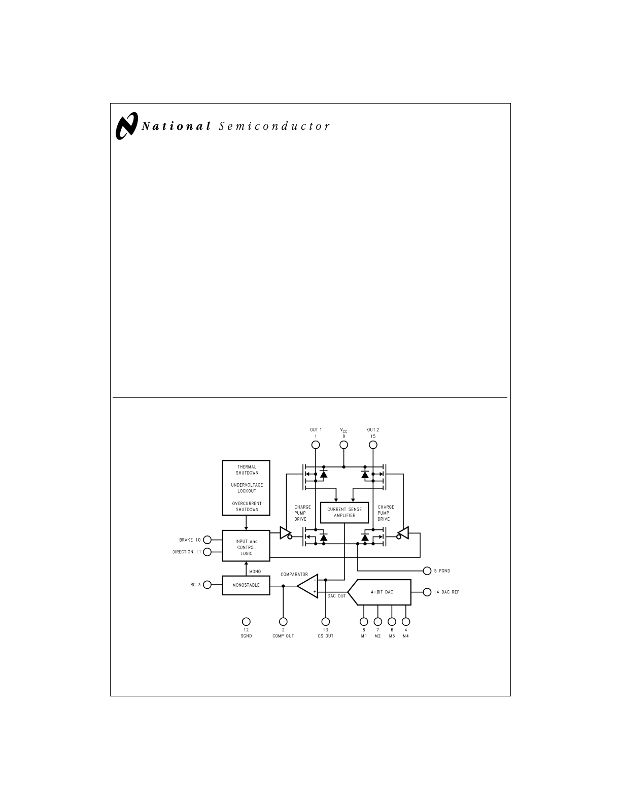
Functional Block and Connection Diagram
(15-Lead TO-220 Molded Power Package (T) )
DS011878-1
Order Number LMD18245T
See NS Package Number TA15A
April 1998
LMD18245
3A,
55V
DMOS
Full-Bridge
Motor
Driver
© 1998 National Semiconductor Corporation
DS011878
www.national.com

Absolute Maximum Ratings
(Note 1)
If Military/Aerospace specified devices are required,
please contact the National Semiconductor Sales Office/
Distributors for availability and specifications.
DC Voltage at:
OUT 1, V
CC
, and OUT 2
+60V
COMP OUT, RC, M4, M3, M2, M1, BRAKE,
+12V
DIRECTION, CS OUT, and DAC REF
DC Voltage PGND to SGND
±
400mV
Continuous Load Current
3A
Peak Load Current (Note 2)
6A
Junction Temperature (T
J(max)
)
+150˚C
Power Dissipation (Note 3) :
TO-220 (T
A
= 25˚C, Infinite Heatsink)
25W
TO-220 (T
A
= 25˚C, Free Air)
3.5W
ESD Susceptibility (Note 4)
1500V
Storage Temperature Range (T
S
)
−40˚C to +150˚C
Lead Temperature (Soldering, 10 seconds)
300˚C
Operating Conditions
(Note 1)
Temperature Range (T
J
) (Note 3)
−40˚C to +125˚C
Supply Voltage Range (V
CC
)
+12V to +55V
CS OUT Voltage Range
0V to +5V
DAC REF Voltage Range
0V to +5V
MONOSTABLE Pulse Range
10 µs to 100 ms
Electrical Characteristics
(Note 2)
The following specifications apply for V
CC
= +42V, unless otherwise stated. Boldface limits apply over the operating tem-
perature range, −40˚C
≤
T
J
≤
+125˚C. All other limits apply for T
A
= T
J
= 25˚C.
Symbol
Parameter
Conditions
Typical
Limit
Units
(Note 5)
(Note 5)
(Limits)
I
CC
Quiescent Supply Current
DAC REF = 0V, V
CC
= +20V
8
mA
15
mA (max)
POWER OUTPUT STAGE
R
DS(ON)
Switch ON Resistance
I
LOAD
= 3A
0.3
0.4
Ω
(max)
0.6
Ω
(max)
I
LOAD
= 6A
0.3
0.4
Ω
(max)
0.6
Ω
(max)
V
DIODE
Body Diode Forward Voltage
I
DIODE
= 3A
1.0
V
1.5
V(max)
T
rr
Diode Reverse Recovery Time
I
DIODE
= 1A
80
ns
Q
rr
Diode Reverse Recovery Charge
I
DIODE
= 1A
40
nC
t
D(ON)
Output Turn ON Delay Time
Sourcing Outputs
I
LOAD
= 3A
5
µs
Sinking Outputs
I
LOAD
= 3A
900
ns
t
D(OFF)
Output Turn OFF Delay Time
Sourcing Outputs
I
LOAD
= 3A
600
ns
Sinking Outputs
I
LOAD
= 3A
400
ns
t
ON
Output Turn ON Switching Time
Sourcing Outputs
I
LOAD
= 3A
40
µs
Sinking Outputs
I
LOAD
= 3A
1
µs
t
OFF
Output Turn OFF Switching Time
Sourcing Outputs
I
LOAD
= 3A
200
ns
Sinking Outputs
I
LOAD
= 3A
80
ns
t
pw
Minimum Input Pulse Width
Pins 10 and 11
2
µs
t
DB
Minimum Dead Band
(Note 6)
40
ns
CURRENT SENSE AMPLIFIER
Current Sense Output
I
LOAD
= 1A (Note 7)
200
µA (min)
250
175
µA (min)
300
µA (max)
325
µA (max)
Current Sense Linearity Error
0.5A
≤
I
LOAD
≤
3A (Note 7)
±
6
%
±
9
%(max)
Current Sense Offset
I
LOAD
= 0A
5
µA
20
µA (max)
www.national.com
2

Electrical Characteristics
(Note 2) (Continued)
The following specifications apply for V
CC
= +42V, unless otherwise stated. Boldface limits apply over the operating tem-
perature range, −40˚C
≤
T
J
≤
+125˚C. All other limits apply for T
A
= T
J
= 25˚C.
Symbol
Parameter
Conditions
Typical
Limit
Units
(Note 5)
(Note 5)
(Limits)
DIGITAL-TO-ANALOG CONVERTER (DAC)
Resolution
4
Bits (min)
Monotonicity
4
Bits (min)
Total Unadjusted Error
0.125
0.25
LSB (max)
0.5
LSB (max)
Propagation Delay
50
ns
I
REF
DAC REF Input Current
DAC REF = +5V
−0.5
µA
±
10
µA (max)
COMPARATOR AND MONOSTABLE
Comparator High Output Level
6.27
V
Comparator Low Output Level
88
mV
Comparator Output Current
Source
0.2
mA
Sink
3.2
mA
t
DELAY
Monostable Turn OFF Delay
(Note 8)
1.2
µs
2.0
µs (max)
PROTECTION AND PACKAGE THERMAL RESISTANCES
Undervoltage Lockout, V
CC
5
V (min)
8
V (max)
T
JSD
Shutdown Temperature, T
J
155
˚C
Package Thermal Resistances
θ
JC
Junction-to-Case, TO-220
1.5
˚C/W
θ
JA
Junction-to-Ambient, TO-220
35
˚C/W
LOGIC INPUTS
V
IL
Low Level Input Voltage
−0.1
V (min)
0.8
V (max)
V
IH
High Level Input Voltage
2
V (min)
12
V (max)
I
IN
Input Current
V
IN
= 0V or 12V
±
10
µA (max)
Note 1: Absolute Maximum Ratings indicate limits beyond which damage to the device may occur. Electrical specifications do not apply when operating the device
outside the rated Operating Conditions.
Note 2: Unless otherwise stated, load currents are pulses with widths less than 2 ms and duty cycles less than 5%.
Note 3: The maximum allowable power dissipation at any ambient temperature is P
Max
= (125 − T
A
)/
θ
JA
, where 125˚C is the maximum junction temperature for op-
eration, T
A
is the ambient temperature in ˚C, and
θ
JA
is the junction-to-ambient thermal resistance in ˚C/W. Exceeding P
max
voids the Electrical Specifications by forc-
ing T
J
above 125˚C. If the junction temperature exceeds 155˚C, internal circuitry disables the power bridge. When a heatsink is used,
θ
JA
is the sum of the
junction-to-case thermal resistance of the package,
θ
JC
, and the case-to-ambient thermal resistance of the heatsink.
Note 4: ESD rating is based on the human body model of 100 pF discharged through a 1.5 k
Ω
resistor. M1, M2, M3 and M4, pins 8, 7, 6 and 4 are protected to 800V.
Note 5: All limits are 100% production tested at 25˚C. Temperature extreme limits are guaranteed via correlation using accepted SQC (Statistical Quality Control)
methods. All limits are used to calculate AOQL (Average Outgoing Quality Level). Typicals are at T
J
= 25˚C and represent the most likely parametric norm.
Note 6: Asymmetric turn OFF and ON delay times and switching times ensure a switch turns OFF before the other switch in the same half H-bridge begins to turn
ON (preventing momentary short circuits between the power supply and ground). The transitional period during which both switches are OFF is commonly referred
to as the dead band.
Note 7: (I
LOAD
, I
SENSE
) data points are taken for load currents of 0.5A, 1A, 2A and 3A. The current sense gain is specified as I
SENSE
/I
LOAD
for the 1A data point.
The current sense linearity is specified as the slope of the line between the 0.5A and 1A data points minus the slope of the line between the 2A and 3A data points
all divided by the slope of the line between the 0.5A and 1A data points.
Note 8: Turn OFF delay, t
DELAY
, is defined as the time from the voltage at the output of the current sense amplifier reaching the DAC output voltage to the lower
DMOS switch beginning to turn OFF. With V
CC
= 32V, DIRECTION high, and 200
Ω
connected between OUT1 and V
CC
, the voltage at RC is increased from 0V to
5V at 1.2V/µs, and t
DELAY
is measured as the time from the voltage at RC reaching 2V to the time the voltage at OUT 1 reaches 3V.
3
www.national.com
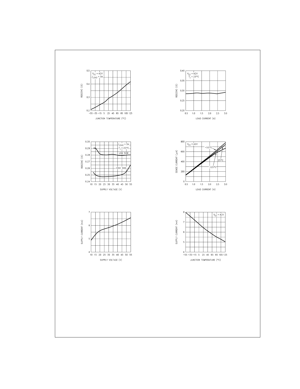
Typical Performance Characteristics
RDS(ON) vs Temperature
DS011878-29
RDS(ON) vs Load Current
DS011878-30
RDS(ON) vs
Supply Voltage
DS011878-31
Current Sense Output
vs Load Current
DS011878-32
Supply Current vs
Supply Voltage
DS011878-33
Supply Current vs
Temperature
DS011878-34
www.national.com
4
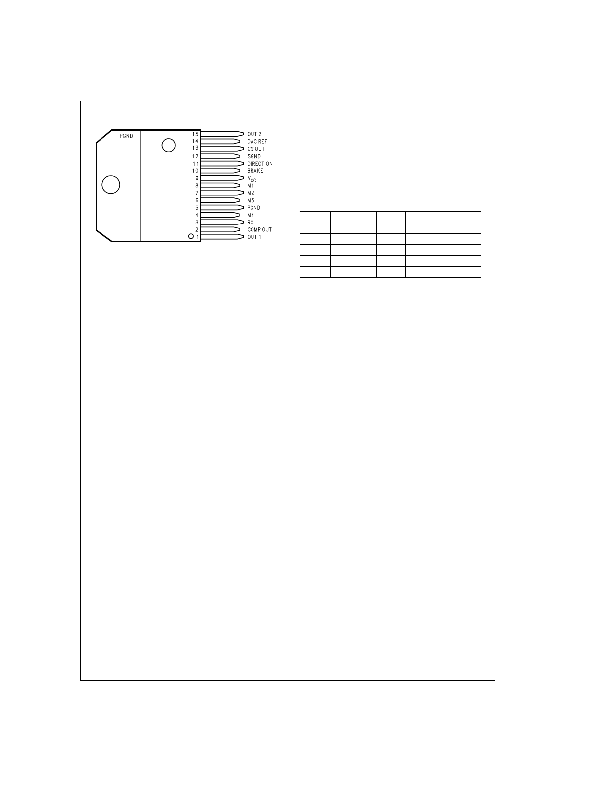
Connection Diagram
Pinout Descriptions
(See Functional Block
and Connection Diagrams)
Pin 1, OUT 1: Output node of the first half H-bridge.
Pin 2, COMP OUT: Output of the comparator. If the voltage
at CS OUT exceeds that provided by the DAC, the compara-
tor triggers the monostable.
Pin 3, RC: Monostable timing node. A parallel resistorca-
pacitor network connected between this node and ground
sets the monostable timing pulse at about 1.1 RC seconds.
Pin 5, PGND: Ground return node of the power bridge. Bond
wires (internaI) connect PGND to the tab of the TO-220
package.
Pins 4 and 6 through 8, M4 through M1: Digital inputs of
the DAC. These inputs make up a four-bit binary number
with M4 as the most significant bit or MSB. The DAC pro-
vides an analog voltage directly proportional to the binary
number applied at M4 through M1.
Pin 9, V
CC
: Power supply node.
Pin 10, BRAKE: Brake logic input. Pulling the BRAKE input
logic-high activates both sourcing switches of the power
bridge — effectively shorting the load. See
Table 1
. Shorting
the load in this manner forces the load current to recirculate
and decay to zero.
Pin 11, DIRECTION: Direction logic input. The logic level at
this input dictates the direction of current flow in the load.
See
Table 1
.
Pin 12, SGND: Ground return node of all signal level circuits.
Pin 13, CS OUT: Output of the current sense amplifier. The
current sense amplifier sources 250 µA (typical) per ampere
of total forward current conducted by the upper two switches
of the power bridge.
Pin 14, DAC REF: Voltage reference input of the DAC. The
DAC provides an analog voltage equal to V
DAC REF
x D/16,
where D is the decimal equivalent (0–15) of the binary num-
ber applied at M4 through M1.
Pin 15, OUT 2: Output node of the second half H-bridge.
TABLE 1. Switch Control Logic Truth Table
BRAKE
DIRECTION
MONO
Active Switches
H
X
X
Source 1, Source 2
L
H
L
Source 2
L
H
H
Source 2, Sink 1
L
L
L
Source 1
L
L
H
Source 1, Sink 2
X = don’t care
MONO is the output of the monostable.
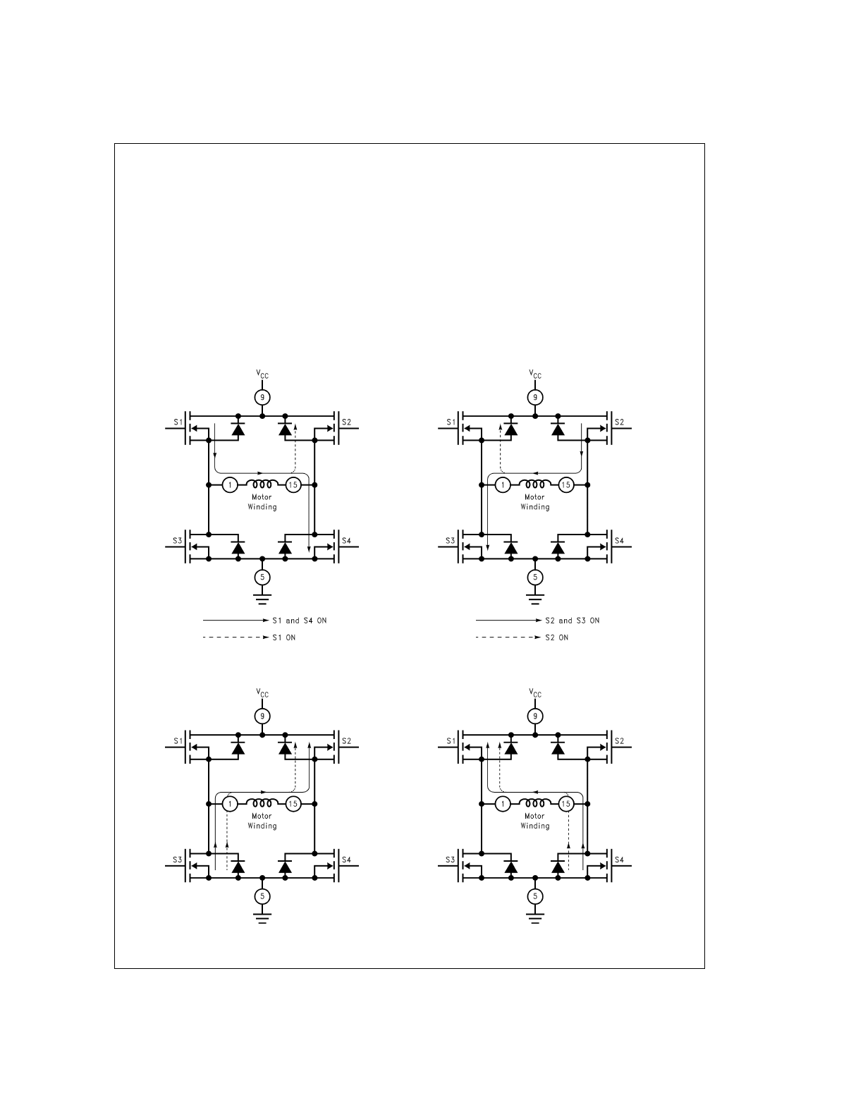
Functional Descriptions
TYPICAL OPERATION OF A CHOPPER AMPLIFIER
Chopper amplifiers employ feedback driven switching of a
power bridge to control and limit current in the winding of a
motor (
Figure 1
). The bridge consists of four solid state
power switches and four diodes connected in an H configu-
ration. Control circuitry (not shown) monitors the winding
current and compares it to a threshold. While the winding
current remains less than the threshold, a source switch and
a sink switch in opposite halves of the bridge force the sup-
ply voltage across the winding, and the winding current in-
creases rapidly towards V
CC
/R (
Figure 1a
and
Figure 1d
).
As the winding current surpasses the threshold, the control
circuitry turns OFF the sink switch for a fixed period or
off-time.
During the off-time, the source switch and the oppo-
site upper diode short the winding, and the winding current
recirculates and decays slowly towards zero (
Figure 1b
and
Figure 1e
). At the end of the off-time, the control circuitry
turns back ON the sink switch, and the winding current again
increases rapidly towards V
CC
/R (
Figure 1a
and
Figure 1d
again). The above sequence repeats to provide a current
chopping action that limits the winding current to the thresh-
old (
Figure 1g
). Chopping only occurs if the winding current
reaches the threshold. During a change in the direction of
the winding current, the diodes provide a decay path for the
initial winding current (
Figure 1c
and
Figure 1f
). Since the
bridge shorts the winding for a fixed period, this type of chop-
per amplifier is commonly referred to as a
fixed off-time
chopper.
DS011878-2
Top View
15-Lead TO-220 Molded Power Package
Order Number LMD18245T
See NS Package Number TA15A
5
www.national.com
Functional Descriptions
(Continued)
(a)
DS011878-3
(b)
DS011878-4
(c)
DS011878-5
(d)
DS011878-6
(e)
DS011878-7
(f)
DS011878-8
(g)
DS011878-9
FIGURE 1. Chopper Amplifier Chopping States: Full V
CC
Applied Across the Winding (a) and (d), Shorted Winding (b)
and (e), Winding Current Decays During a Change in the Direction of the Winding Current (c) and (f), and the
Chopped Winding Current (g)
www.national.com
6
Functional Descriptions
(Continued)
THE LMD18245 CHOPPER AMPLIFIER
The LMD18245 incorporates all the circuit blocks needed to
implement a fixed off-time chopper amplifier. These blocks
include: an all DMOS, full H-bridge with clamp diodes, an
amplifier for sensing the load current, a comparator, a
monostable, and a DAC for digital control of the chopping
threshold. Also incorporated are logic, level shifting and drive
blocks for digital control of the direction of the load current
and braking.
THE H-BRIDGE
The power stage consists of four DMOS power switches and
associated body diodes connected in an H-bridge configura-
tion (
Figure 2
). Turning ON a source switch and a sink
switch in opposite halves of the bridge forces the full supply
voltage less the switch drops across the motor winding.
While the bridge remains in this state, the winding current in-
creases exponentially towards a limit dictated by the supply
voltage, the switch drops, and the winding resistance. Sub-
sequently turning OFF the sink switch causes a voltage tran-
sient that forward biases the body diode of the other source
switch. The diode clamps the transient at one diode drop
above the supply voltage and provides an alternative current
path. While the bridge remains in this state, it essentially
shorts the winding and the winding current recirculates and
decays exponentially towards zero. During a change in the
direction of the winding current, both the switches and the
body diodes provide a decay path for the initial winding cur-
rent (
Figure 3
).
DS011878-10
DS011878-11
FIGURE 2. The DMOS H-Bridge
DS011878-12
DS011878-13
FIGURE 3. Decay Paths for Initial Winding Current During a Change in the Direction of the Winding Current
7
www.national.com
Functional Descriptions
(Continued)
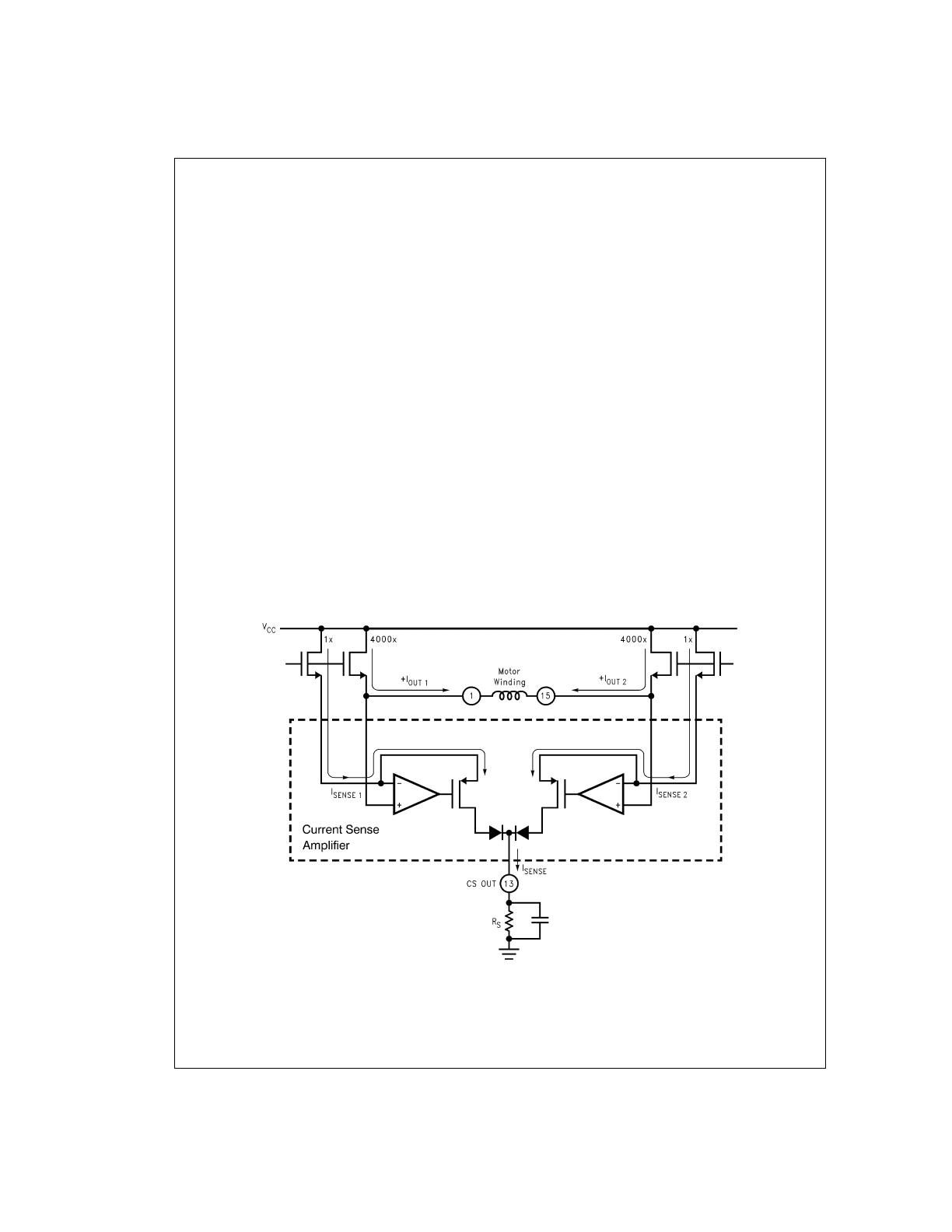
THE CURRENT SENSE AMPLIFIER
Many transistor cells in parallel make up the DMOS power
switches. The current sense amplifier (
Figure 4
) uses a
small fraction of the cells of both upper switches to provide a
unique, low-loss means for sensing the load current. In prac-
tice, each upper switch functions as a 1x sense device in
parallel with a 4000x power device. The current sense ampli-
fier forces the voltage at the source of the sense device to
equal that at the source of the power device; thus, the de-
vices share the total drain current in proportion to the 1:4000
cell ratio. Only the current flowing from drain to source, the
forward current, registers at the output of the current sense
amplifier. The current sense amplifier, therefore, sources
250 µA per ampere of total forward current conducted by the
upper two switches of the power bridge.
The sense current develops a potential across R
S
that is pro-
portional to the load current; for example, per ampere of load
current, the sense current develops one volt across a 4 k
Ω
resistor (the product of 250 µA per ampere and 4 k
Ω
). Since
chopping of the load current occurs as the voltage at CS
OUT surpasses the threshold (the DAC output voltage), R
S
sets the gain of the chopper amplifier; for example, a 2 k
Ω
resistor sets the gain at two amperes of load current per volt
of the threshold (the reciprocal of the product of 250 µA per
ampere and 2 k
Ω
). A quarter watt resistor suffices. A low
value capacitor connected in parallel with R
S
filters the ef-
fects of switching noise from the current sense signal.
While the specified maximum DC voltage compliance at CS
OUT is 12V, the specified operating voltage range at CS
OUT is 0V to 5V.
THE DIGITAL-TO-ANALOG CONVERTER (DAC)
The DAC sets the threshold voltage for chopping at
V
DAC REF
x D/16, where D is the decimal equivalent (0–15)
of the binary number applied at M4 through M1, the digital in-
puts of the DAC. M4 is the MSB or most significant bit. For
applications that require higher resolution, an external DAC
can drive the DAC REF input. While the specified maximum
DC voltage compliance at DAC REF is 12V, the specified op-
erating voltage range at DAC REF is 0V to 5V.
THE COMPARATOR, MONOSTABLE AND WINDING
CURRENT THRESHOLD FOR CHOPPING
As the voltage at CS OUT surpasses that at the output of the
DAC, the comparator triggers the monostable, and the
monostable, once triggered, provides a timing pulse to the
control logic. During the timing pulse, the power bridge
shorts the motor winding, causing current in the winding to
recirculate and decay slowly towards zero (
Figure 1b
and
Figure 1e
again). A parallel resistor-capacitor network con-
nected between RC (pin
#
3) and ground sets the timing
pulse or off-time at about 1.1 RC seconds.
Chopping of the winding current occurs as the voltage at CS
OUT exceeds that at the output of the DAC; so chopping oc-
curs at a winding current threshold of about
(V
DAC REF
x D/16)
÷
((250 x 10
−6
) x R
S
)) amperes.
DS011878-14
FIGURE 4. The Source Switches of the Power Bridge and the Current Sense Amplifier
www.national.com
8
Applications Information
POWER SUPPLY BYPASSING
Step changes in current drawn from the power supply occur
repeatedly during normal operation and may cause large
voltage spikes across inductance in the power supply line.
Care must be taken to limit voltage spikes at V
CC
to less than
the 60V Absolute Maximum Rating. At a change in the direc-
tion of the load current, the initial load current tends to raise
the voltage at the power supply rail (
Figure 3
) again. Current
transients caused by the reverse recovery of the clamp di-
odes tend to pull down the voltage at the power supply rail.
Bypassing the power supply line at V
CC
is required to protect
the device and minimize the adverse effects of normal op-
eration on the power supply rail. Using both a 1 µF high fre-
quency ceramic capacitor and a large-value aluminum elec-
trolytic capacitor is highly recommended. A value of 100 µF
per ampere of load current usually suffices for the aluminum
electrolytic capacitor. Both capacitors should have short
leads and be located within one half inch of V
CC
.
OVERCURRENT PROTECTION
If the forward current in either source switch exceeds a 12A
threshold, internal circuitry disables both source switches,
forcing a rapid decay of the fault current (
Figure 5
). Approxi-
mately 3 µs after the fault current reaches zero, the device
restarts. Automatic restart allows an immediate return to nor-
mal operation once the fault condition has been removed. If
the fault persists, the device will begin cycling into and out of
thermal shutdown. Switching large fault currents may cause
potentially destructive voltage spikes across inductance in
the power supply line; therefore, the power supply line must
be properly bypassed at V
CC
for the motor driver to survive
an extended overcurrent fault.
In the case of a locked rotor, the inductance of the winding
tends to limit the rate of change of the fault current to a value
easily handled by the protection circuitry. In the case of a low
inductance short from either output to ground or between
outputs, the fault current could surge past the 12A shutdown
threshold, forcing the device to dissipate a substantial
amount of power for the brief period required to disable the
source switches. Because the fault power must be dissi-
pated by only one source switch, a short from output to
ground represents the worst case fault. Any overcurrent fault
is potentially destructive, especially while operating with high
supply voltages (
≥
30V), so precautions are in order. Sinking
V
CC
for heat with 1 square inch of 1 ounce copper on the
printed circuit board is highly recommended. The sink
switches are not internally protected against shorts to V
CC
.
THERMAL SHUTDOWN
Internal circuitry senses the junction temperature near the
power bridge and disables the bridge if the junction tempera-
ture exceeds about 155˚C. When the junction temperature
cools past the shutdown threshold (lowered by a slight hys-
teresis), the device automatically restarts.
UNDERVOLTAGE LOCKOUT
Internal circuitry disables the power bridge if the power sup-
ply voltage drops below a rough threshold between 8V and
5V. Should the power supply voltage then exceed the thresh-
old, the device automatically restarts.
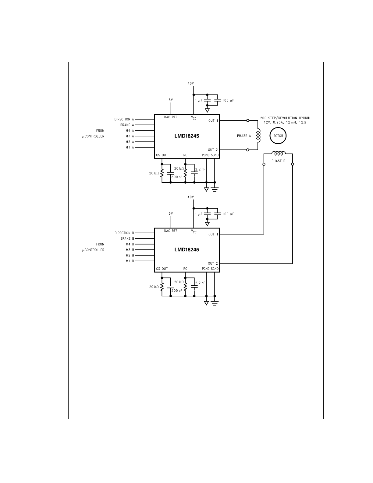
The Typical Application
Figure 6
shows the typical application, the power stage of a
chopper drive for bipolar stepper motors. The 20 k
Ω
resistor
and 2.2 nF capacitor connected between RC and ground set
the off-time at about 48 µs, and the 20 k
Ω
resistor connected
between CS OUT and ground sets the gain at about 200 mA
per volt of the threshold for chopping. Digital signals control
the thresholds for chopping, the directions of the winding
currents, and, by extension, the drive type (full step, half
step, etc.). A µprocessor or µcontroller usually provides the
digital control signals.
DS011878-15
Trace: Fault Current at 5A/div
Horizontal: 20 µs/div
FIGURE 5. Fault Current with V
CC
= 30V, OUT 1 Shorted to OUT 2, and CS OUT Grounded
9
www.national.com
The Typical Application
(Continued)
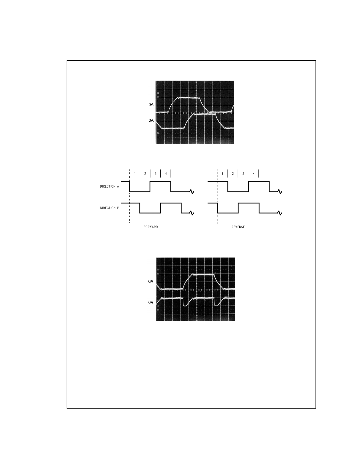
ONE-PHASE-ON FULL STEP DRIVE (WAVE DRIVE)
To make the motor take full steps, windings A and B can be
energized in the sequence
A
→
B
→
A
*
→
B
*
→
A
→
…,
where A represents winding A energized with current in one
direction and A
*
represents winding A energized with current
in the opposite direction. The motor takes one full step each
time one winding is de-energized and the other is energized.
To make the motor step in the opposite direction, the order of
the above sequence must be reversed.
Figure 7
shows the
winding currents and digital control signals for a wave drive
application of the typical application circuit.
TWO-PHASE-ON FULL STEP DRIVE
To make the motor take full steps, windings A and B can also
be energized in the sequence
AB
→
A
*
B
→
A
*
B
*
→
AB
*
→
AB
→
…,
and because both windings are energized at all times, this
sequence produces more torque than that produced with
wave drive. The motor takes one full step at each change of
direction of either winding current.
Figure 8
shows the wind-
ing currents and digital control signals for this application of
the typical application circuit, and
Figure 9
shows, for a
single phase, the winding current and voltage at the output of
the associated current sense amplifier.
DS011878-16
FIGURE 6. Typical Application Circuit for Driving Bipolar Stepper Motors
www.national.com
10

The Typical Application
(Continued)
DS011878-17
Top Trace: Phase A Winding Current at 1A/div
Bottom Trace: Phase B Winding Current at 1A/div
Horizontal: 1 ms/div
*500 steps/second
DS011878-18
BRAKE A = BRAKE B = 0
FIGURE 7. Winding Currents and Digital Control Signals for One-Phase-On Drive (Wave Drive)
11
www.national.com
The Typical Application
(Continued)
HALF STEP DRIVE WITHOUT TORQUE
COMPENSATION
To make the motor take half steps, windings A and B can be
energized in the sequence
A
→
AB
→
B
→
A
*
B
→
A
*
→
A
*
B
*
→
B
*
→
AB
*
→
A
→
…
The motor takes one half step each time the number of en-
ergized windings changes. It is important to note that al-
though half stepping doubles the step resolution, changing
the number of energized windings from two to one de-
creases (one to two increases) torque by about 40%, result-
ing in significant torque ripple and possibly noisy operation.
Figure 10
shows the winding currents and digital control sig-
nals for this half step application of the typical application
circuit.
DS011878-19
Top Trace: Phase A Winding Current at 1A/div
Bottom Trace: Phase B Winding Current at 1A/div
Horizontal: 1 ms/div
*500 steps/second
DS011878-20
M4 A through M1 A = M4 B through M1 B = 1
BRAKE A = BRAKE B = 0
FIGURE 8. Winding Currents and Digital Control Signals for Two-Phase-On Drive
DS011878-21
Top Trace: Phase A Winding Current at 1A/div
Bottom Trace: Phase A Sense Voltage at 5V/div
Horizontal: 1 ms/div
*500 steps/second
FIGURE 9. Winding Current and Voltage at the Output of the Associated Current Sense Amplifier
www.national.com
12
The Typical Application
(Continued)
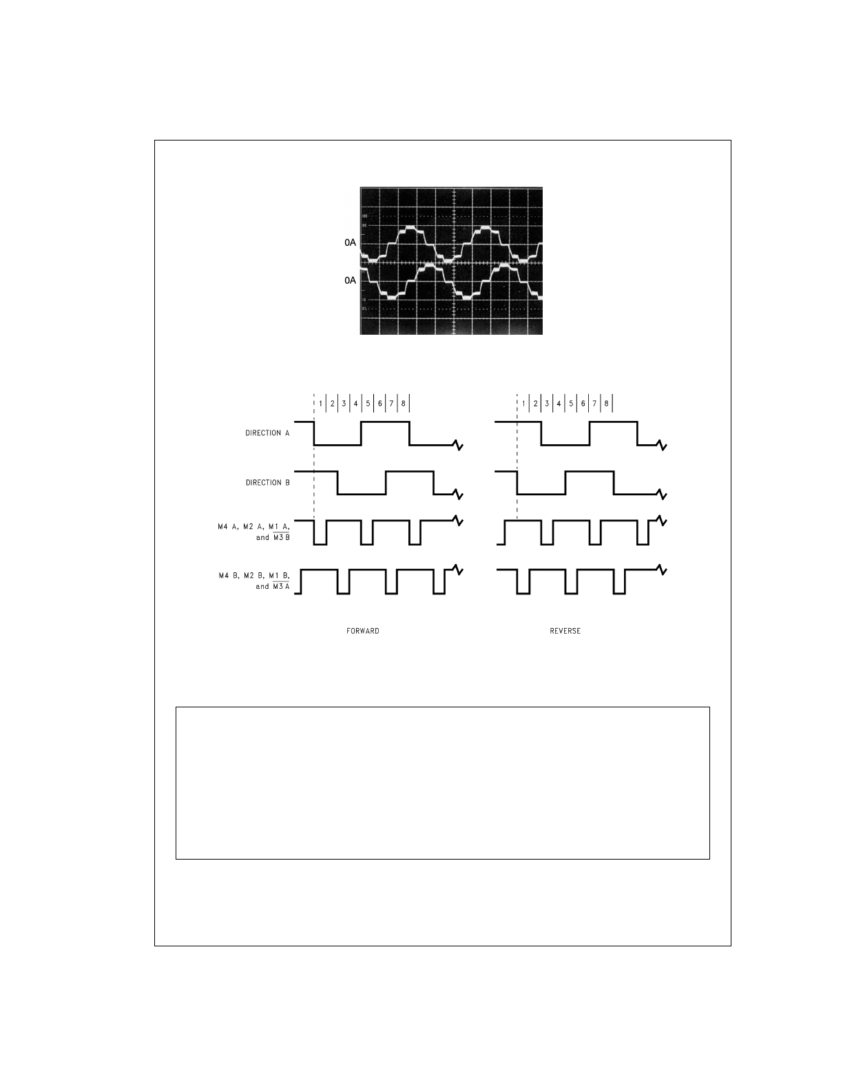
HALF STEP DRIVE WITH TORQUE COMPENSATION
To make the motor take half steps, the windings can also be
energized with sinusoidal currents (
Figure 11
). Controlling
the winding currents in the fashion shown doubles the step
resolution without the significant torque ripple of the prior
drive technique. The motor takes one half step each time the
level of either winding current changes. Half step drive with
torque compensation is microstepping drive. Along with the
obvious advantage of increased step resolution, microstep-
ping reduces both full step oscillations and resonances that
occur as the motor and load combination is driven at its natu-
ral resonant frequency or subharmonics thereof. Both of
these advantages are obtained by replacing full steps with
bursts of microsteps. When compared to full step drive, the
motor runs smoother and quieter.
Figure 12
shows the lookup table for this application of the
typical application circuit. Dividing 90˚electrical per full step
by two microsteps per full step yields 45˚ electrical per mi-
crostep.
α
, therefore, increases from 0 to 315˚ in increments
of 45˚. Each full 360˚ cycle comprises eight half steps.
Rounding |cos
α
| to four bits gives D A, the decimal equiva-
lent of the binary number applied at M4 A through M1 A. DI-
RECTION A controls the polarity of the current in winding A.
Figure 11
shows the sinusoidal winding currents.
DS011878-22
Top Trace: Phase A Winding Current at 1A/div
Bottom Trace: Phase B Winding Current at 1A/div
Horizontal: 1 ms/div
*500 steps/second
DS011878-23
BRAKE A = BRAKE B = 0
FIGURE 10. Winding Currents and Digital Control Signals for Half Step Drive without Torque Compensation
13
www.national.com
The Typical Application
(Continued)
DS011878-24
Top Trace: Phase A Winding Current at 1A/div
Bottom Trace: Phase B Winding Current at 1A/div
Horizontal: 2 ms/div
*500 steps/second
DS011878-25
BRAKE A = BRAKE B = 0
90˚ ELECTRICAL/FULL STEP
÷
2 MICROSTEPS/FULL STEP = 45˚ ELECTRICAL/MICROSTEP
FIGURE 11. Winding Currents and Digital Control Signals for Half Step Drive with Torque Compensation
|
FORWARD
↓
α
|cos(
α
)|
D A
DIRECTION A
|sin(
α
)|
D B
DIRECTlON B
0
1
15
1
0
0
1
45
0.707
11
1
0.707
11
1
90
0
0
0
1
15
1
135
0.707
11
0
0.707
11
1
↑
180
1
15
0
0
0
0
REVERSE
225
0.707
11
0
0.707
11
0
|
270
0
0
1
1
15
0
315
0.707
11
1
0.707
11
0
REPEAT
FIGURE 12. Lookup Table for Half Step Drive with Torque Compensation
www.national.com
14
The Typical Application
(Continued)
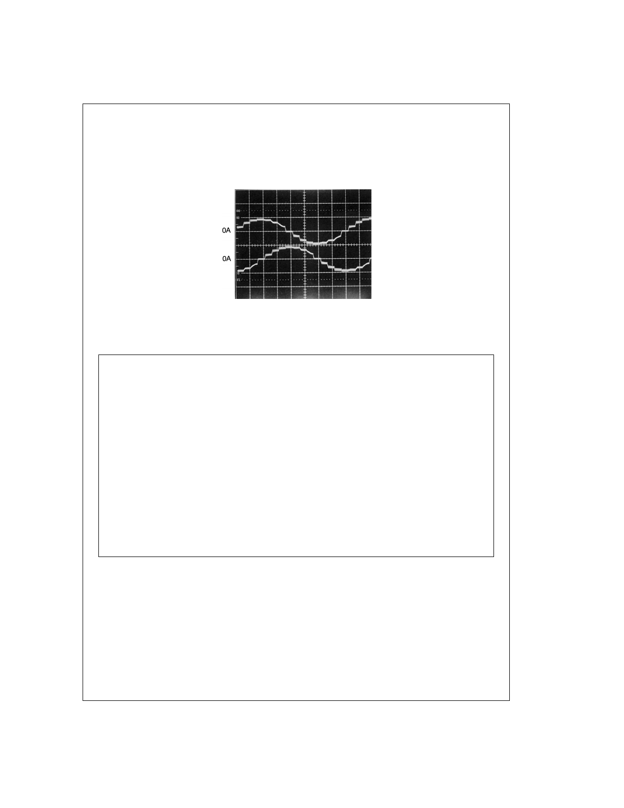
QUARTER STEP DRIVE WITH TORQUE
COMPENSATION
Figure 13
shows the winding currents and lookup table for a
quarter step drive (four microsteps per full step) with torque
compensation.
DS011878-26
Top Trace: Phase A Winding Current at 1A/div
Bottom Trace: Phase B Winding Current at 1A/div
Horizontal: 2ms/div
*250 steps/second
90˚ ELECTRICAL/FULL STEP
÷
4 MICROSTEPS/FULL STEP = 22.5˚ ELECTRICAL/MICROSTEP
α
|cos(
α
)|
D A
DIRECTION A
|sin(
α
)|
D B
DIRECTION B
0
1
15
1
0
0
1
22.5
0.924
14
1
0.383
6
1
|
45
0.707
11
1
0.707
11
1
FORWARD
67.5
0.383
6
1
0.924
14
1
↓
90
0
0
0
1
15
1
112.5
0.383
6
0
0.924
14
1
↑
135
0.707
11
0
0.707
11
1
REVERSE
157.5
0.924
14
0
0.383
6
1
|
180
1
15
0
0
0
0
202.5
0.924
14
0
0.383
6
0
225
0.707
11
0
0.707
11
0
247.5
0.383
6
0
0.924
14
0
270
0
0
1
1
15
0
292.5
0.383
6
1
0.924
14
0
315
0.707
11
1
0.707
11
0
337.5
0.924
14
1
0.383
6
0
REPEAT
BRAKE A = BRAKE B = 0
FIGURE 13. Winding Currents and Lookup Table for Quarter Step Drive with Torque Compensation
15
www.national.com
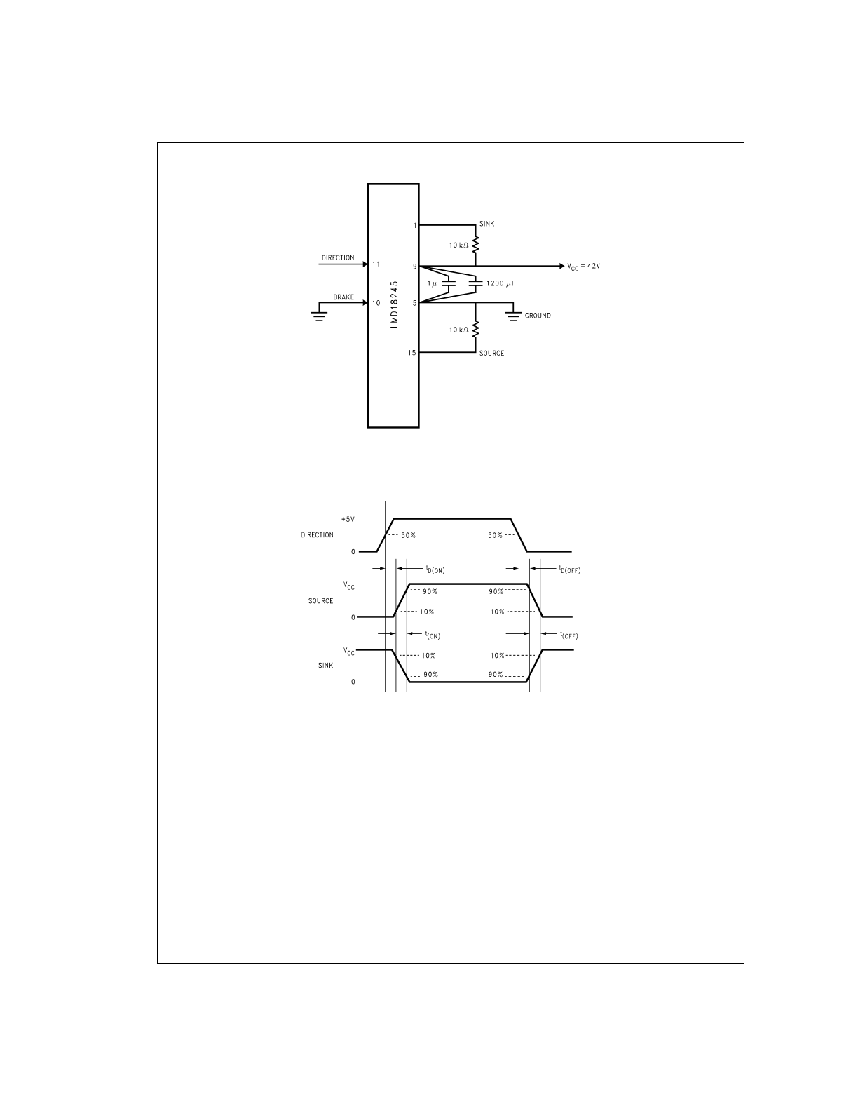
Test Circuit and Switching Time Definitions
DS011878-28
www.national.com
16

17
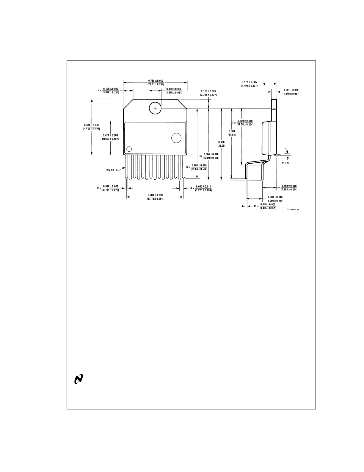
Physical Dimensions
inches (millimeters) unless otherwise noted
LIFE SUPPORT POLICY
NATIONAL’S PRODUCTS ARE NOT AUTHORIZED FOR USE AS CRITICAL COMPONENTS IN LIFE SUPPORT DE-
VICES OR SYSTEMS WITHOUT THE EXPRESS WRITTEN APPROVAL OF THE PRESIDENT OF NATIONAL SEMI-
CONDUCTOR CORPORATION. As used herein:
1. Life support devices or systems are devices or sys-
tems which, (a) are intended for surgical implant into
the body, or (b) support or sustain life, and whose fail-
ure to perform when properly used in accordance
with instructions for use provided in the labeling, can
be reasonably expected to result in a significant injury
to the user.
2. A critical component in any component of a life support
device or system whose failure to perform can be rea-
sonably expected to cause the failure of the life support
device or system, or to affect its safety or effectiveness.
National Semiconductor
Corporation
Americas
Tel: 1-800-272-9959
Fax: 1-800-737-7018
Email: support@nsc.com
www.national.com
National Semiconductor
Europe
Fax: +49 (0) 1 80-530 85 86
Email: europe.support@nsc.com
Deutsch Tel: +49 (0) 1 80-530 85 85
English
Tel: +49 (0) 1 80-532 78 32
Français Tel: +49 (0) 1 80-532 93 58
Italiano
Tel: +49 (0) 1 80-534 16 80
National Semiconductor
Asia Pacific Customer
Response Group
Tel: 65-2544466
Fax: 65-2504466
Email: sea.support@nsc.com
National Semiconductor
Japan Ltd.
Tel: 81-3-5620-6175
Fax: 81-3-5620-6179
15-Lead TO-220 Power Package (T)
Order Number LMD18245T
NS Package Number TA15A
LMD18245
3A,
55V
DMOS
Full-Bridge
Motor
Driver
National does not assume any responsibility for use of any circuitry described, no circuit patent licenses are implied and National reserves the right at any time without notice to change said circuitry and specifications.