
LMD18200
3A, 55V H-Bridge
General Description
The LMD18200 is a 3A H-Bridge designed for motion control
applications. The device is built using a multi-technology pro-
cess which combines bipolar and CMOS control circuitry
with DMOS power devices on the same monolithic structure.
Ideal for driving DC and stepper motors; the LMD18200 ac-
commodates peak output currents up to 6A. An innovative
circuit which facilitates low-loss sensing of the output current
has been implemented.
Features
n
Delivers up to 3A continuous output
n
Operates at supply voltages up to 55V
n
Low R
DS
(ON) typically 0.3
Ω
per switch
n
TTL and CMOS compatible inputs
n
No “shoot-through” current
n
Thermal warning flag output at 145˚C
n
Thermal shutdown (outputs off) at 170˚C
n
Internal clamp diodes
n
Shorted load protection
n
Internal charge pump with external bootstrap capability
Applications
n
DC and stepper motor drives
n
Position and velocity servomechanisms
n
Factory automation robots
n
Numerically controlled machinery
n
Computer printers and plotters
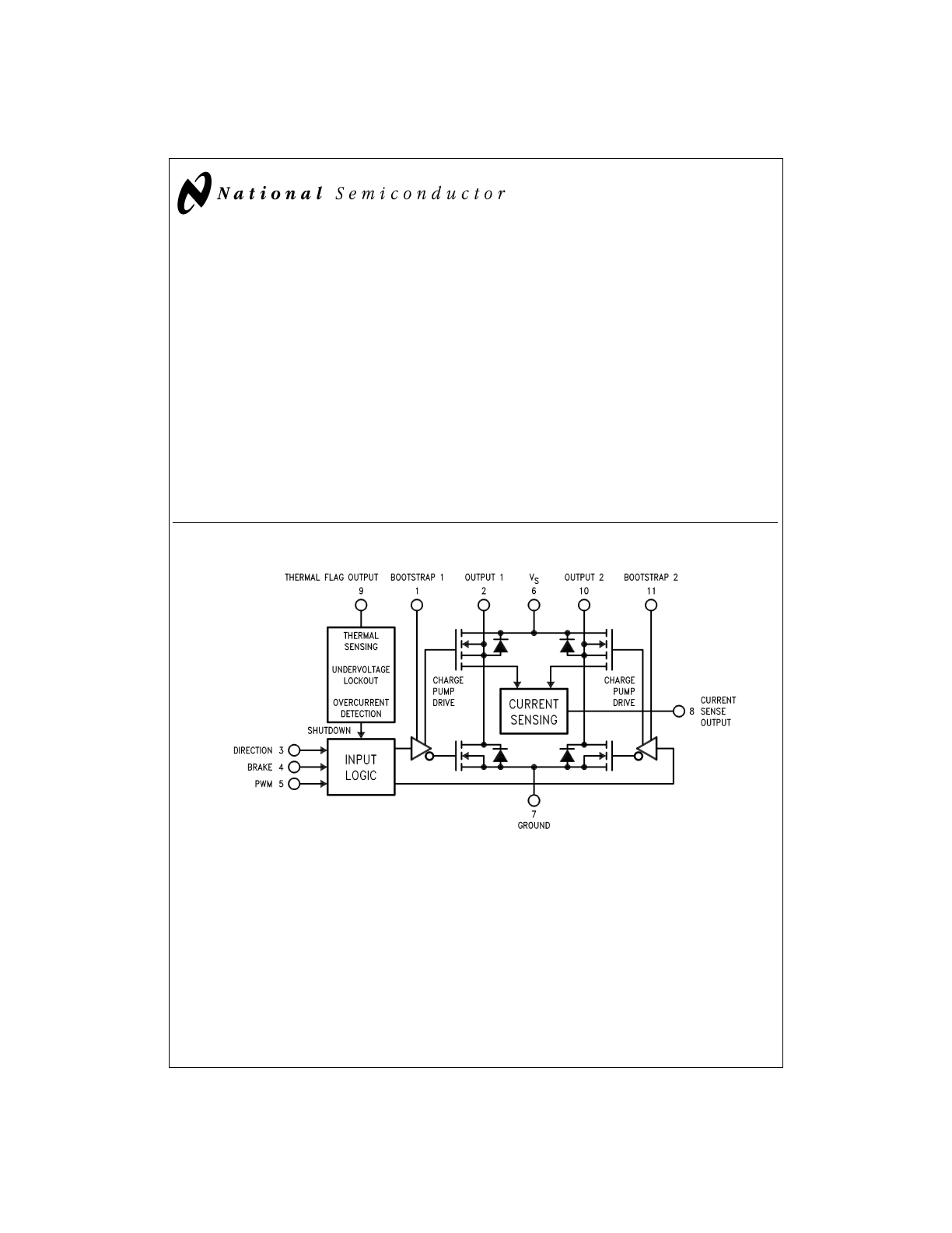
Functional Diagram
DS010568-1
FIGURE 1. Functional Block Diagram of LMD18200
April 1998
LMD18200
3A,
55V
H-Bridge
© 1998 National Semiconductor Corporation
DS010568
www.national.com
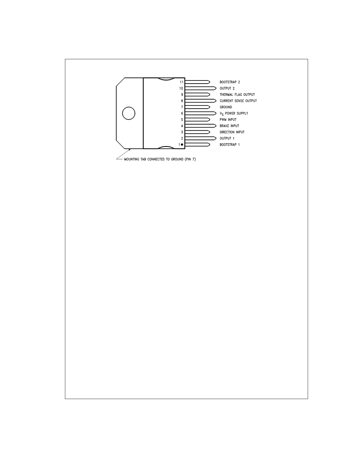
Connection Diagram and Ordering Information
DS010568-2
Top View
Order Number LMD18200T
See NS Package TA11B
www.national.com
2

Absolute Maximum Ratings
(Note 1)
If Military/Aerospace specified devices are required,
please contact the National Semiconductor Sales Office/
Distributors for availability and specifications.
Total Supply Voltage (V
S
, Pin 6)
60V
Voltage at Pins 3, 4, 5, 8 and 9
12V
Voltage at Bootstrap Pins
(Pins 1 and 11)
V
OUT
+16V
Peak Output Current (200 ms)
6A
Continuous Output Current (Note 2)
3A
Power Dissipation (Note 3)
25W
Power Dissipation (T
A
= 25˚C, Free Air)
3W
Junction Temperature, T
J(max)
150˚C
ESD Susceptibility (Note 4)
1500V
Storage Temperature, T
STG
−40˚C to +150˚C
Lead Temperature (Soldering, 10 sec.)
300˚C
Operating Ratings
(Note 1)
Junction Temperature, T
J
−40˚C to +125˚C
V
S
Supply Voltage
+12V to +55V
Electrical Characteristics
(Note 5)
The following specifications apply for V
S
= 42V, unless otherwise specified. Boldface limits apply over the entire operating
temperature range, −40˚C
≤
T
J
≤
+125˚C, all other limits are for T
A
= T
J
= 25˚C.
Symbol
Parameter
Conditions
Typ
Limit
Units
R
DS
(ON)
Switch ON Resistance
Output Current = 3A (Note 6)
0.33
0.4/0.6
Ω
(max)
R
DS
(ON)
Switch ON Resistance
Output Current = 6A (Note 6)
0.33
0.4/0.6
Ω
(max)
V
CLAMP
Clamp Diode Forward Drop
Clamp Current = 3A (Note 6)
1.2
1.5
V (max)
V
IL
Logic Low Input Voltage
Pins 3, 4, 5
−0.1
V (min)
0.8
V (max)
I
IL
Logic Low Input Current
V
IN
= −0.1V, Pins = 3, 4, 5
−10
µA (max)
V
IH
Logic High Input Voltage
Pins 3, 4, 5
2
V (min)
12
V (max)
I
IH
Logic High Input Current
V
IN
= 12V, Pins = 3, 4, 5
10
µA (max)
Current Sense Output
I
OUT
= 1A (Note 8)
377
325/300
µA (min)
425/450
µA (max)
Current Sense Linearity
1A
≤
I
OUT
≤
3A (Note 7)
±
6
±
9
%
Undervoltage Lockout
Outputs turn OFF
9
V (min)
11
V (max)
T
JW
Warning Flag Temperature
Pin 9
≤
0.8V, I
L
= 2 mA
145
˚C
V
F
(ON)
Flag Output Saturation Voltage
T
J
= T
JW
, I
L
= 2 mA
0.15
V
I
F
(OFF)
Flag Output Leakage
V
F
= 12V
0.2
10
µA (max)
T
JSD
Shutdown Temperature
Outputs Turn OFF
170
˚C
I
S
Quiescent Supply Current
All Logic Inputs Low
13
25
mA (max)
t
Don
Output Turn-On Delay Time
Sourcing Outputs, I
OUT
= 3A
300
ns
Sinking Outputs, I
OUT
= 3A
300
ns
t
on
Output Turn-On Switching Time
Bootstrap Capacitor = 10 nF
Sourcing Outputs, I
OUT
= 3A
100
ns
Sinking Outputs, I
OUT
= 3A
80
ns
t
Doff
Output Turn-Off Delay Times
Sourcing Outputs, I
OUT
= 3A
200
ns
Sinking Outputs, I
OUT
= 3A
200
ns
t
off
Output Turn-Off Switching Times
Bootstrap Capacitor = 10 nF
Sourcing Outputs, I
OUT
= 3A
75
ns
Sinking Outputs, I
OUT
= 3A
70
ns
t
pw
Minimum Input Pulse Width
Pins 3, 4 and 5
1
µs
t
cpr
Charge Pump Rise Time
No Bootstrap Capacitor
20
µs
3
www.national.com
Electrical Characteristics Notes
Note 1: Absolute Maximum Ratings indicate limits beyond which damage to the device may occur. DC and AC electrical specifications do not apply when op-
erating the device beyond its rated operating conditions.
Note 2: See Application Information for details regarding current limiting.
Note 3: The maximum power dissipation must be derated at elevated temperatures and is a function of T
J(max)
,
θ
JA
, and T
A
. The maximum allowable power dis-
sipation at any temperature is P
D(max)
= (T
J(max)
− T
A
)/
θ
JA
, or the number given in the Absolute Ratings, whichever is lower. The typical thermal resistance from junc-
tion to case (
θ
JC
) is 1.0˚C/W and from junction to ambient (
θ
JA
) is 30˚C/W. For guaranteed operation T
J(max)
= 125˚C.
Note 4: Human-body model, 100 pF discharged through a 1.5 k
Ω
resistor. Except Bootstrap pins (pins 1 and 11) which are protected to 1000V of ESD.
Note 5: All limits are 100% production tested at 25˚C. Temperature extreme limits are guaranteed via correlation using accepted SQC (Statistical Quality Control)
methods. All limits are used to calculate AOQL, (Average Outgoing Quality Level).
Note 6: Output currents are pulsed (t
W
<
2 ms, Duty Cycle
<
5%).
Note 7: Regulation is calculated relative to the current sense output value with a 1A load.
Note 8: Selections for tighter tolerance are available. Contact factory.
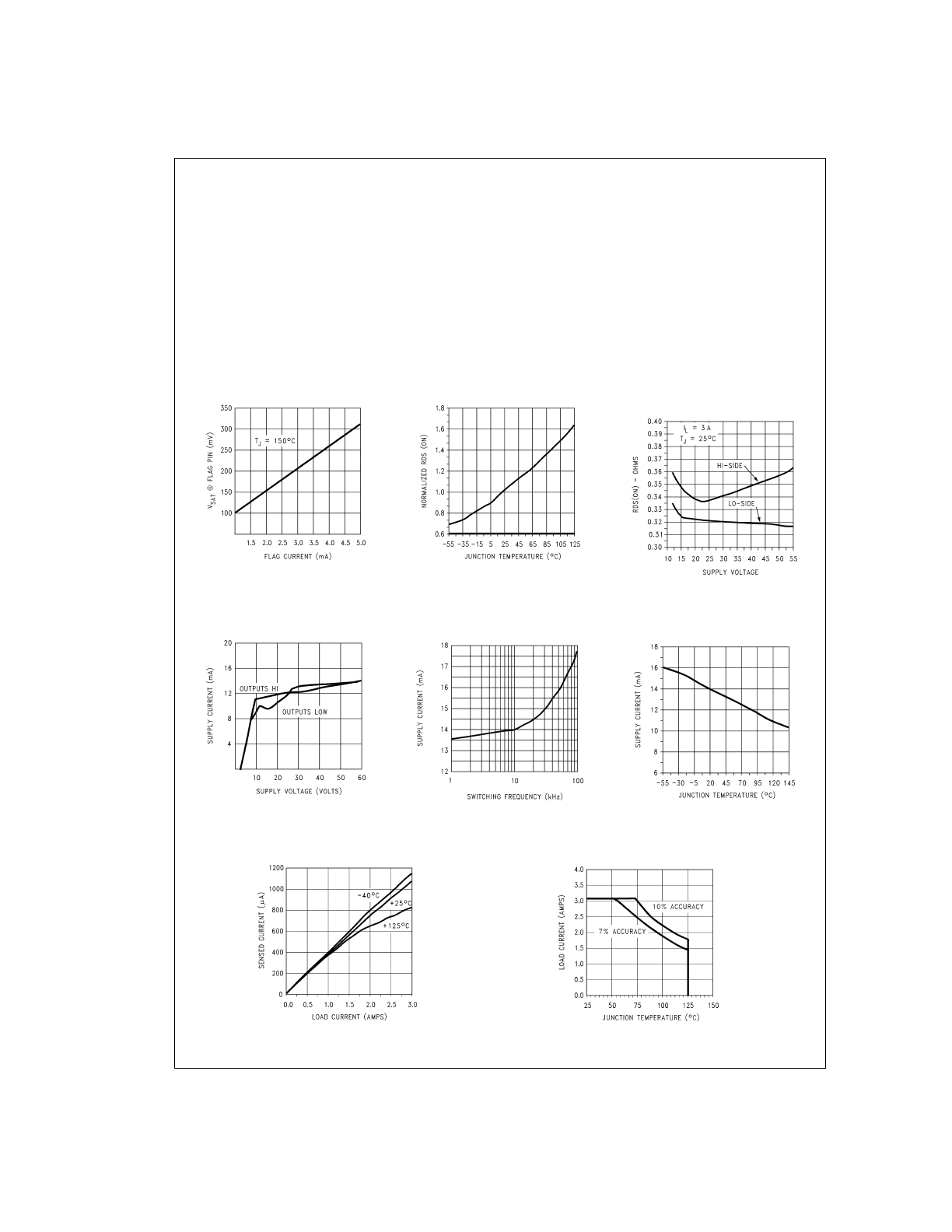
Typical Performance Characteristics
V
SAT
vs Flag Current
DS010568-16
R
DS
(ON) vs Temperature
DS010568-17
R
DS
(ON) vs
Supply Voltage
DS010568-18
Supply Current vs
Supply Voltage
DS010568-19
Supply Current vs
Frequency (V
S
= 42V)
DS010568-20
Supply Current vs
Temperature (V
S
= 42V)
DS010568-21
Current Sense Output
vs Load Current
DS010568-22
Current Sense
Operating Region
DS010568-23
www.national.com
4
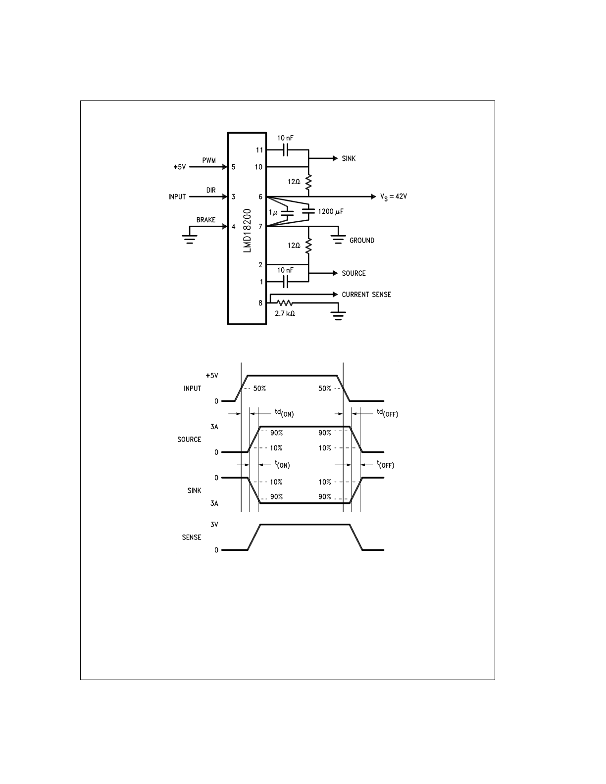
Test Circuit
Switching Time Definitions
Pinout Description
(See Connection Diagram)
Pin 1, BOOTSTRAP 1 Input: Bootstrap capacitor pin for half
H-bridge number 1. The recommended capacitor (10 nF) is
connected between pins 1 and 2.
Pin 2, OUTPUT 1: Half H-bridge number 1 output.
Pin 3, DIRECTION Input: See
Table 1
. This input controls
the direction of current flow between OUTPUT 1 and OUT-
PUT 2 (pins 2 and 10) and, therefore, the direction of rotation
of a motor load.
Pin 4, BRAKE Input: See
Table 1
. This input is used to
brake a motor by effectively shorting its terminals. When
braking is desired, this input is taken to a logic high level and
it is also necessary to apply logic high to PWM input, pin 5.
The drivers that short the motor are determined by the logic
level at the DIRECTION input (Pin 3): with Pin 3 logic high,
both current sourcing output transistors are ON; with Pin 3
logic low, both current sinking output transistors are ON. All
output transistors can be turned OFF by applying a logic high
to Pin 4 and a logic low to PWM input Pin 5; in this case only
a small bias current (approximately −1.5 mA) exists at each
output pin.
DS010568-8
DS010568-9
5
www.national.com
Pinout Description
(See Connection Diagram) (Continued)
Pin 5, PWM Input: See
Table 1
. How this input (and DIREC-
TION input, Pin 3) is used is determined by the format of the
PWM Signal.
Pin 6, V
S
Power Supply
Pin 7, GROUND Connection: This pin is the ground return,
and is internally connected to the mounting tab.
Pin 8, CURRENT SENSE Output: This pin provides the
sourcing current sensing output signal, which is typically
377 µA/A.
Pin 9, THERMAL FLAG Output: This pin provides the ther-
mal warning flag output signal. Pin 9 becomes active-low at
145˚C (junction temperature). However the chip will not shut
itself down until 170˚C is reached at the junction.
Pin 10, OUTPUT 2: Half H-bridge number 2 output.
Pin 11, BOOTSTRAP 2 Input: Bootstrap capacitor pin for
Half H-bridge number 2. The recommended capacitor
(10 nF) is connected between pins 10 and 11.
TABLE 1. Logic Truth Table
PWM
Dir
Brake
Active Output Drivers
H
H
L
Source 1, Sink 2
H
L
L
Sink 1, Source 2
L
X
L
Source 1, Source 2
H
H
H
Source 1, Source 2
H
L
H
Sink 1, Sink 2
L
X
H
NONE
Application Information
TYPES OF PWM SIGNALS
The LMD18200 readily interfaces with different forms of
PWM signals. Use of the part with two of the more popular
forms of PWM is described in the following paragraphs.
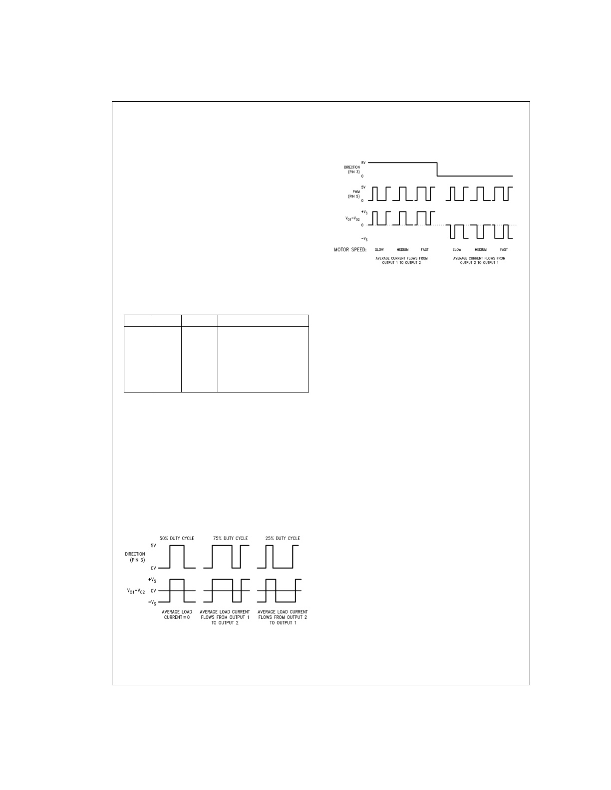
Simple, locked anti-phase PWM consists of a single, vari-
able duty-cycle signal in which is encoded both direction and
amplitude information (see
Figure 2
). A 50% duty-cycle
PWM signal represents zero drive, since the net value of
voltage (integrated over one period) delivered to the load is
zero. For the LMD18200, the PWM signal drives the direc-
tion input (pin 3) and the PWM input (pin 5) is tied to logic
high.
Sign/magnitude PWM consists of separate direction (sign)
and amplitude (magnitude) signals (see
Figure 3
). The (ab-
solute) magnitude signal is duty-cycle modulated, and the
absence of a pulse signal (a continuous logic low level) rep-
resents zero drive. Current delivered to the load is propor-
tional to pulse width. For the LMD18200, the DIRECTION in-
put (pin 3) is driven by the sign signal and the PWM input
(pin 5) is driven by the magnitude signal.
USING THE CURRENT SENSE OUTPUT
The CURRENT SENSE output (pin 8) has a sensitivity of
377 µA per ampere of output current. For optimal accuracy
and linearity of this signal, the value of voltage generating re-
sistor between pin 8 and ground should be chosen to limit
the maximum voltage developed at pin 8 to 5V, or less. The
maximum voltage compliance is 12V.
It should be noted that the recirculating currents (free wheel-
ing currents) are ignored by the current sense circuitry.
Therefore, only the currents in the upper sourcing outputs
are sensed.
USING THE THERMAL WARNING FLAG
The THERMAL FLAG output (pin 9) is an open collector tran-
sistor. This permits a wired OR connection of thermal warn-
ing flag outputs from multiple LMD18200’s, and allows the
user to set the logic high level of the output signal swing to
match system requirements. This output typically drives the
interrupt input of a system controller. The interrupt service
routine would then be designed to take appropriate steps,
such as reducing load currents or initiating an orderly system
shutdown. The maximum voltage compliance on the flag pin
is 12V.
SUPPLY BYPASSING
During switching transitions the levels of fast current
changes experienced may cause troublesome voltage tran-
sients across system stray inductance.
It is normally necessary to bypass the supply rail with a high
quality capacitor(s) connected as close as possible to the V
S
Power Supply (Pin 6) and GROUND (Pin 7). A 1 µF
high-frequency ceramic capacitor is recommended. Care
should be taken to limit the transients on the supply pin be-
low the Absolute Maximum Rating of the device. When oper-
ating the chip at supply voltages above 40V a voltage sup-
pressor (transorb) such as P6KE62A is recommended from
supply to ground. Typically the ceramic capacitor can be
eliminated in the presence of the voltage suppressor. Note
that when driving high load currents a greater amount of sup-
ply bypass capacitance (in general at least 100 µF per Amp
of load current) is required to absorb the recirculating cur-
rents of the inductive loads.
DS010568-4
FIGURE 2. Locked Anti-Phase PWM Control
DS010568-5
FIGURE 3. Sign/Magnitude PWM Control
www.national.com
6
Application Information
(Continued)
CURRENT LIMITING
Current limiting protection circuitry has been incorporated
into the design of the LMD18200. With any power device it is
important to consider the effects of the substantial surge cur-
rents through the device that may occur as a result of
shorted loads. The protection circuitry monitors this increase
in current (the threshold is set to approximately 10 Amps)
and shuts off the power device as quickly as possible in the
event of an overload condition. In a typical motor driving ap-
plication the most common overload faults are caused by
shorted motor windings and locked rotors. Under these con-
ditions the inductance of the motor (as well as any series in-
ductance in the V
CC
supply line) serves to reduce the mag-
nitude of a current surge to a safe level for the LMD18200.
Once the device is shut down, the control circuitry will peri-
odically try to turn the power device back on. This feature al-
lows the immediate return to normal operation in the event
that the fault condition has been removed. While the fault re-
mains however, the device will cycle in and out of thermal
shutdown. This can create voltage transients on the V
CC
supply line and therefore proper supply bypassing tech-
niques are required.
The most severe condition for any power device is a direct,
hard-wired (“screwdriver”) long term short from an output to
ground. This condition can generate a surge of current
through the power device on the order of 15 Amps and re-
quire the die and package to dissipate up to 500 Watts of
power for the short time required for the protection circuitry
to shut off the power device. This energy can be destructive,
particularly at higher operating voltages (
>
30V) so some
precautions are in order. Proper heat sink design is essential
and it is normally necessary to heat sink the V
CC
supply pin
(pin 6) with 1 square inch of copper on the PCB.
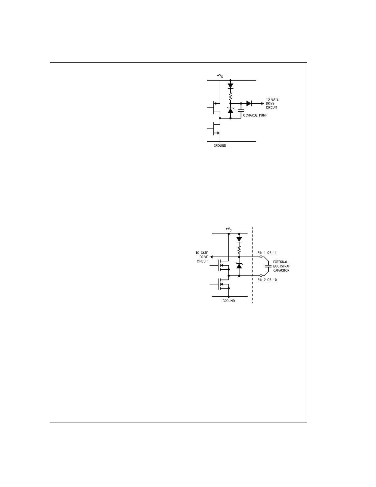
INTERNAL CHARGE PUMP AND USE OF BOOTSTRAP
CAPACITORS
To turn on the high-side (sourcing) DMOS power devices,
the gate of each device must be driven approximately 8V
more positive than the supply voltage. To achieve this an in-
ternal charge pump is used to provide the gate drive voltage.
As shown in
Figure 4
, an internal capacitor is alternately
switched to ground and charged to about 14V, then switched
to V supply thereby providing a gate drive voltage greater
than V supply. This switching action is controlled by a con-
tinuously running internal 300 kHz oscillator. The rise time of
this drive voltage is typically 20 µs which is suitable for oper-
ating frequencies up to 1 kHz.
For higher switching frequencies, the LMD18200 provides
for the use of external bootstrap capacitors. The bootstrap
principle is in essence a second charge pump whereby a
large value capacitor is used which has enough energy to
quickly charge the parasitic gate input capacitance of the
power device resulting in much faster rise times. The switch-
ing action is accomplished by the power switches them-
selves
Figure 5
. External 10 nF capacitors, connected from
the outputs to the bootstrap pins of each high-side switch
provide typically less than 100 ns rise times allowing switch-
ing frequencies up to 500 kHz.
INTERNAL PROTECTION DIODES
A major consideration when switching current through induc-
tive loads is protection of the switching power devices from
the large voltage transients that occur. Each of the four
switches in the LMD18200 have a built-in protection diode to
clamp transient voltages exceeding the positive supply or
ground to a safe diode voltage drop across the switch.
The reverse recovery characteristics of these diodes, once
the transient has subsided, is important. These diodes must
come out of conduction quickly and the power switches must
be able to conduct the additional reverse recovery current of
the diodes. The reverse recovery time of the diodes protect-
ing the sourcing power devices is typically only 70 ns with a
reverse recovery current of 1A when tested with a full 6A of
forward current through the diode. For the sinking devices
the recovery time is typically 100 ns with 4A of reverse cur-
rent under the same conditions.
DS010568-6
FIGURE 4. Internal Charge Pump Circuitry
DS010568-7
FIGURE 5. Bootstrap Circuitry
7
www.national.com
Typical Applications
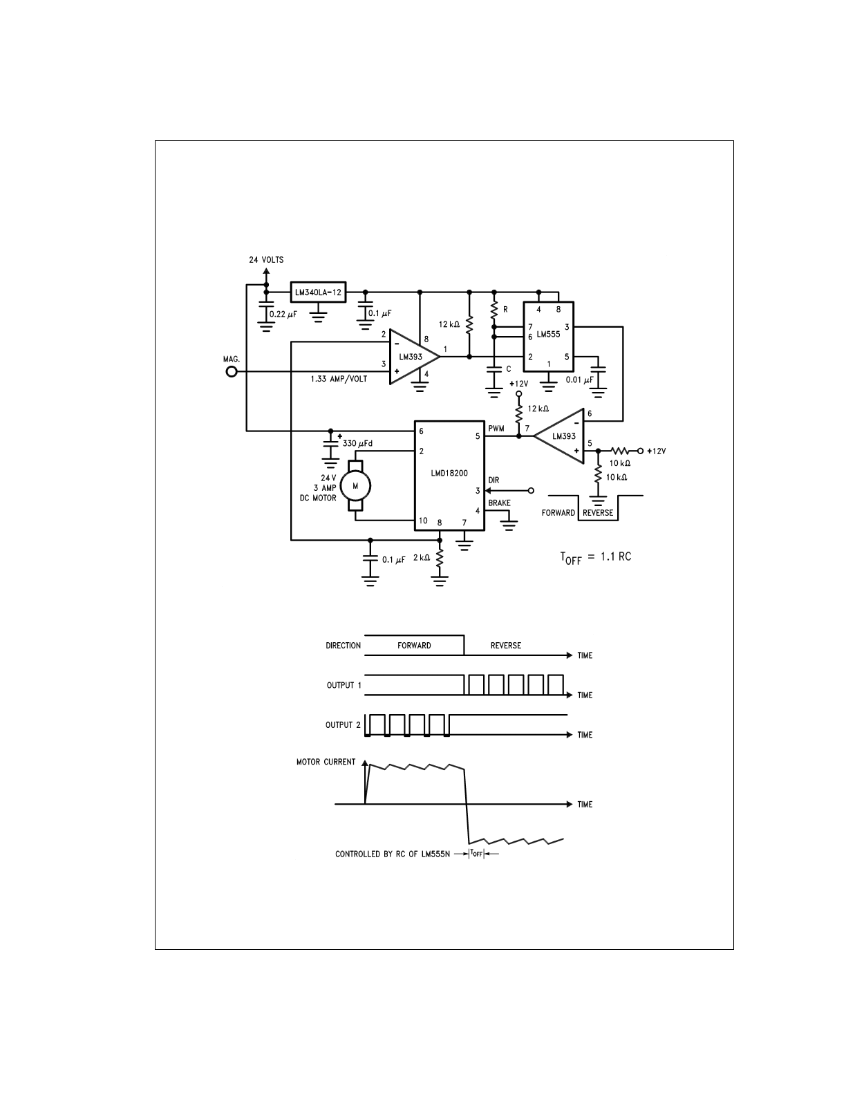
FIXED OFF-TIME CONTROL
This circuit controls the current through the motor by apply-
ing an average voltage equal to zero to the motor terminals
for a fixed period of time, whenever the current through the
motor exceeds the commanded current. This action causes
the motor current to vary slightly about an externally con-
trolled average level. The duration of the Off-period is ad-
justed by the resistor and capacitor combination of the
LM555. In this circuit the Sign/Magnitude mode of operation
is implemented (see Types of PWM Signals).
DS010568-10
FIGURE 6. Fixed Off-Time Control
DS010568-11
FIGURE 7. Switching Waveforms
www.national.com
8
Typical Applications
(Continued)
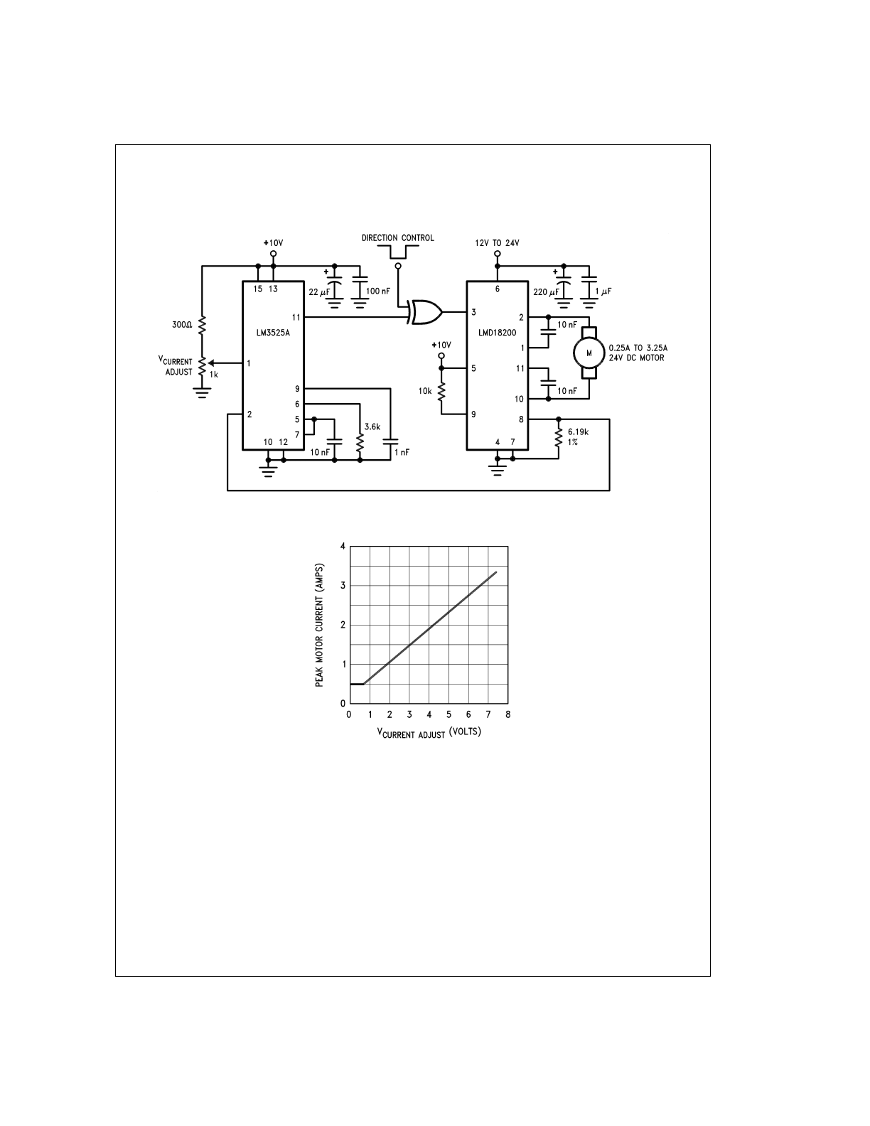
TORQUE REGULATION
Locked Anti-Phase Control of a brushed DC motor. Current sense output of the LMD18200 provides load sensing. The LM3525A
is a general purpose PWM controller. The relationship of peak motor current to adjustment voltage is shown in
Figure 9
.
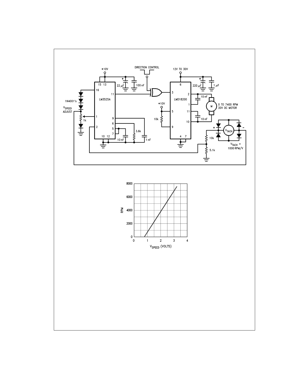
VELOCITY REGULATION
Utilizes tachometer output from the motor to sense motor speed for a locked anti-phase control loop. The relationship of motor
speed to the speed adjustment control voltage is shown in
Figure 11
.
DS010568-12
FIGURE 8. Locked Anti-Phase Control Regulates Torque
DS010568-13
FIGURE 9. Peak Motor Current
vs Adjustment Voltage
9
www.national.com
Typical Applications
(Continued)
DS010568-14
FIGURE 10. Regulate Velocity with Tachometer Feedback
DS010568-15
FIGURE 11. Motor Speed vs
Control Voltage
www.national.com
10

11
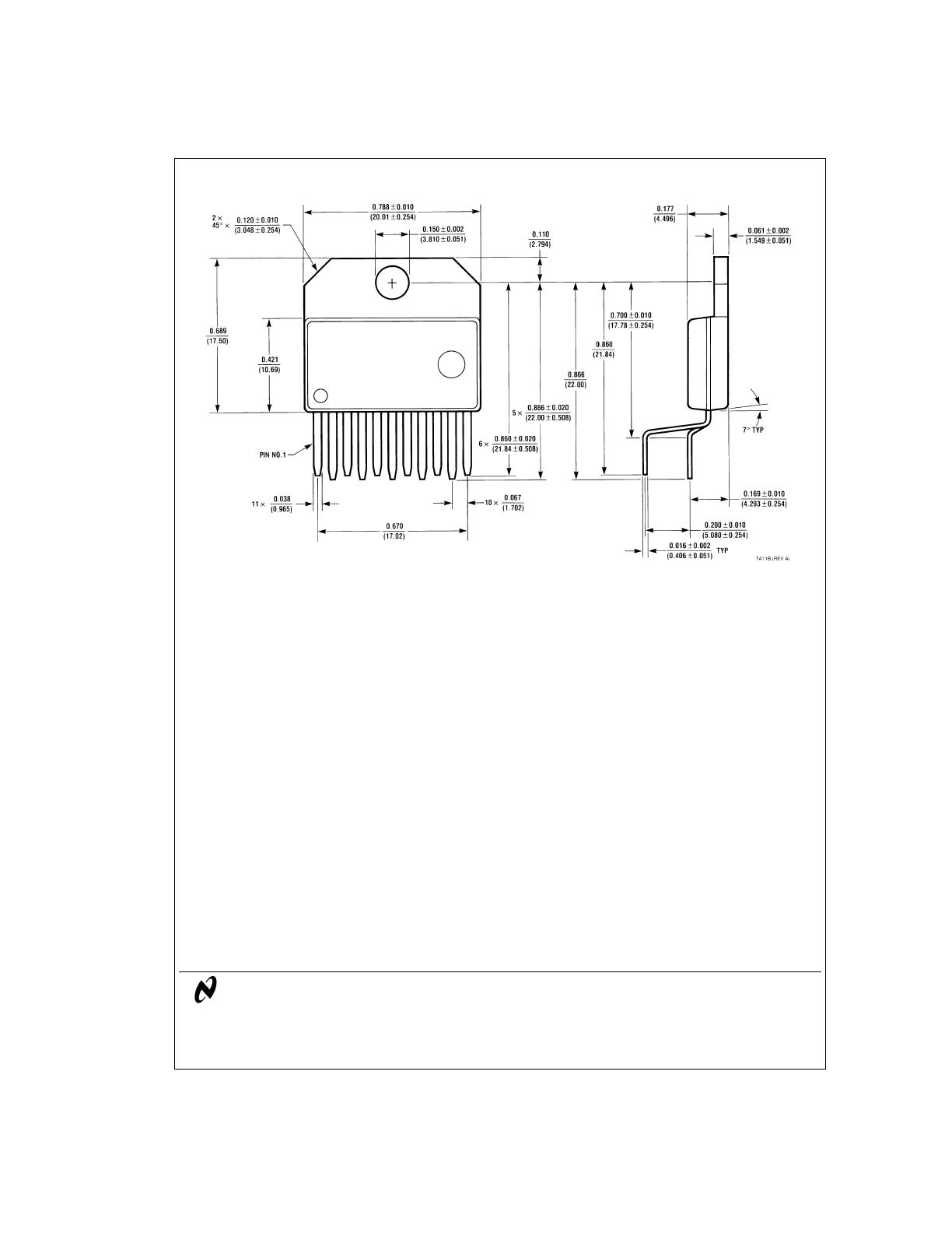
Physical Dimensions
inches (millimeters) unless otherwise noted
LIFE SUPPORT POLICY
NATIONAL’S PRODUCTS ARE NOT AUTHORIZED FOR USE AS CRITICAL COMPONENTS IN LIFE SUPPORT DE-
VICES OR SYSTEMS WITHOUT THE EXPRESS WRITTEN APPROVAL OF THE PRESIDENT OF NATIONAL SEMI-
CONDUCTOR CORPORATION. As used herein:
1. Life support devices or systems are devices or sys-
tems which, (a) are intended for surgical implant into
the body, or (b) support or sustain life, and whose fail-
ure to perform when properly used in accordance
with instructions for use provided in the labeling, can
be reasonably expected to result in a significant injury
to the user.
2. A critical component in any component of a life support
device or system whose failure to perform can be rea-
sonably expected to cause the failure of the life support
device or system, or to affect its safety or effectiveness.
National Semiconductor
Corporation
Americas
Tel: 1-800-272-9959
Fax: 1-800-737-7018
Email: support@nsc.com
www.national.com
National Semiconductor
Europe
Fax: +49 (0) 1 80-530 85 86
Email: europe.support@nsc.com
Deutsch Tel: +49 (0) 1 80-530 85 85
English
Tel: +49 (0) 1 80-532 78 32
Français Tel: +49 (0) 1 80-532 93 58
Italiano
Tel: +49 (0) 1 80-534 16 80
National Semiconductor
Asia Pacific Customer
Response Group
Tel: 65-2544466
Fax: 65-2504466
Email: sea.support@nsc.com
National Semiconductor
Japan Ltd.
Tel: 81-3-5620-6175
Fax: 81-3-5620-6179
11-Lead TO-220 Power Package (T)
Order Number LMD18200T
NS Package Number TA11B
LMD18200
3A,
55V
H-Bridge
National does not assume any responsibility for use of any circuitry described, no circuit patent licenses are implied and National reserves the right at any time without notice to change said circuitry and specifications.