
LM78S40
Universal Switching Regulator Subsystem
General Description
The LM78S40 is a monolithic regulator subsystem consisting
of all the active building blocks necessary for switching regu-
lator systems. The device consists of a temperature com-
pensated voltage reference, a duty-cycle controllable oscilla-
tor with an active current limit circuit, an error amplifier, high
current, high voltage output switch, a power diode and an
uncommitted operational amplifier. The device can drive ex-
ternal NPN or PNP transistors when currents in excess of
1.5A or voltages in excess of 40V are required. The device
can be used for step-down, step-up or inverting switching
regulators as well as for series pass regulators. It features
wide supply voltage range, low standby power dissipation,
high efficiency and low drift. It is useful for any stand-alone,
low part count switching system and works extremely well in
battery operated systems.
Features
n
Step-up, step-down or inverting switching regulators
n
Output adjustable from 1.25V to 40V
n
Peak currents to 1.5A without external transistors
n
Operation from 2.5V to 40V input
n
Low standby current drain
n
80 dB line and load regulation
n
High gain, high current, independent op amp
n
Pulse width modulation with no double pulsing
Block and Connection Diagrams
DS010057-2
16-Lead DIP
DS010057-1
Top View
April 1998
LM78S40
Universal
Switching
Regulator
Subsystem
© 1998 National Semiconductor Corporation
DS010057
www.national.com
Ordering Information
Part Number
NS Package
Temperature Range
LM78S40J/883
J16A Ceramic DIP
−55˚C to +125˚C
LM78S40N
N16E Molded DIP
−40˚C to +125˚C
LM78S40CN
N16E Molded DIP
0˚C to +70˚C
www.national.com
2
Absolute Maximum Ratings
(Note 1)
If Military/Aerospace specified devices are required,
please contact the National Semiconductor Sales Office/
Distributors for availability and specifications.
Storage Temperature Range
Ceramic DIP
−65˚C to +175˚C
Molded DIP
−65˚C to +150˚C
Operating Temperature Range
Extended (LM78S40J)
−55˚C to +125˚C
Industrial (LM78S40N)
−40˚C to +125˚C
Commercial (LM78S40CN)
0˚C to +70˚C
Lead Temperature
Ceramic DIP (Soldering, 60 sec.)
300˚C
Molded DIP (Soldering, 10 sec.)
265˚C
Internal Power Dissipation (Note 2) (Note 3)
16L-Ceramic DIP
1.50W
16L-Molded DIP
1.04W
Input Voltage from V
IN
to GND
40V
Input Voltage from V
+
(Op Amp)
to GND
40V
Common Mode Input Range
(Comparator and Op Amp)
−0.3 to V+
Differential Input Voltage
(Note 4)
±
30V
Output Short Circuit
Duration (Op Amp)
Continuous
Current from V
REF
10 mA
Voltage from Switch
Collectors to GND
40V
Voltage from Switch
Emitters to GND
40V
Voltage from Switch
Collectors to Emitter
40V
Voltage from Power Diode to GND
40V
Reverse Power Diode Voltage
40V
Current through Power Switch
1.5A
Current through Power Diode
1.5A
ESD Susceptibility
(to be determined)
LM78S40
Electrical Characteristics
(Note 5)
T
A
= Operating temperature range, V
IN
= 5.0V, V
+
(Op Amp) = 5.0V, unless otherwise specified.
Symbol
Parameter
Conditions
Min
Typ
Max
Units
GENERAL CHARACTERISTICS
I
CC
Supply Current
V
IN
= 5.0V
1.8
3.5
mA
(Op Amp Disconnected)
V
IN
= 40V
2.3
5.0
mA
I
CC
Supply Current
V
IN
= 5.0V
4.0
mA
(Op Amp Connected)
V
IN
= 40V
5.5
mA
REFERENCE SECTION
V
REF
Reference Voltage
I
REF
= 1.0 mA
Extend −55˚C
<
T
A
<
+125˚C,
Comm 0
<
T
A
<
+70˚C,
1.180
1.245
1.310
V
Indus −40˚C
<
T
A
<
+85˚C
V
R LINE
Reference Voltage
V
IN
= 3.0V to V
IN
= 40V,
0.04
0.2
mV/V
Line Regulation
I
REF
= 1.0 mA, T
A
= 25˚C
V
R LOAD
Reference Voltage
I
REF
= 1.0 mA to I
REF
= 10 mA,
0.2
0.5
mV/mA
Load Regulation
T
A
= 25˚C
OSCILLATOR SECTION
I
CHG
Charging Current
V
IN
= 5.0V, T
A
= 25˚C
20
50
µA
I
CHG
Charging Current
V
IN
= 40V, T
A
= 25˚C
20
70
µA
I
DISCHG
Discharge Current
V
IN
= 5.0V, T
A
= 25˚C
150
250
µA
I
DISCHG
Discharge Current
V
IN
= 40V, T
A
= 25˚C
150
350
µA
V
OSC
Oscillator Voltage Swing
V
IN
= 5.0V, T
A
= 25˚C
0.5
V
t
on
/t
off
Ratio of Charge/
6.0
µs/µs
Discharge Time
CURRENT LIMIT SECTION
V
CLS
Current Limit Sense
Voltage
T
A
= 25˚C
250
350
mV
OUTPUT SWITCH SECTION
V
SAT 1
Output Saturation Voltage 1
I
SW
= 1.0A (
Figure 1
)
1.1
1.3
V
V
SAT 2
Output Saturation Voltage 2
I
SW
= 1.0A (
Figure 2
)
0.45
0.7
V
3
www.national.com
LM78S40
Electrical Characteristics
(Note 5) (Continued)
T
A
= Operating temperature range, V
IN
= 5.0V, V
+
(Op Amp) = 5.0V, unless otherwise specified.
Symbol
Parameter
Conditions
Min
Typ
Max
Units
OUTPUT SWITCH SECTION
h
FE
Output Transistor Current
Gain
I
C
= 1.0A, V
CE
= 5.0V, T
A
= 25˚C
70
I
L
Output Leakage Current
V
O
= 40V, T
A
= 25˚C
10
nA
POWER DIODE
V
FD
Forward Voltage Drop
I
D
= 1.0A
1.25
1.5
V
I
DR
Diode Leakage Current
V
D
= 40V, T
A
= 25˚C
10
nA
COMPARATOR
V
IO
Input Offset Voltage
V
CM
= V
REF
1.5
15
mV
I
IB
Input Bias Current
V
CM
= V
REF
35
200
nA
I
IO
Input Offset Current
V
CM
= V
REF
5.0
75
nA
V
CM
Common Mode Voltage
Range
T
A
= 25˚C
0
V
IN
–2
V
PSRR
Power Supply Rejection
Ratio
V
IN
= 3.0V to 40V, T
A
= 25˚C
70
96
dB
OPERATIONAL AMPLIFIER
V
IO
Input Offset Voltage
V
CM
= 2.5V
4.0
15
mV
I
IB
Input Bias Current
V
CM
= 2.5V
30
200
nA
I
IO
Input Offset Current
V
CM
= 2.5V
5.0
75
nA
A
VS
+
Voltage Gain
+
R
L
= 2.0 k
Ω
to GND;
25
250
V/mV
V
O
= 1.0V to 2.5V, T
A
= 25˚C
A
VS
−
Voltage Gain
−
R
L
= 2.0 k
Ω
to V
+
(Op Amp)
25
250
V/mV
V
O
= 1.0V to 2.5V, T
A
= 25˚C
V
CM
Common Mode Voltage
Range
T
A
= 25˚C
0
V
CC
− 2
V
CMR
Common Mode Rejection
V
CM
= 0V to 3.0V, T
A
= 25˚C
76
100
dB
PSRR
Power Supply Rejection
Ratio
V
+
(Op Amp) = 3.0V to 40V, T
A
= 25˚C
76
100
dB
I
O
+
Output Source Current
T
A
= 25˚C
75
150
mA
I
O
−
Output Sink Current
T
A
= 25˚C
10
35
mA
SR
Slew Rate
T
A
= 25˚C
0.6
V/µs
V
OL
Output Voltage LOW
I
L
= −5.0 mA, T
A
= 25˚C
1.0
V
V
OH
Output Voltage High
I
L
= 50 mA, T
A
= 25˚C
V + (Op
V
Amp) −
3V
Note 1: Absolute Maximum Ratings indicate limits beyond which damage to the device may occur. Electrical specifications do not apply when ordering the device
beyond its rated operating conditions.
Note 2: T
J Max
= 150˚C for the Molded DIP, and 175˚C for the Ceramic DIP.
Note 3: Ratings apply to ambient temperature at 25˚C. Above this temperature, derate the 16L-Ceramic DIP at 10 mW/˚C, and the 16L-Molded DIP at 8.3 mW/˚C.
Note 4: For supply voltages less than 30V, the absolute maximum voltage is equal to the supply voltage.
Note 5: A military RETS specification is available on request. At the time of printing, the LM78S40 RETS specification complied with the Min and Max limits in this
table. The LM78S40J may also be procured as a Standard Military Drawing.
www.national.com
4
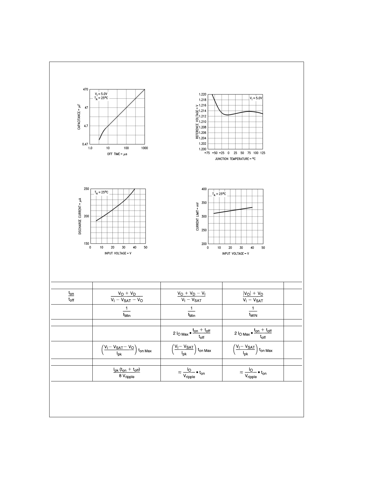
Typical Performance Characteristics
Design Formulas
Characteristic
Step-Down
Step-Up
Inverting
Units
(t
on
+ t
off
) Max
µs
C
T
4 x 10
−5
t
on
4 x 10
−5
t
on
4 x 10
−5
t
on
µF
I
pk
2 I
O Max
A
L
Min
µH
R
SC
0.33/I
pk
0.33/I
pk
0.33/I
pk
Ω
C
O
µF
Note 6: V
SAT
= Saturation voltage of the switching element.
V
D
= Forward voltage of the flyback diode.
C
T
vs OFF Time
DS010057-6
Reference Voltage vs
Junction Temperature
DS010057-7
Discharge Current vs
Input Voltage
DS010057-8
Current Limit Sense
Voltage vs Input Voltage
DS010057-9
5
www.national.com
Functional Description
SWITCHING FREQUENCY CONTROL
The LM78S40 is a variable frequency, variable duty cycle
device. The initial switching frequency is set by the timing
capacitor. (Oscillator frequency is set by a single external
capacitor and may be varied over a range of 100 Hz to
100 kHz). The initial duty cycle is 6:1. This switching fre-
quency and duty cycle can be modified by two
mechanisms — the current limit circuitry (I
pk sense
) and the
comparator.
The comparator modifies the OFF time. When the output
voltage is correct, the comparator output is in the HIGH
state and has no effect on the circuit operation. If the out-
put voltage is too high then the comparator output goes
LOW. In the LOW state the comparator inhibits the turn-on
of the output stage switching transistors. As long as the
comparator is LOW the system is in OFF time. As the out-
put current rises the OFF time decreases. As the output
current nears its maximum the OFF time approaches its
minimum value. The comparator can inhibit several ON
cycles, one ON cycle or any portion of an ON cycle. Once
the ON cycle has begun the comparator cannot inhibit un-
til the beginning of the next ON cycle.
The current limit modifies the ON time. The current limit is
activated when a 300 mV potential appears between lead
13 (V
CC
) and lead 14 (I
pk
). This potential is intended to re-
sult when designed for peak current flows through R
SC
.
When the peak current is reached the current limit is
turned on. The current limit circuitry provides for a quick
end to ON time and the immediate start of OFF time.
Generally the oscillator is free running but the current limit
action tends to reset the timing cycle.
Increasing load results in more current limited ON time
and less OFF time. The switching frequency increases
with load current.
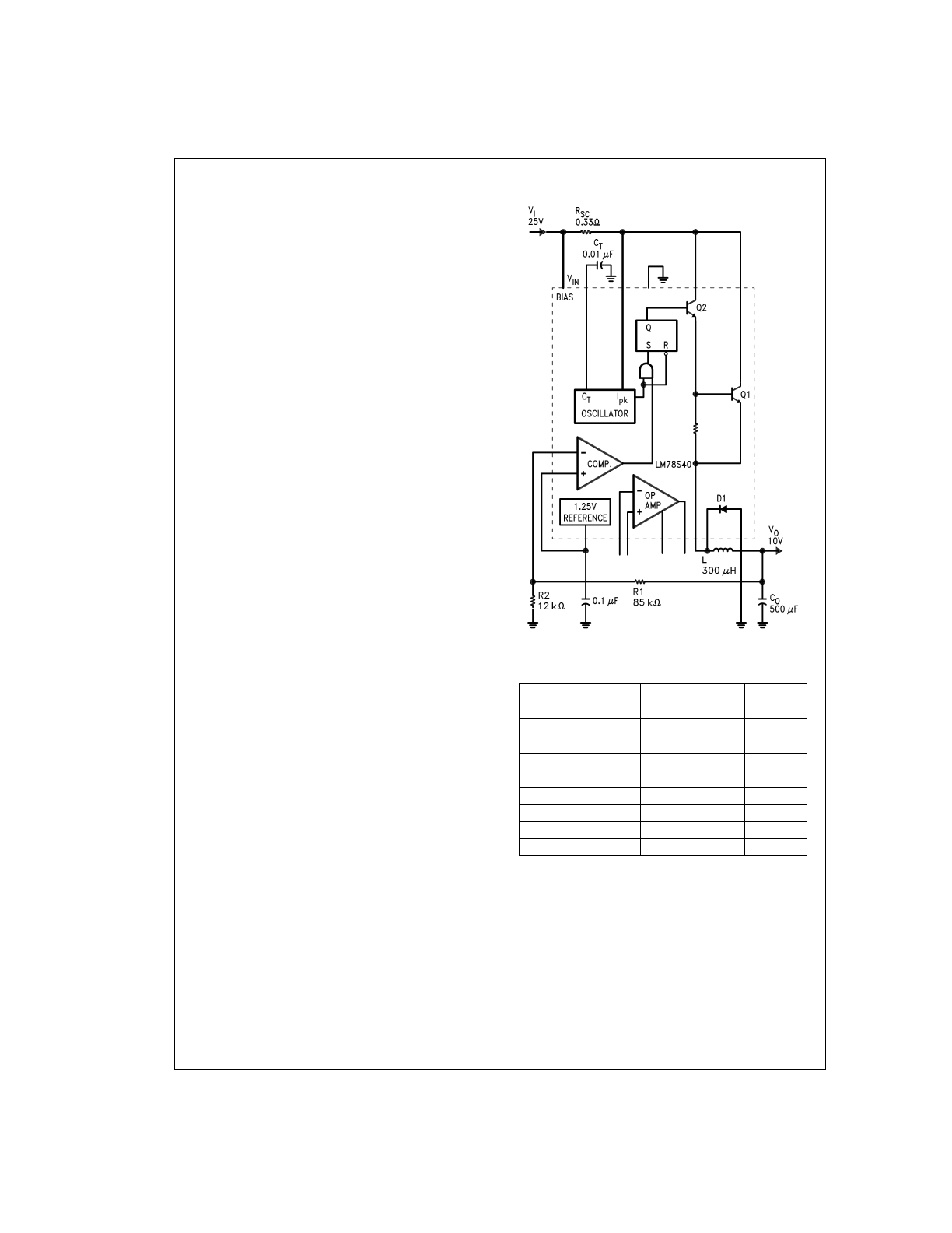
USING THE INTERNAL REFERENCE, DIODE, AND
SWITCH
The internal 1.245V reference (pin 8) must be bypassed,
with 0.1 µF directly to the ground pin (pin 11) of the
LM78S40, to assure its stability.
V
FD
is the forward voltage drop across the internal power
diode. It is listed on the data sheet as 1.25V typical, 1.5V
maximum. If an external diode is used, then its own for-
ward voltage drop must be used for V
FD
.
V
SAT
is the voltage across the switch element (output tran-
sistors Q1 and Q2) when the switch is closed or ON. This
is listed on the data sheet as Output Saturation Voltage.
“Output saturation voltage 1” is defined as the switching
element voltage for Q2 and Q1 in the Darlington configu-
ration with collectors tied together. This applies to
Figure
1
, the step down mode.
“Output saturation voltage 2” is the switching element volt-
age for Q1 only when used as a transistor switch. This ap-
plies to
Figure 2
, the step up mode.
For the inverting mode,
Figure 3
, the saturation voltage of
the external transistor should be used for V
SAT
.
Typical Applications
Characteristic
Condition
Typical
Value
Output Voltage
I
O
= 200 mA
10V
Line Regulation
20V
≤
V
I
≤
30V
1.5 mV
Load Regulation
5.0 mA
≤
I
O
3.0 mV
I
O
≤
300 mA
Max Output Current
V
O
= 9.5V
500 mA
Output Ripple
I
O
= 200 mA
50 mV
Efficiency
I
O
= 200 mA
74%
Standby Current
I
O
= 200 mA
2.8 mA
Note 7: For I
O
≥
200 mA use external diode to limit on-chip power
dissipation.
DS010057-3
FIGURE 1. Typical Step-Down Regulator and
Operational Performance (T
A
= 25˚C)
www.national.com
6
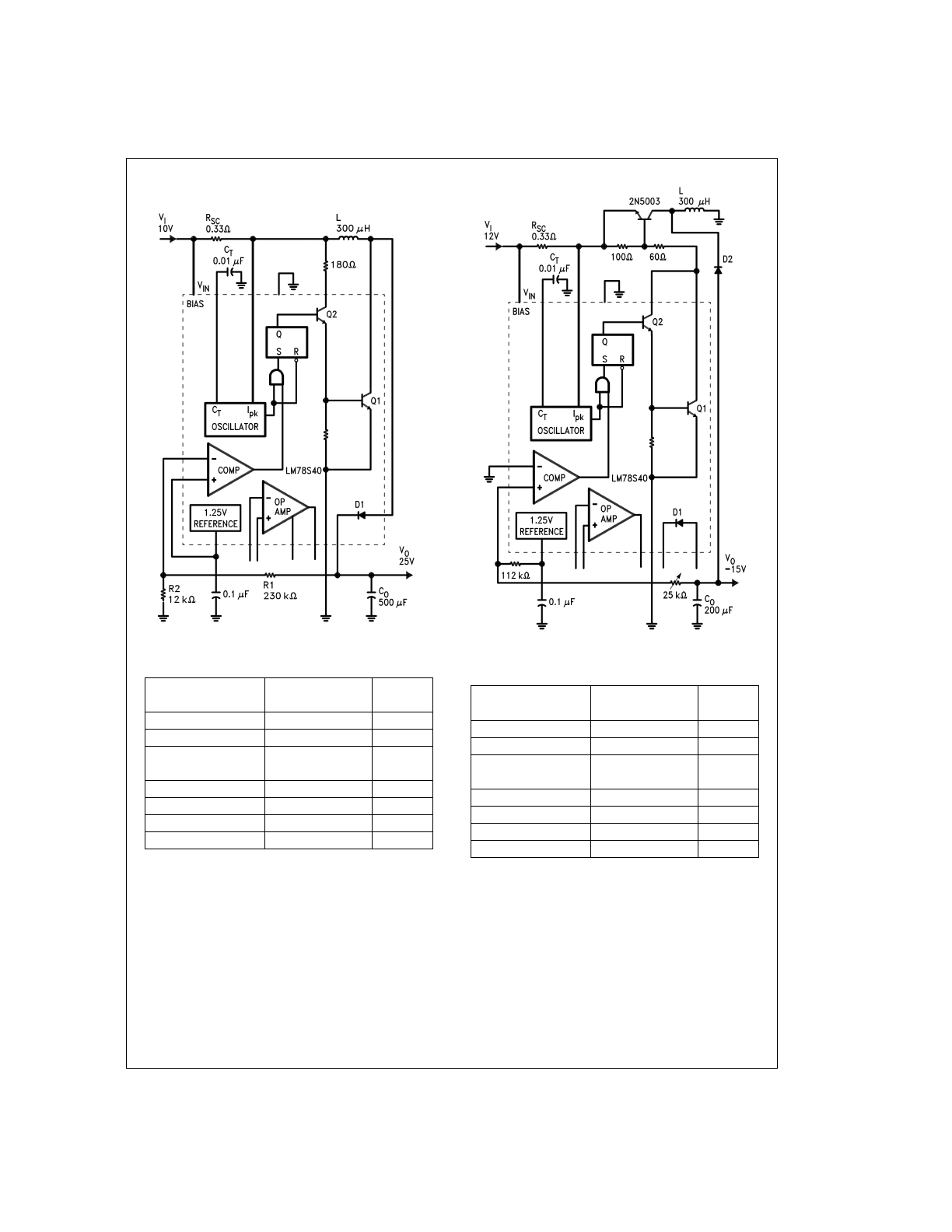
Typical Applications
(Continued)
Characteristic
Condition
Typical
Value
Output Voltage
I
O
= 50 mA
25V
Line Regulation
5.0V
≤
V
I
≤
15V
4.0 mV
Load Regulation
5.0 mA
≤
I
O
2.0 mV
I
O
≤
100 mA
Max Output Current
V
O
= 23.75V
160 mA
Output Ripple
I
O
= 50 mA
30 mV
Efficiency
I
O
= 50 mA
79%
Standby Current
I
O
= 50 mA
2.6 mA
Characteristic
Condition
Typical
Value
Output Voltage
I
O
= 100 mA
−15V
Line Regulation
8.0V
≤
V
I
≤
18V
5.0 mV
Load Regulation
5.0 mA
≤
I
O
3.0 mV
I
O
≤
150 mA
Max Output Current
V
O
= 14.25V
160 mA
Output Ripple
I
O
= 100 mA
20 mV
Efficiency
I
O
= 100 mA
70%
Standby Current
I
O
= 100 mA
2.3 mA
DS010057-4
FIGURE 2. Typical Step-Up Regulator and
Operational Performance (T
A
= 25˚C)
DS010057-5
FIGURE 3. Typical Inverting Regulator and
Operational Performance (T
A
= 25˚C)
7
www.national.com
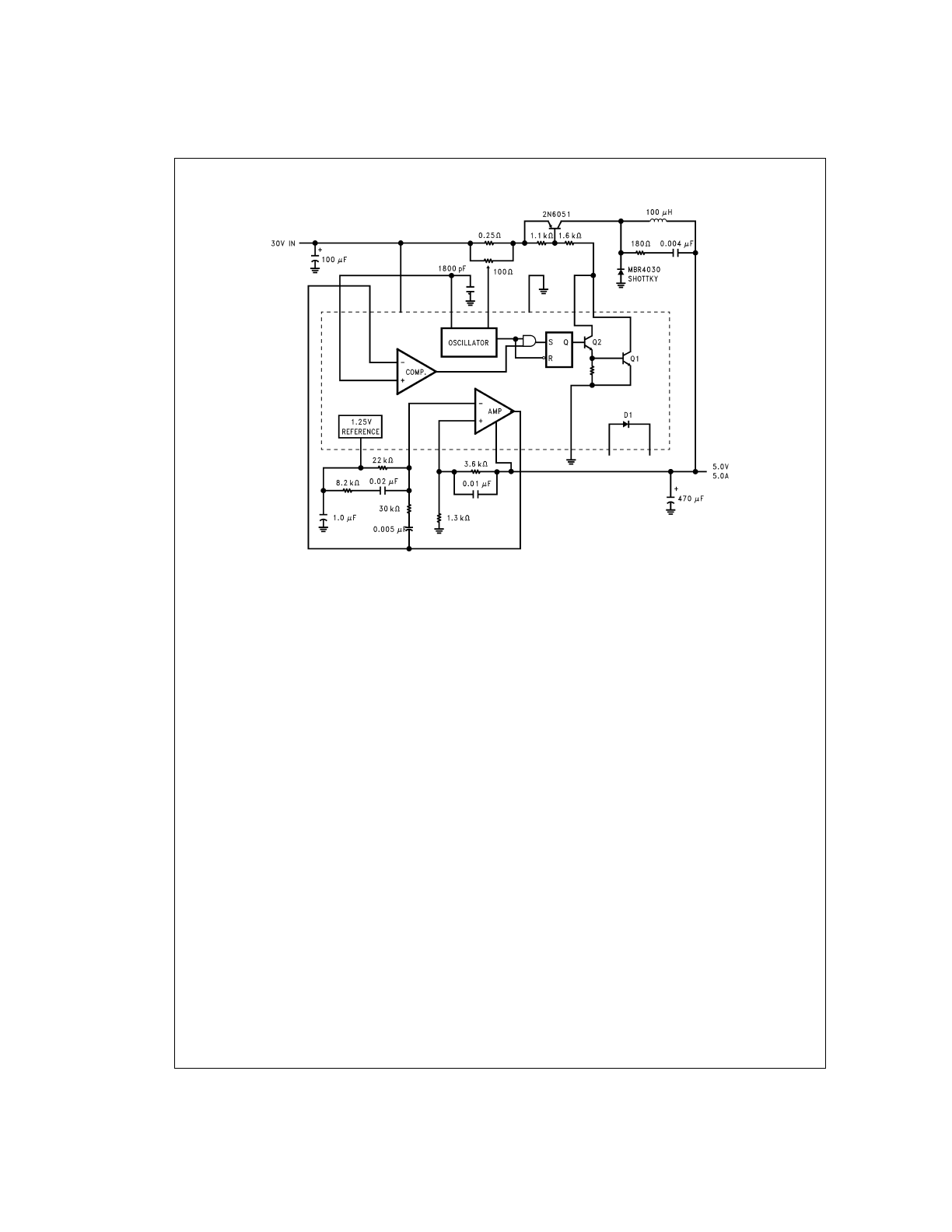
Typical Applications
(Continued)
DS010057-10
FIGURE 4. Pulse Width Modulated Step-Down Regulator (f
OSC
= 20 kHz)
www.national.com
8
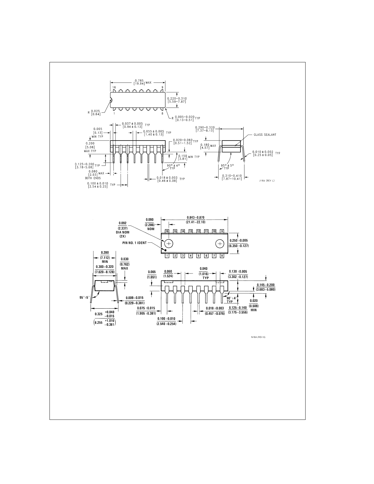
Physical Dimensions
inches (millimeters) unless otherwise noted
16-Lead Ceramic Dual-In-Line Package (J)
Order Number LM78S40J/883
NS Package Number J16A
16-Lead Molded Dual-In-Line Package (N)
Order Number LM78S40N or LM78S40CN
NS Package Number N16A
9
www.national.com
LIFE SUPPORT POLICY
NATIONAL’S PRODUCTS ARE NOT AUTHORIZED FOR USE AS CRITICAL COMPONENTS IN LIFE SUPPORT DE-
VICES OR SYSTEMS WITHOUT THE EXPRESS WRITTEN APPROVAL OF THE PRESIDENT OF NATIONAL SEMI-
CONDUCTOR CORPORATION. As used herein:
1. Life support devices or systems are devices or sys-
tems which, (a) are intended for surgical implant into
the body, or (b) support or sustain life, and whose fail-
ure to perform when properly used in accordance
with instructions for use provided in the labeling, can
be reasonably expected to result in a significant injury
to the user.
2. A critical component in any component of a life support
device or system whose failure to perform can be rea-
sonably expected to cause the failure of the life support
device or system, or to affect its safety or effectiveness.
National Semiconductor
Corporation
Americas
Tel: 1-800-272-9959
Fax: 1-800-737-7018
Email: support@nsc.com
www.national.com
National Semiconductor
Europe
Fax: +49 (0) 1 80-530 85 86
Email: europe.support@nsc.com
Deutsch Tel: +49 (0) 1 80-530 85 85
English
Tel: +49 (0) 1 80-532 78 32
Français Tel: +49 (0) 1 80-532 93 58
Italiano
Tel: +49 (0) 1 80-534 16 80
National Semiconductor
Asia Pacific Customer
Response Group
Tel: 65-2544466
Fax: 65-2504466
Email: sea.support@nsc.com
National Semiconductor
Japan Ltd.
Tel: 81-3-5620-6175
Fax: 81-3-5620-6179
LM78S40
Universal
Switching
Regulator
Subsystem
National does not assume any responsibility for use of any circuitry described, no circuit patent licenses are implied and National reserves the right at any time without notice to change said circuitry and specifications.