
TL/H/7746
LM78XX
Series
Voltage
Regulators
February 1995
LM78XX Series Voltage Regulators
General Description
The LM78XX series of three terminal regulators is available
with several fixed output voltages making them useful in a
wide range of applications. One of these is local on card
regulation, eliminating the distribution problems associated
with single point regulation. The voltages available allow
these regulators to be used in logic systems, instrumenta-
tion, HiFi, and other solid state electronic equipment. Al-
though designed primarily as fixed voltage regulators these
devices can be used with external components to obtain
adjustable voltages and currents.
The LM78XX series is available in an aluminum TO-3 pack-
age which will allow over 1.0A load current if adequate heat
sinking is provided. Current limiting is included to limit the
peak output current to a safe value. Safe area protection for
the output transistor is provided to limit internal power dissi-
pation. If internal power dissipation becomes too high for
the heat sinking provided, the thermal shutdown circuit
takes over preventing the IC from overheating.
Considerable effort was expanded to make the LM78XX se-
ries of regulators easy to use and mininize the number
of external components. It is not necessary to bypass the
output, although this does improve transient response. Input
bypassing is needed only if the regulator is located far from
the filter capacitor of the power supply.
For output voltage other than 5V, 12V and 15V the LM117
series provides an output voltage range from 1.2V to 57V.
Features
Y
Output current in excess of 1A
Y
Internal thermal overload protection
Y
No external components required
Y
Output transistor safe area protection
Y
Internal short circuit current limit
Y
Available in the aluminum TO-3 package
Voltage Range
LM7805C
5V
LM7812C
12V
LM7815C
15V
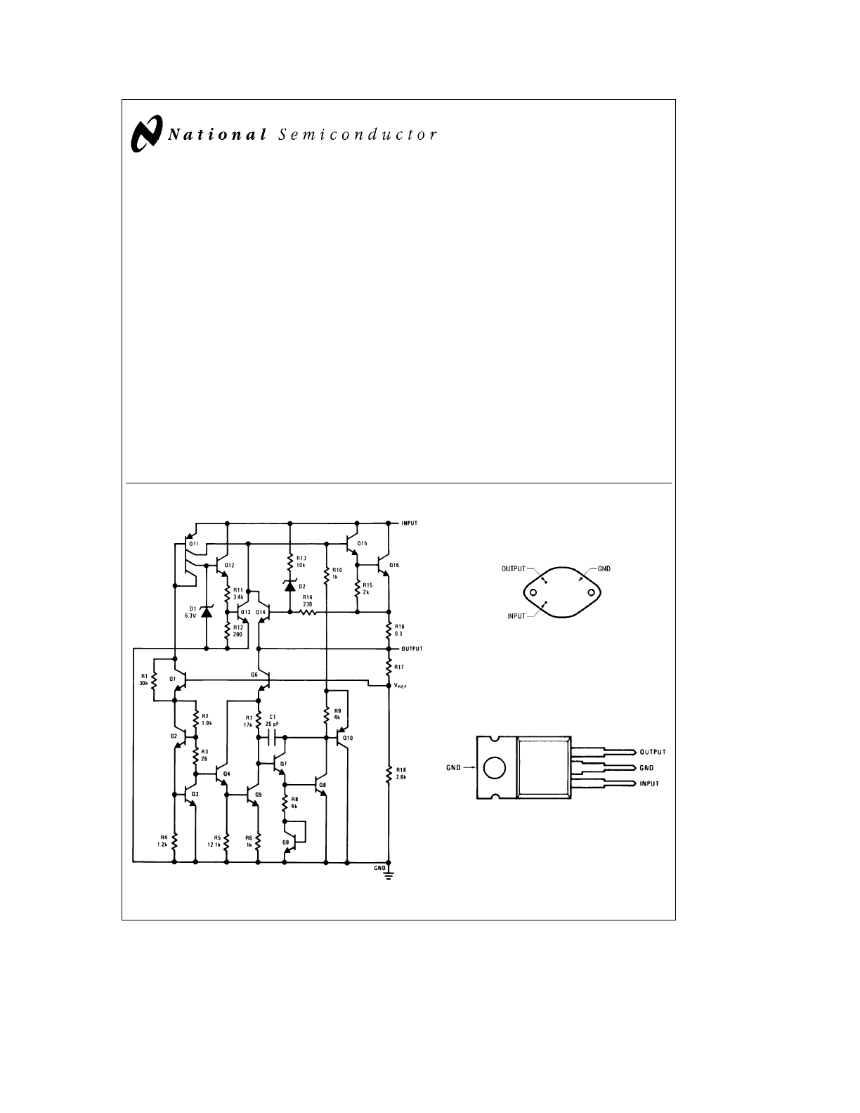
Schematic and Connection Diagrams
TL/H/7746 – 1
Metal Can Package
TO-3 (K)
Aluminum
TL/H/7746 – 2
Bottom View
Order Number LM7805CK,
LM7812CK or LM7815CK
See NS Package Number KC02A
Plastic Package
TO-220 (T)
TL/H/7746 – 3
Top View
Order Number LM7805CT,
LM7812CT or LM7815CT
See NS Package Number T03B
C1995 National Semiconductor Corporation
RRD-B30M115/Printed in U. S. A.
Absolute Maximum Ratings
If Military/Aerospace specified devices are required,
please contact the National Semiconductor Sales
Office/Distributors for availability and specifications.
Input Voltage (V
O
e
5V, 12V and 15V)
35V
Internal Power Dissipation (Note 1)
Internally Limited
Operating Temperature Range (T
A
)
0
§
C to
a
70
§
C
Maximum Junction Temperature
(K Package)
150
§
C
(T Package)
150
§
C
Storage Temperature Range
b
65
§
C to
a
150
§
C
Lead Temperature (Soldering, 10 sec.)
TO-3 Package K
300
§
C
TO-220 Package T
230
§
C
Electrical Characteristics LM78XXC
(Note 2) 0
§
C
s
Tj
s
125
§
C unless otherwise noted.
Output Voltage
5V
12V
15V
Input Voltage (unless otherwise noted)
10V
19V
23V
Units
Symbol
Parameter
Conditions
Min
Typ
Max
Min
Typ
Max
Min
Typ
Max
V
O
Output Voltage
Tj
e
25
§
C, 5 mA
s
I
O
s
1A
4.8
5
5.2
11.5
12
12.5
14.4
15
15.6
V
P
D
s
15W, 5 mA
s
I
O
s
1A
4.75
5.25
11.4
12.6 14.25
15.75
V
V
MIN
s
V
IN
s
V
MAX
(7.5
s
V
IN
s
20)
(14.5
s
V
IN
s
27)
(17.5
s
V
IN
s
30)
V
D
V
O
Line Regulation
I
O
e
500 mA Tj
e
25
§
C
3
50
4
120
4
150
mV
D
V
IN
(7
s
V
IN
s
25)
14.5
s
V
IN
s
30)
(17.5
s
V
IN
s
30)
V
0
§
C
s
Tj
s
a
125
§
C
50
120
150
mV
D
V
IN
(8
s
V
IN
s
20)
(15
s
V
IN
s
27)
(18.5
s
V
IN
s
30)
V
I
O
s
1A
Tj
e
25
§
C
50
120
150
mV
D
V
IN
(7.5
s
V
IN
s
20)
(14.6
s
V
IN
s
27)
(17.7
s
V
IN
s
30)
V
0
§
C
s
Tj
s
a
125
§
C
25
60
75
mV
D
V
IN
(8
s
V
IN
s
12)
(16
s
V
IN
s
22)
(20
s
V
IN
s
26)
V
D
V
O
Load Regulation
Tj
e
25
§
C
5 mA
s
I
O
s
1.5A
10
50
12
120
12
150
mV
250 mA
s
I
O
s
750 mA
25
60
75
mV
5 mA
s
I
O
s
1A, 0
§
C
s
Tj
s
a
125
§
C
50
120
150
mV
I
Q
Quiescent Current
I
O
s
1A
Tj
e
25
§
C
8
8
8
mA
0
§
C
s
Tj
s
a
125
§
C
8.5
8.5
8.5
mA
D
I
Q
Quiescent Current
5 mA
s
I
O
s
1A
0.5
0.5
0.5
mA
Change
Tj
e
25
§
C, I
O
s
1A
1.0
1.0
1.0
mA
V
MIN
s
V
IN
s
V
MAX
(7.5
s
V
IN
s
20)
(14.8
s
V
IN
s
27)
(17.9
s
V
IN
s
30)
V
I
O
s
500 mA, 0
§
C
s
Tj
s
a
125
§
C
1.0
1.0
1.0
mA
V
MIN
s
V
IN
s
V
MAX
(7
s
V
IN
s
25)
(14.5
s
V
IN
s
30)
(17.5
s
V
IN
s
30)
V
V
N
Output Noise Voltage T
A
e
25
§
C, 10 Hz
s
f
s
100 kHz
40
75
90
m
V
D
V
IN
D
V
OUT
Ripple Rejection
I
O
s
1A, Tj
e
25
§
C or
62
80
55
72
54
70
dB
f
e
120 Hz
I
O
s
500 mA
62
55
54
dB
Ð
0
§
C
s
Tj
s
a
125
§
C
V
MIN
s
V
IN
s
V
MAX
(8
s
V
IN
s
18)
(15
s
V
IN
s
25)
(18.5
s
V
IN
s
28.5)
V
R
O
Dropout Voltage
Tj
e
25
§
C, I
OUT
e
1A
2.0
2.0
2.0
V
Output Resistance
f
e
1 kHz
8
18
19
mX
Short-Circuit Current Tj
e
25
§
C
2.1
1.5
1.2
A
Peak Output Current Tj
e
25
§
C
2.4
2.4
2.4
A
Average TC of V
OUT
0
§
C
s
Tj
s
a
125
§
C, I
O
e
5 mA
0.6
1.5
1.8
mV/
§
C
V
IN
Input Voltage
Required to Maintain Tj
e
25
§
C, I
O
s
1A
7.5
14.6
17.7
V
Line Regulation
Note 1:
Thermal resistance of the TO-3 package (K, KC) is typically 4
§
C/W junction to case and 35
§
C/W case to ambient. Thermal resistance of the TO-220
package (T) is typically 4
§
C/W junction to case and 50
§
C/W case to ambient.
Note 2:
All characteristics are measured with capacitor across the input of 0.22 mF, and a capacitor across the output of 0.1mF. All characteristics except noise
voltage and ripple rejection ratio are measured using pulse techniques (t
w
s
10 ms, duty cycle
s
5%). Output voltage changes due to changes in internal
temperature must be taken into account separately.
2
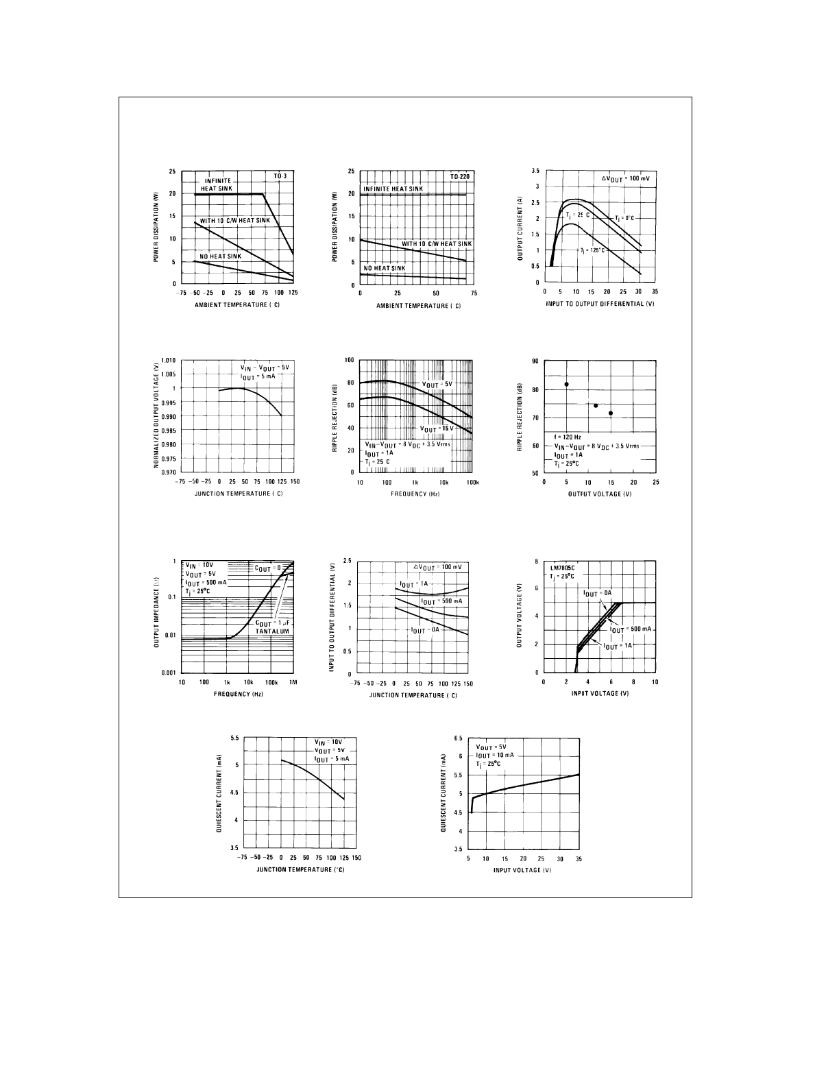
Typical Performance Characteristics
Dissipation
Maximum Average Power
Dissipation
Maximum Average Power
Peak Output Current
to 1V at Tj
e
25
§
C)
Output Voltage (Normalized
Ripple Rejection
Ripple Rejection
Output Impedance
Dropout Voltage
Dropout Characteristics
Quiescent Current
Quiescent Current
TL/H/7746 – 4
3

4
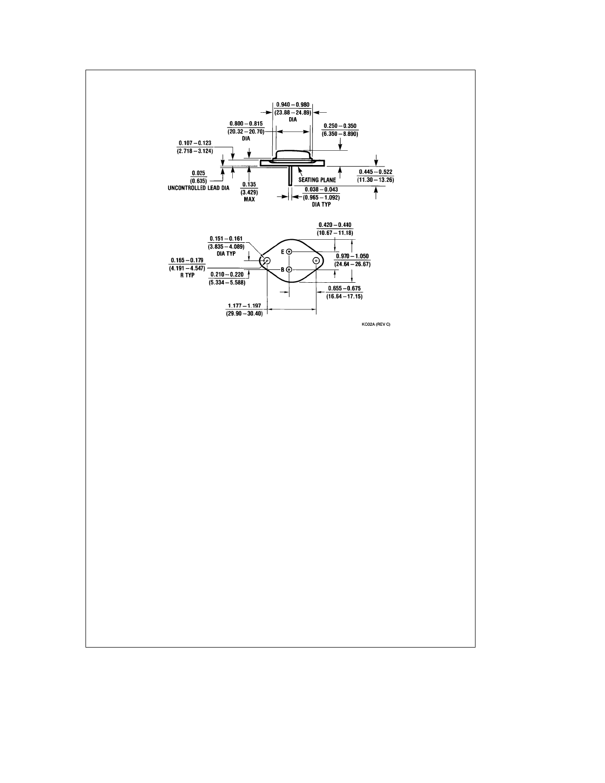
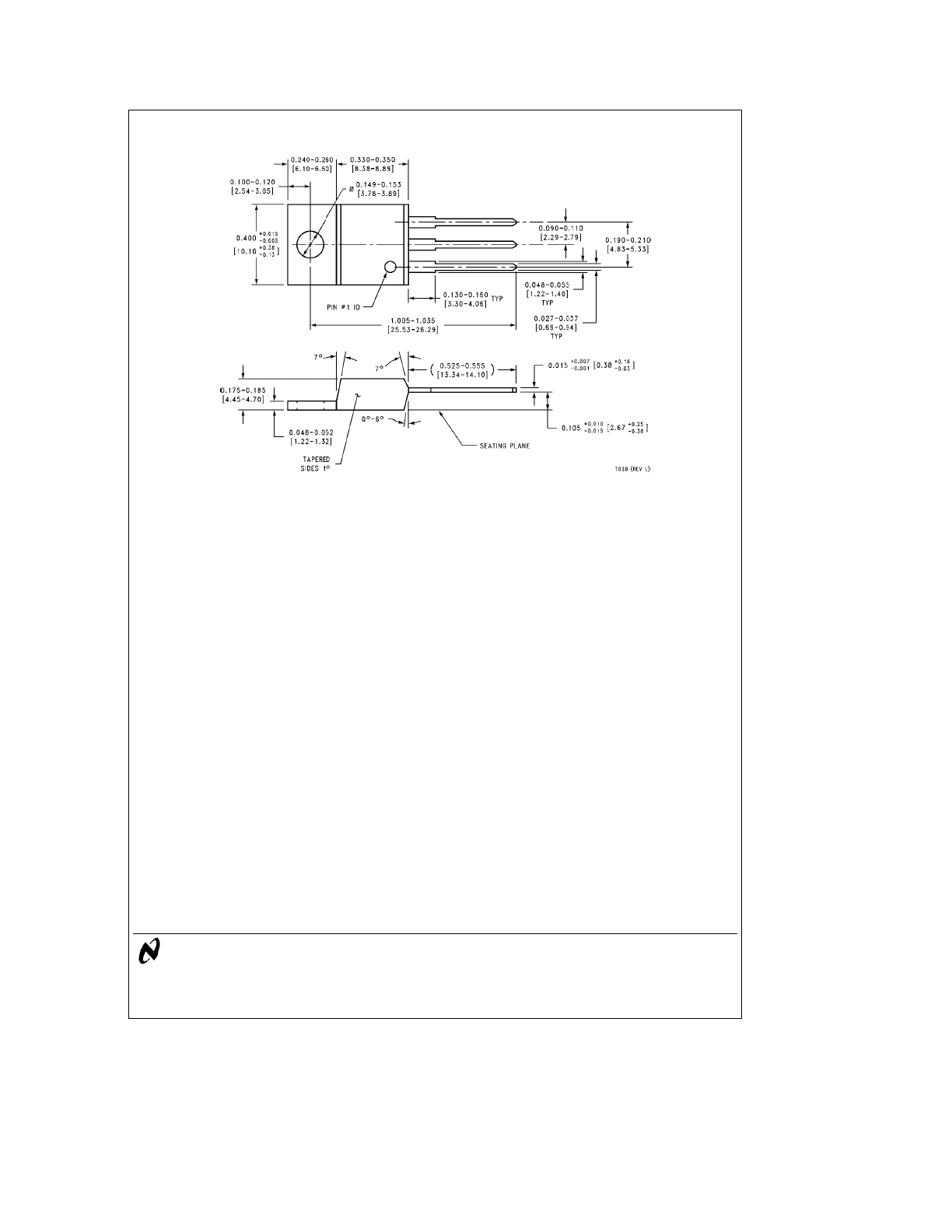
Physical Dimensions
inches (millimeters)
Aluminum Metal Can Package (KC)
Order Number LM7805CK, LM7812CK or LM7815CK
NS Package Number KC02A
5
LM78XX
Series
Voltage
Regulators
Physical Dimensions
inches (millimeters) (Continued)
TO-220 Package (T)
Order Number LM7805CT, LM7812CT or LM7815CT
NS Package Number T03B
LIFE SUPPORT POLICY
NATIONAL’S PRODUCTS ARE NOT AUTHORIZED FOR USE AS CRITICAL COMPONENTS IN LIFE SUPPORT
DEVICES OR SYSTEMS WITHOUT THE EXPRESS WRITTEN APPROVAL OF THE PRESIDENT OF NATIONAL
SEMICONDUCTOR CORPORATION. As used herein:
1. Life support devices or systems are devices or
2. A critical component is any component of a life
systems which, (a) are intended for surgical implant
support device or system whose failure to perform can
into the body, or (b) support or sustain life, and whose
be reasonably expected to cause the failure of the life
failure to perform, when properly used in accordance
support device or system, or to affect its safety or
with instructions for use provided in the labeling, can
effectiveness.
be reasonably expected to result in a significant injury
to the user.
National Semiconductor
National Semiconductor
National Semiconductor
National Semiconductor
Corporation
Europe
Hong Kong Ltd.
Japan Ltd.
1111 West Bardin Road
Fax: (
a
49) 0-180-530 85 86
13th Floor, Straight Block,
Tel: 81-043-299-2309
Arlington, TX 76017
Email: cnjwge
@
tevm2.nsc.com
Ocean Centre, 5 Canton Rd.
Fax: 81-043-299-2408
Tel: 1(800) 272-9959
Deutsch Tel: (
a
49) 0-180-530 85 85
Tsimshatsui, Kowloon
Fax: 1(800) 737-7018
English
Tel: (
a
49) 0-180-532 78 32
Hong Kong
Fran
3ais Tel: (
a
49) 0-180-532 93 58
Tel: (852) 2737-1600
Italiano
Tel: (
a
49) 0-180-534 16 80
Fax: (852) 2736-9960
National does not assume any responsibility for use of any circuitry described, no circuit patent licenses are implied and National reserves the right at any time without notice to change said circuitry and specifications.