
TL/H/10484
LM341
LM78MXX
Series
3-Terminal
Positive
Voltage
Regulators
January 1995
LM341, LM78MXX Series
3-Terminal Positive Voltage Regulators
General Description
The LM341 and LM78MXX series of three-terminal positive
voltage regulators employ built-in current limiting, thermal
shutdown, and safe-operating area protection which makes
them virtually immune to damage from output overloads.
With adequate heatsinking, they can deliver in excess of
0.5A output current. Typical applications would include local
(on-card) regulators which can eliminate the noise and de-
graded performance associated with single-point regulation.
Features
Y
Output current in excess of 0.5A
Y
No external components
Y
Internal thermal overload protection
Y
Internal short circuit current-limiting
Y
Output transistor safe-area compensation
Y
Available in TO-220 and TO-39 packages
Y
Output voltages of 5V, 12V, and 15V
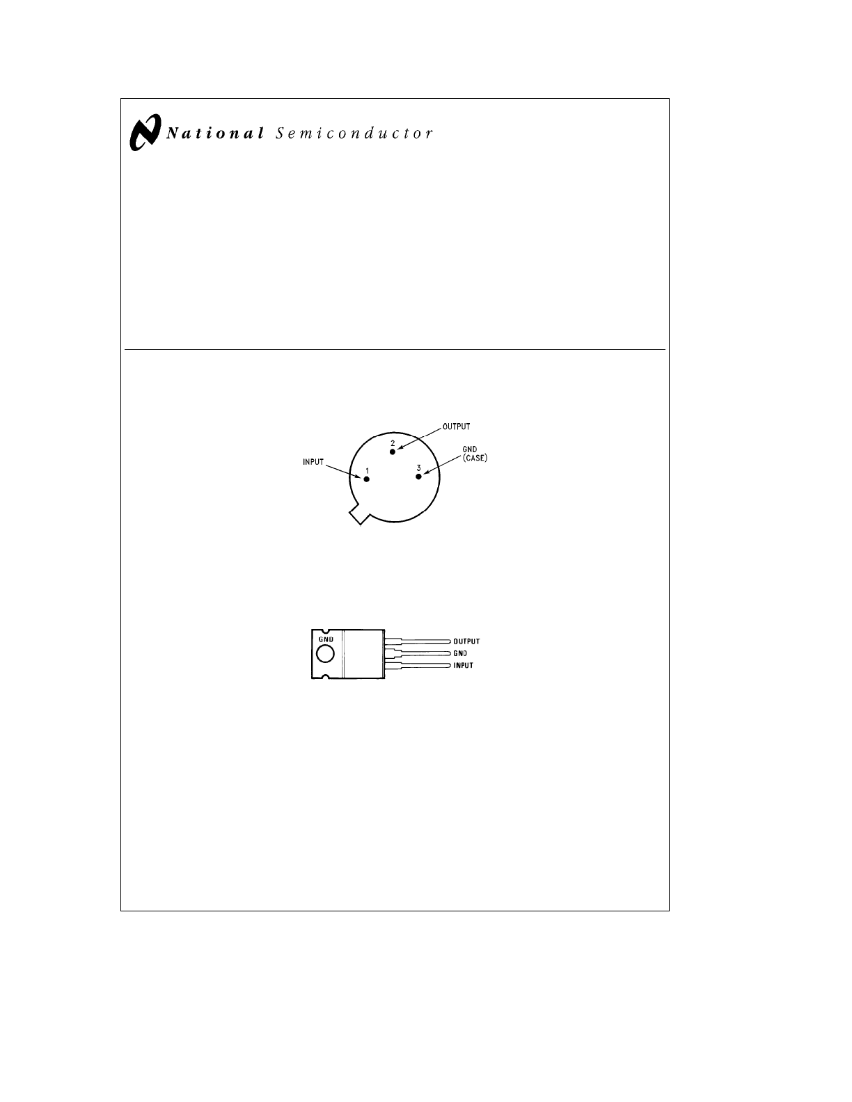
Connection Diagrams
TO-39 Metal Can Package (H)
TL/H/10484 – 5
Bottom View
Order Number LM78M05CH, LM78M12CH or LM78M15CH
See NS Package Number H03A
TO-220 Power Package (T)
TL/H/10484 – 6
Top View
Order Number LM341T-5.0, LM341T-12 or LM341T-15
See NS Package Number T03B
C1995 National Semiconductor Corporation
RRD-B30M115/Printed in U. S. A.
Absolute Maximum Ratings
(Note 1)
If Military/Aerospace specified devices are required,
please contact the National Semiconductor Sales
Office/Distributors for availability and specifications.
Lead Temperature (Soldering, 10 seconds)
TO-39 Package (H)
300
§
C
TO-220 Package (T)
260
§
C
Storage Temperature Range
b
65
§
C to
a
150
§
C
Operating Junction Temperature Range
b
40
§
C to
a
125
§
C
Power Dissipation (Note 2)
Internally Limited
Input Voltage
5V
s
V
O
s
15V
35V
ESD Susceptibility
TBD
Electrical Characteristics
Limits in standard typeface are for T
J
e
25
§
C, and limits in boldface type apply over the
b
40
§
C to
a
125
§
C operating
temperature range. Limits are guaranteed by production testing or correlation techniques using standard Statistical Quality
Control (SQC) methods.
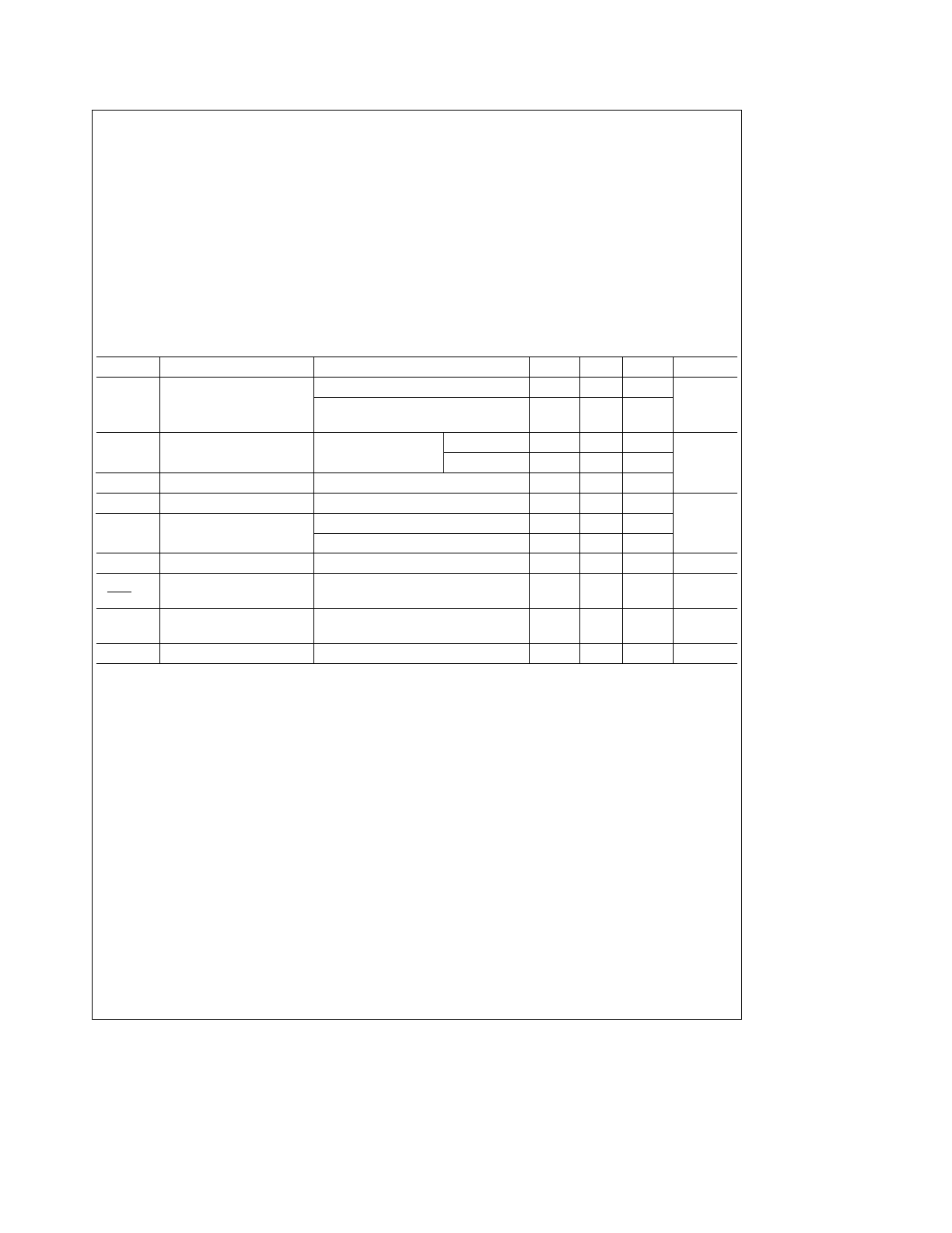
LM341-5.0, LM78M05C
Unless otherwise specified: V
IN
e
10V, C
IN
e
0.33 mF, C
O
e
0.1 mF
Symbol
Parameter
Conditions
Min
Typ
Max
Units
V
O
Output Voltage
I
L
e
500 mA
4.8
5.0
5.2
V
5 mA
s
I
L
s
500 mA
4.75
5.0
5.25
P
D
s
7.5W, 7.5V
s
V
IN
s
20V
V
R LINE
Line Regulation
7.2V
s
V
IN
s
25V
I
L
e
100 mA
50
mV
I
L
e
500 mA
100
V
R LOAD
Load Regulation
5 mA
s
I
L
s
500 mA
100
I
Q
Quiescent Current
I
L
e
500 mA
4
10.0
mA
D
I
Q
Quiescent Current Change
5 mA
s
I
L
s
500 mA
0.5
7.5V
s
V
IN
s
25V, I
L
e
500 mA
1.0
V
n
Output Noise Voltage
f
e
10 Hz to 100 kHz
40
m
V
D
V
IN
D
V
O
Ripple Rejection
f
e
120 Hz, I
L
e
500 mA
78
dB
V
IN
Input Voltage Required
I
L
e
500 mA
7.2
V
to Maintain Line Regulation
D
V
O
Long Term Stability
I
L
e
500 mA
20
mV/khrs
2
Electrical Characteristics
Limits in standard typeface are for T
J
e
25
§
C, and limits in boldface type apply over the
b
40
§
C to
a
125
§
C operating
temperature range. Limits are guaranteed by production testing or correlation techniques using standard Statistical Quality
Control (SQC) methods. (Continued)
LM341-12, LM78M12C
Unless otherwise specified: V
IN
e
19V, C
IN
e
0.33 mF, C
O
e
0.1 mF
Symbol
Parameter
Conditions
Min
Typ
Max
Units
V
O
Output Voltage
I
L
e
500 mA
11.5
12
12.5
V
5 mA
s
I
L
s
500 mA
11.4
12
12.6
P
D
s
7.5W, 14.8V
s
V
IN
s
27V
V
R LINE
Line Regulation
14.5V
s
V
IN
s
30V
I
L
e
100 mA
120
mV
I
L
e
500 mA
240
V
R LOAD
Load Regulation
5 mA
s
I
L
s
500 mA
240
I
Q
Quiescent Current
I
L
e
500 mA
4
10.0
mA
D
I
Q
Quiescent Current Change
5 mA
s
I
L
s
500 mA
0.5
14.8V
s
V
IN
s
30V, I
L
e
500 mA
1.0
V
n
Output Noise Voltage
f
e
10 Hz to 100 kHz
75
m
V
D
V
IN
D
V
O
Ripple Rejection
f
e
120 Hz, I
L
e
500 mA
71
dB
V
IN
Input Voltage Required
I
L
e
500 mA
14.5
V
to Maintain Line Regulation
D
V
O
Long Term Stability
I
L
e
500 mA
48
mV/khrs
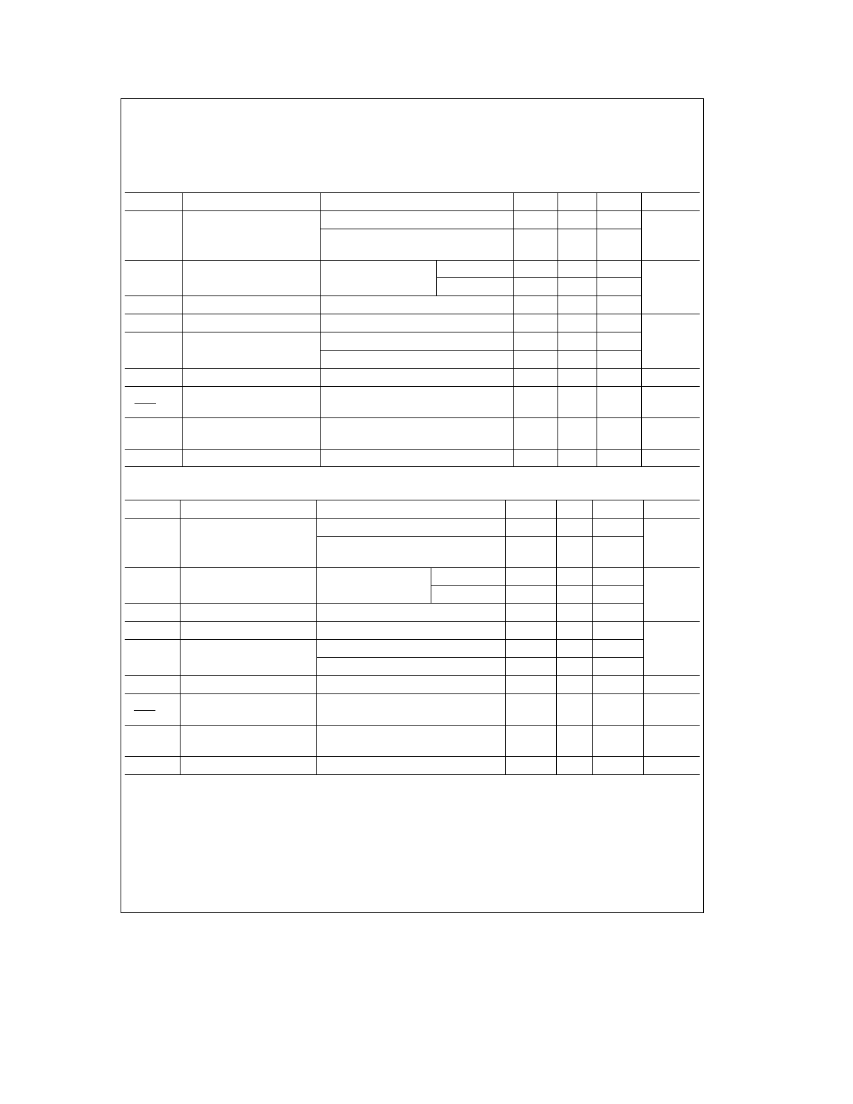
LM341-15, LM78M15C
Unless otherwise specified: V
IN
e
23V, C
IN
e
0.33 mF, C
O
e
0.1 mF
Symbol
Parameter
Conditions
Min
Typ
Max
Units
V
O
Output Voltage
I
L
e
500 mA
14.4
15
15.6
V
5 mA
s
I
L
s
500 mA
14.25
15
15.75
P
D
s
7.5W, 18V
s
V
IN
s
30V
V
R LINE
Line Regulation
17.6V
s
V
IN
s
30V
I
L
e
100 mA
150
mV
I
L
e
500 mA
300
V
R LOAD
Load Regulation
5 mA
s
I
L
s
500 mA
300
I
Q
Quiescent Current
I
L
e
500 mA
4
10.0
mA
D
I
Q
Quiescent Current Change
5 mA
s
I
L
s
500 mA
0.5
18V
s
V
IN
s
30V, I
L
e
500 mA
1.0
V
n
Output Noise Voltage
f
e
10 Hz to 100 kHz
90
m
V
D
V
IN
D
V
O
Ripple Rejection
f
e
120 Hz, I
L
e
500 mA
69
dB
V
IN
Input Voltage Required
I
L
e
500 mA
17.6
V
to Maintain Line Regulation
D
V
O
Long Term Stability
I
L
e
500 mA
60
mV/khrs
Note 1:
Absolute maximum ratings indicate limits beyond which damage to the component may occur. Electrical specifications do not apply when operating the
device outside of its rated operating conditions.
Note 2:
The typical thermal resistance of the three package types is:
T
(TO-220) package: i
(J-A)
e
60
§
C/W, i
(J-C
) e 5
§
C/W
H
(TO-39) package: i
(J-A)
e
120
§
C/W, i
(J-C
) e 18
§
C/W
3
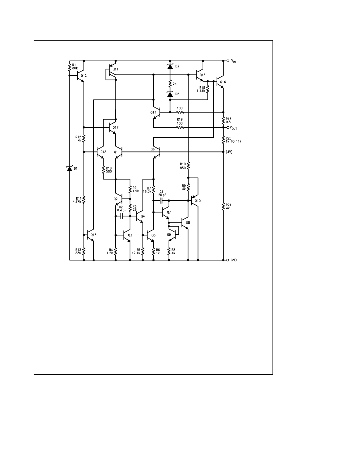
Schematic Diagram
TL/H/10484 – 1
4
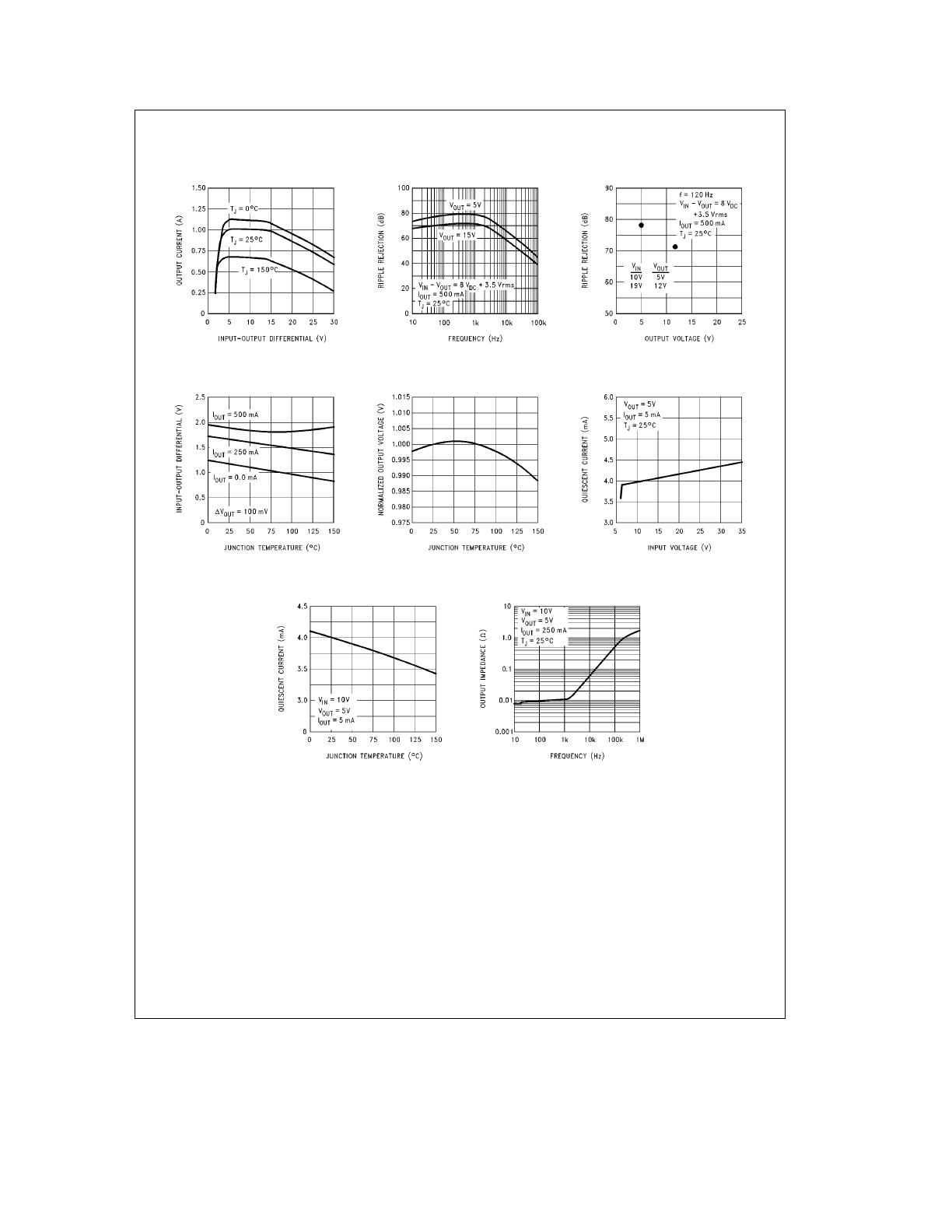
Typical Performance Characteristics
Peak Output Current
Ripple Rejection
Ripple Rejection
Dropout Voltage
to 1V at T
J
e
25
§
C)
Output Voltage (Normalized
Quiescent Current
Quiescent Current
Output Impedance
TL/H/10484 – 4
5
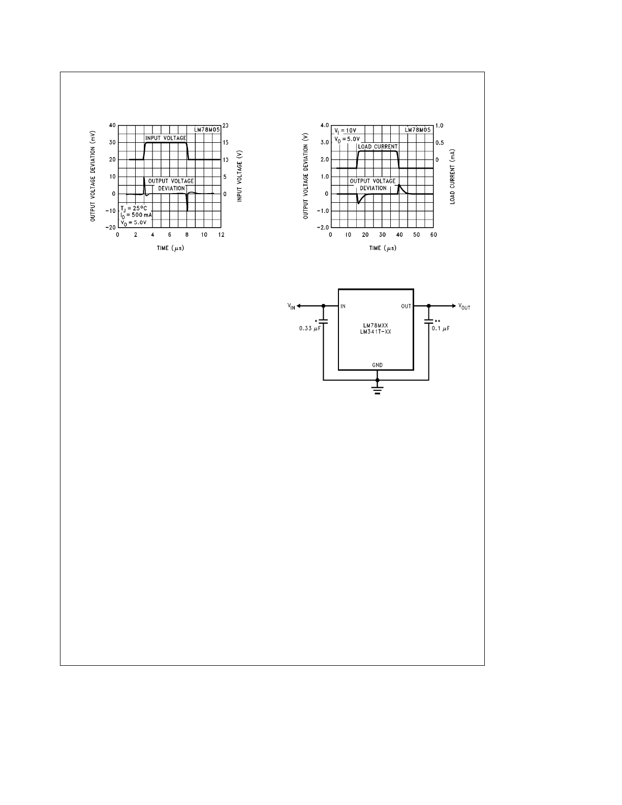
Typical Performance Characteristics
(Continued)
Line Transient Response
TL/H/10484 – 7
Load Transient Response
TL/H/10484 – 8
Design Considerations
The LM78MXX/LM341XX fixed voltage regulator series has
built-in thermal overload protection which prevents the de-
vice from being damaged due to excessive junction temper-
ature.
The regulators also contain internal short-circuit protection
which limits the maximum output current, and safe-area pro-
tection for the pass transistor which reduces the short-cir-
cuit current as the voltage across the pass transistor is in-
creased.
Although the internal power dissipation is automatically lim-
ited, the maximum junction temperature of the device must
be kept below
a
125
§
C in order to meet data sheet specifi-
cations. An adequate heatsink should be provided to assure
this limit is not exceeded under worst-case operating condi-
tions (maximum input voltage and load current) if reliable
performance is to be obtained.
Typical Application
TL/H/10484 – 9
*Required if regulator input is more than 4 inches from input filter capacitor
(or if no input filter capacitor is used).
**Optional for improved transient response.
6
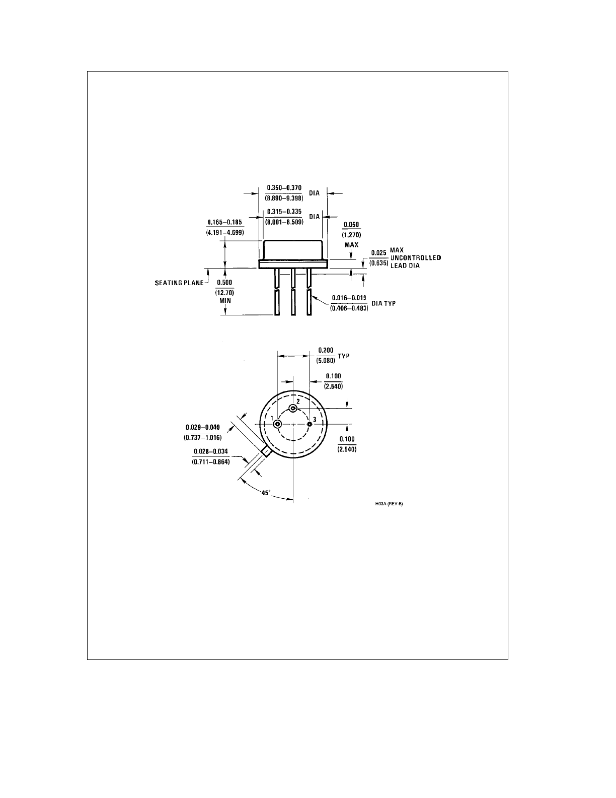
Physical Dimensions
inches (millimeters)
TO-39 Metal Can Package (H)
Order Number LM78M05CH, LM78M12CH or LM78M15CH
NS Package Number H03A
7
LM341
LM78MXX
Series
3-Terminal
Positive
Voltage
Regulators
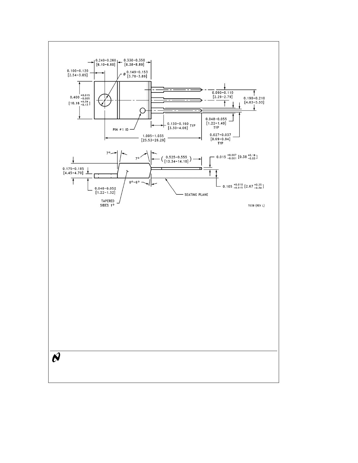
Physical Dimensions
inches (millimeters) (Continued)
TO-220 Power Package (T)
Order Number LM341T-5.0, LM341T-12 or LM341T-15
NS Package Number T03B
LIFE SUPPORT POLICY
NATIONAL’S PRODUCTS ARE NOT AUTHORIZED FOR USE AS CRITICAL COMPONENTS IN LIFE SUPPORT
DEVICES OR SYSTEMS WITHOUT THE EXPRESS WRITTEN APPROVAL OF THE PRESIDENT OF NATIONAL
SEMICONDUCTOR CORPORATION. As used herein:
1. Life support devices or systems are devices or
2. A critical component is any component of a life
systems which, (a) are intended for surgical implant
support device or system whose failure to perform can
into the body, or (b) support or sustain life, and whose
be reasonably expected to cause the failure of the life
failure to perform, when properly used in accordance
support device or system, or to affect its safety or
with instructions for use provided in the labeling, can
effectiveness.
be reasonably expected to result in a significant injury
to the user.
National Semiconductor
National Semiconductor
National Semiconductor
National Semiconductor
Corporation
Europe
Hong Kong Ltd.
Japan Ltd.
1111 West Bardin Road
Fax: (
a
49) 0-180-530 85 86
13th Floor, Straight Block,
Tel: 81-043-299-2309
Arlington, TX 76017
Email: cnjwge
@
tevm2.nsc.com
Ocean Centre, 5 Canton Rd.
Fax: 81-043-299-2408
Tel: 1(800) 272-9959
Deutsch Tel: (
a
49) 0-180-530 85 85
Tsimshatsui, Kowloon
Fax: 1(800) 737-7018
English
Tel: (
a
49) 0-180-532 78 32
Hong Kong
Fran
3ais Tel: (
a
49) 0-180-532 93 58
Tel: (852) 2737-1600
Italiano
Tel: (
a
49) 0-180-534 16 80
Fax: (852) 2736-9960
National does not assume any responsibility for use of any circuitry described, no circuit patent licenses are implied and National reserves the right at any time without notice to change said circuitry and specifications.