
TL/H/9064
LM317L
3-Terminal
Adjustable
Regulator
February 1995
LM317L 3-Terminal Adjustable Regulator
General Description
The LM317L is an adjustable 3-terminal positive voltage
regulator capable of supplying 100 mA over a 1.2V to 37V
output range. It is exceptionally easy to use and requires
only two external resistors to set the output voltage. Further,
both line and load regulation are better than standard fixed
regulators. Also, the LM317L is available packaged in a
standard TO-92 transistor package which is easy to use.
In addition to higher performance than fixed regulators, the
LM317L offers full overload protection. Included on the chip
are current limit, thermal overload protection and safe area
protection. All overload protection circuitry remains fully
functional even if the adjustment terminal is disconnected.
Features
Y
Adjustable output down to 1.2V
Y
Guaranteed 100 mA output current
Y
Line regulation typically 0.01%V
Y
Load regulation typically 0.1%
Y
Current limit constant with temperature
Y
Eliminates the need to stock many voltages
Y
Standard 3-lead transistor package
Y
80 dB ripple rejection
Y
Output is short circuit protected
Normally, no capacitors are needed unless the device is
situated more than 6 inches from the input filter capacitors
in which case an input bypass is needed. An optional output
capacitor can be added to improve transient response. The
adjustment terminal can be bypassed to achieve very high
ripple rejection ratios which are difficult to achieve with stan-
dard 3-terminal regulators.
Besides replacing fixed regulators, the LM317L is useful in a
wide variety of other applications. Since the regulator is
‘‘floating’’ and sees only the input-to-output differential volt-
age, supplies of several hundred volts can be regulated as
long as the maximum input-to-output differential is not ex-
ceeded.
Also, it makes an especially simple adjustable switching reg-
ulator, a programmable output regulator, or by connecting a
fixed resistor between the adjustment and output, the
LM317L can be used as a precision current regulator. Sup-
plies with electronic shutdown can be achieved by clamping
the adjustment terminal to ground which programs the out-
put to 1.2V where most loads draw little current.
The LM317L is available in a standard TO-92 transistor
package and the SO-8 package. The LM317L is rated for
operation over a
b
25
§
C to 125
§
C range.
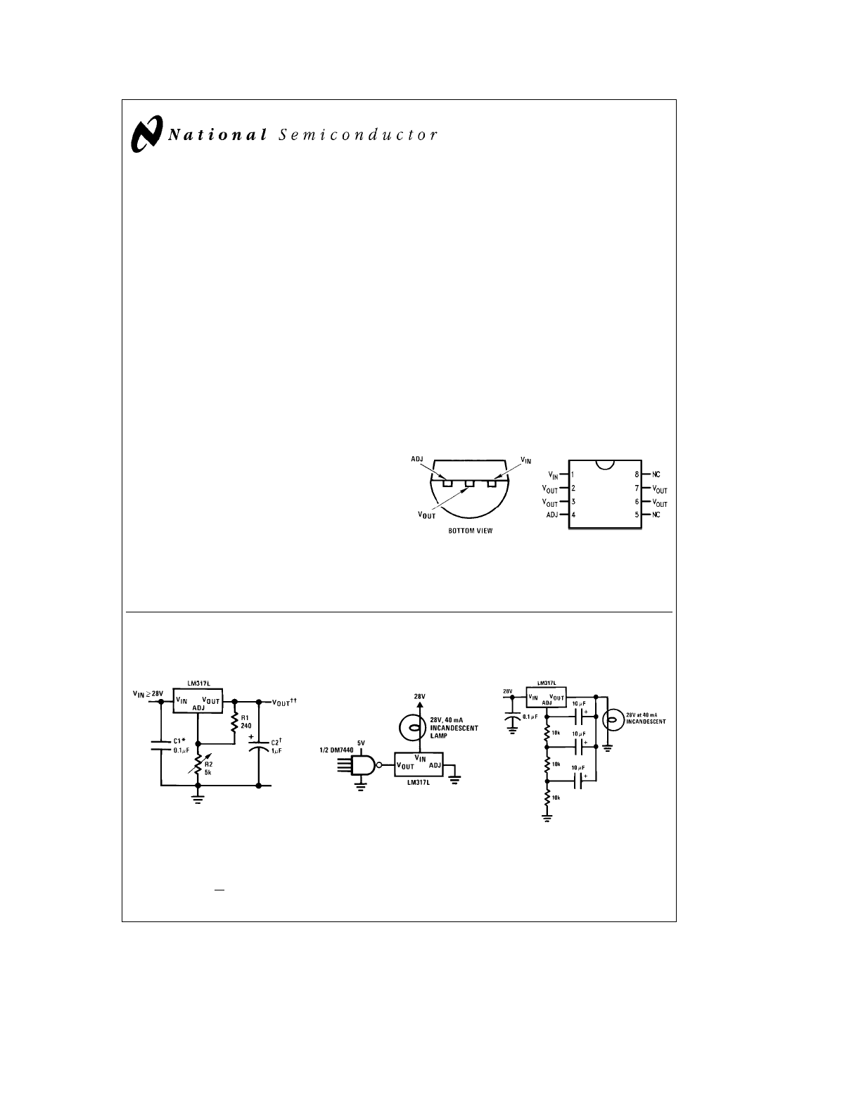
Connection Diagram
TL/H/9064 – 5
TL/H/9064 – 4
Order Number LM317LZ
Order Number LM317LM
See NS Package
See NS Package
Number Z03A
Number M08A
Typical Applications
1.2V – 25V Adjustable Regulator
TL/H/9064 – 1
Full output current not available at high input-out-
put voltages
²OptionalÐimproves transient response
*Needed if device is more than 6 inches from
filter capacitors
²²V
OUT
e
1.25V
#
1 a
R2
R1
J
a
I
ADJ
(R
2
)
Fully Protected (Bulletproof)
Lamp Driver
TL/H/9064 – 2
Lamp Flasher
TL/H/9064 – 3
Output rateÐ4 flashes per second at 10% duty
cycle
C1995 National Semiconductor Corporation
RRD-B30M115/Printed in U. S. A.
Absolute Maximum Ratings
If Military/Aerospace specified devices are required,
please contact the National Semiconductor Sales
Office/Distributors for availability and specifications.
Power Dissipation
Internally Limited
Input-Output Voltage Differential
40V
Operating Junction Temperature Range
b
40
§
C to
a
125
§
C
Storage Temperature
b
55
§
C to
a
150
§
C
Lead Temperature (Soldering, 4 seconds)
260
§
C
Output is Short Circuit Protected
ESD rating to be determined.
Electrical Characteristics
(Note 1)
Parameter
Conditions
Min
Typ
Max
Units
Line Regulation
T
j
e
25
§
C, 3V
s
(V
IN
b
V
OUT
)
s
40V, I
L
s
20 mA (Note 2)
0.01
0.04
%/V
Load Regulation
T
j
e
25
§
C, 5 mA
s
I
OUT
s
I
MAX
, (Note 2)
0.1
0.5
%
Thermal Regulation
T
j
e
25
§
C, 10 ms Pulse
0.04
0.2
%/W
Adjustment Pin Current
50
100
m
A
Adjustment Pin Current Change
5 mA
s
I
L
s
100 mA
0.2
5
m
A
3V
s
(V
IN
b
V
OUT
)
s
40V, P
s
625 mW
Reference Voltage
3V
s
(V
IN
b
V
OUT
)
s
40V, (Note 3)
1.20
1.25
1.30
V
5 mA
s
I
OUT
s
100 mA, P
s
625 mW
Line Regulation
3V
s
(V
IN
b
V
OUT
)
s
40V, I
L
s
20 mA (Note 2)
0.02
0.07
%/V
Load Regulation
5 mA
s
I
OUT
s
100 mA, (Note 2)
0.3
1.5
%
Temperature Stability
T
MIN
s
T
j
s
T
Max
0.65
%
Minimum Load Current
(V
IN
b
V
OUT
)
s
40V
3.5
5
mA
3V
s
(V
IN
b
V
OUT
)
s
15V
1.5
2.5
Current Limit
3V
s
(V
IN
b
V
OUT
)
s
13V
100
200
300
mA
(V
IN
b
V
OUT
)
e
40V
25
50
150
mA
Rms Output Noise, % of V
OUT
T
j
e
25
§
C, 10 Hz
s
f
s
10 kHz
0.003
%
Ripple Rejection Ratio
V
OUT
e
10V, f
e
120 Hz, C
ADJ
e
0
65
dB
C
ADJ
e
10 mF
66
80
dB
Long-Term Stability
T
j
e
125
§
C, 1000 Hours
0.3
1
%
Thermal Resistance
Z Package 0.4
×
Leads
180
§
C/W
Junction to Ambient
Z Package 0.125 Leads
160
§
C/W
SO-8 Package
165
§
C/W
Thermal Rating of SO Package
165
§
C/W
Note 1:
Unless otherwise noted, these specifications apply: b25
§
C
s
T
j
s
125
§
C for the LM317L; V
IN
b
V
OUT
e
5V and I
OUT
e
40 mA. Although power
dissipation is internally limited, these specifications are applicable for power dissipations up to 625 mW. I
MAX
is 100 mA.
Note 2:
Regulation is measured at constant junction temperature, using pulse testing with a low duty cycle. Changes in output voltage due to heating effects are
covered under the specification for thermal regulation.
Note 3:
Thermal resistance of the TO-92 package is 180
§
C/W junction to ambient with 0.4
×
leads from a PC board and 160
§
C/W junction to ambient with 0.125
×
lead length to PC board.
2
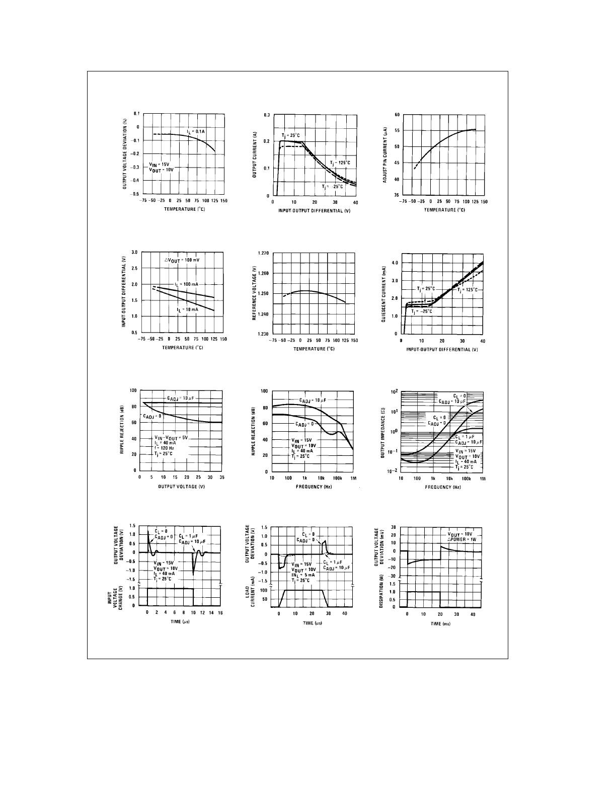
Typical Performance Characteristics
(Output capacitor
e
0 mF unless otherwise noted.)
Load Regulation
Current Limit
Adjustment Current
Dropout Voltage
Temperature Stability
Reference Voltage
Minimum Operating Current
Ripple Rejection
Ripple Rejection
Output Impedance
Line Transient Response
Load Transient Response
Thermal Regulation
TL/H/9064 – 6
3
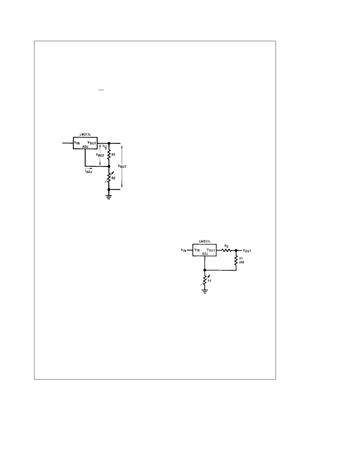
Application Hints
In operation, the LM317L develops a nominal 1.25V refer-
ence voltage, V
REF
, between the output and adjustment ter-
minal. The reference voltage is impressed across program
resistor R1 and, since the voltage is constant, a constant
current I
1
then flows through the output set resistor R2, giv-
ing an output voltage of
V
OUT
e
V
REF
#
1
a
R2
R1
J
a
I
ADJ
(R2)
Since the 100 mA current from the adjustment terminal rep-
resents an error term, the LM317L was designed to mini-
mize I
ADJ
and make it very constant with line and load
changes. To do this, all quiescent operating current is re-
turned to the output establishing a minimum load current
requirement. If there is insufficient load on the output, the
output will rise.
TL/H/9064 – 7
FIGURE 1
External Capacitors
An input bypass capacitor is recommended in case the reg-
ulator is more than 6 inches away from the usual large filter
capacitor. A 0.1 mF disc or 1 mF solid tantalum on the input
is suitable input bypassing for almost all applications. The
device is more sensitive to the absence of input bypassing
when adjustment or output capacitors are used, but the
above values will eliminate the possiblity of problems.
The adjustment terminal can be bypassed to ground on the
LM317L to improve ripple rejection and noise. This bypass
capacitor prevents ripple and noise from being amplified as
the output voltage is increased. With a 10 mF bypass capac-
itor 80 dB ripple rejection is obtainable at any output level.
Increases over 10 mF do not appreciably improve the ripple
rejection at frequencies above 120 Hz. If the bypass capaci-
tor is used, it is sometimes necessary to include protection
diodes to prevent the capacitor from discharging through
internal low current paths and damaging the device.
In general, the best type of capacitors to use is solid tanta-
lum.
Solid tantalum capacitors have low impedance even at
high frequencies.
Depending upon capacitor construction, it
takes about 25 mF in aluminum electrolytic to equal 1 mF
solid tantalum at high frequencies. Ceramic capacitors are
also good at high frequencies; but some types have a large
decrease in capacitance at frequencies around 0.5 MHz.
For this reason, a 0.01 mF disc may seem to work better
than a 0.1 mF disc as a bypass.
Although the LM317L is stable with no output capacitors,
like any feedback circuit, certain values of external capaci-
tance can cause excessive ringing. This occurs with values
between 500 pF and 5000 pF. A 1 mF solid tantalum (or 25
m
F aluminum electrolytic) on the output swamps this effect
and insures stability.
Load Regulation
The LM317L is capable of providing extremely good load
regulation but a few precautions are needed to obtain maxi-
mum performance. The current set resistor connected be-
tween the adjustment terminal and the output terminal (usu-
ally 240X) should be tied directly to the output of the regula-
tor rather than near the load. This eliminates line drops from
appearing effectively in series with the reference and de-
grading regulation. For example, a 15V regulator with 0.05X
resistance between the regulator and load will have a load
regulation due to line resistance of 0.05X
c
I
L
. If the set
resistor is connected near the load the effective line resist-
ance will be 0.05X (1
a
R2/R1) or in this case, 11.5 times
worse.
Figure 2
shows the effect of resistance between the regula-
tor and 240X set resistor.
With the TO-92 package, it is easy to minimize the resist-
ance from the case to the set resistor, by using two sepa-
rate leads to the output pin. The ground of R2 can be re-
turned near the ground of the load to provide remote ground
sensing and improve load regulation.
TL/H/9064 – 8
FIGURE 2. Regulator with Line Resistance
in Output Lead
4
Application Hints
(Continued)
Thermal Regulation
When power is dissipated in an IC, a temperature gradient
occurs across the IC chip affecting the individual IC circuit
components. With an IC regulator, this gradient can be es-
pecially severe since power dissipation is large. Thermal
regulation is the effect of these temperature gradients on
output voltage (in percentage output change) per watt of
power change in a specified time. Thermal regulation error
is independent of electrical regulation or temperature coeffi-
cient, and occurs within 5 ms to 50 ms after a change in
power dissipation. Thermal regulation depends on IC layout
as well as electrical design. The thermal regulation of a volt-
age regulator is defined as the percentage change of V
OUT
,
per watt, within the first 10 ms after a step of power is ap-
plied. The LM317L specification is 0.2%/W, maximum.
In the Thermal Regulation curve at the bottom of the Typical
Performance Characteristics page, a typical LM317L’s out-
put changes only 7 mV (or 0.07% of V
OUT
e b
10V) when
a 1W pulse is applied for 10 ms. This performance is thus
well inside the specification limit of 0.2%/W
c
1W
e
0.2%
maximum. When the 1W pulse is ended, the thermal regula-
tion again shows a 7 mV change as the gradients across the
LM317L chip die out. Note that the load regulation error of
about 14 mV (0.14%) is additional to the thermal regulation
error.
Protection Diodes
When external capacitors are used with
any
IC regulator it is
sometimes necessary to add protection diodes to pre-
vent the capacitors from discharging through low current
points into the regulator. Most 10 mF capacitors have low
enough internal series resistance to deliver 20A spikes
when shorted. Although the surge is short, there is enough
energy to damage parts of the IC.
When an output capacitor is connected to a regulator and
the input is shorted, the output capacitor will discharge into
the output of the regulator. The discharge current depends
on the value of the capacitor, the output voltage of the regu-
lator, and the rate of decrease of V
IN
. In the LM317L, this
discharge path is through a large junction that is able to
sustain a 2A surge with no problem. This is not true of other
types of positive regulators. For output capacitors of 25 mF
or less, the LM317L’s ballast resistors and output structure
limit the peak current to a low enough level so that there is
no need to use a protection diode.
The bypass capacitor on the adjustment terminal can dis-
charge through a low current junction. Discharge occurs
when
either
the input or output is shorted. Internal to the
LM317L is a 50X resistor which limits the peak discharge
current. No protection is needed for output voltages of 25V
or less and 10 mF capacitance.
Figure 3
shows an LM317L
with protection diodes included for use with outputs greater
than 25V and high values of output capacitance.
TL/H/9064 – 9
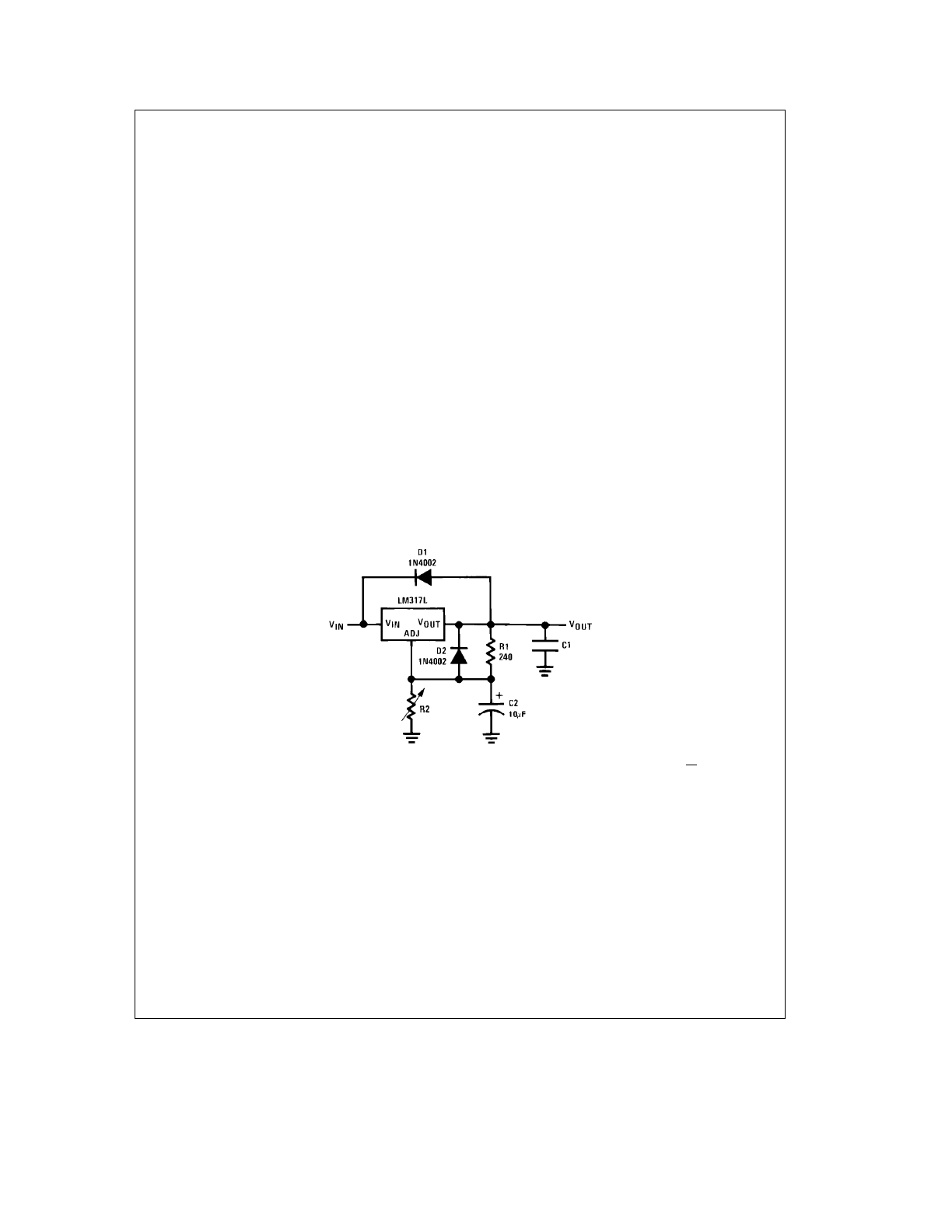
FIGURE 3. Regulator with Protection Diodes
V
OUT
e
1.25V
#
1 a
R2
R1
J
I
ADJ
R2
D1 protects against C1
D2 protects against C2
5
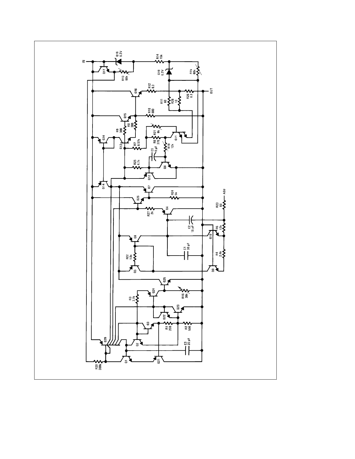
Schematic Diagram
TL/H/9064
–
1
0
6
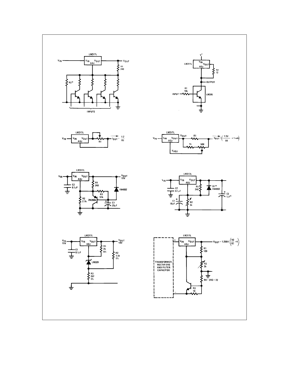
Typical Applications
(Continued)
Digitally Selected Outputs
TL/H/9064 – 11
*Sets maximum V
OUT
High Gain Amplifier
TL/H/9064 – 12
Adjustable Current Limiter
TL/H/9064 – 13
12
s
R1
s
240
Precision Current Limiter
TL/H/9064 – 14
Slow Turn-On 15V Regulator
TL/H/9064 – 15
Adjustable Regulator with
Improved Ripple Rejection
²Solid tantalum
TL/H/9064 – 16
*Discharges C1 if output is shorted to ground
High Stability 10V Regulator
TL/H/9064 – 17
Adjustable Regulator with Current Limiter
TL/H/9064 – 18
Short circuit current is approximately 600 mV/R3, or 60 mA (compared to
LM317LZ’s 200 mA current limit).
At 25 mA output only 3/4V of drop occurs in R3 and R4.
7
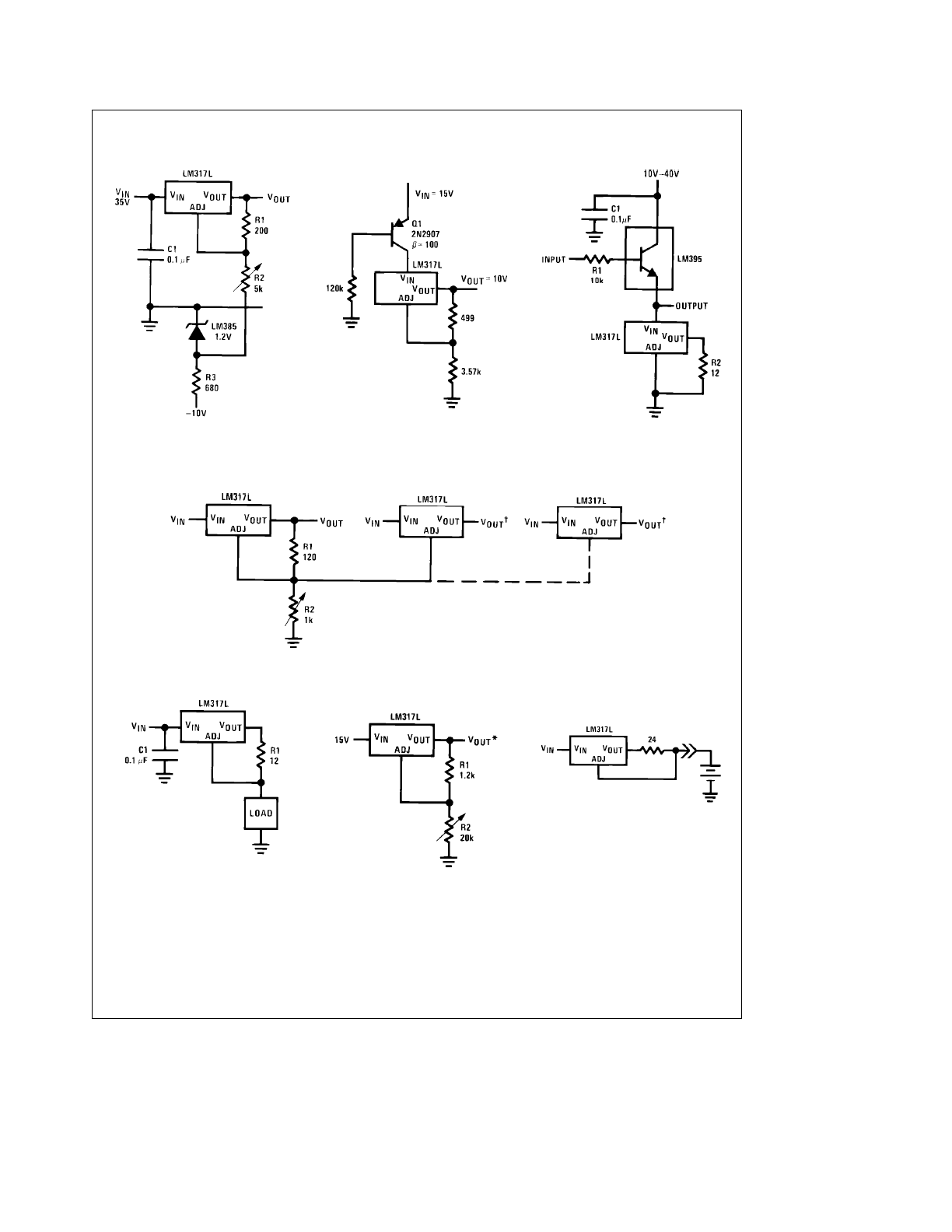
Typical Applications
(Continued)
0V – 30V Regulator
TL/H/9064 – 19
Full output current not available at high input-out-
put voltages
Regulator With 15 mA Short Circuit
Current
TL/H/9064 – 20
Power Follower
TL/H/9064 – 21
Adjusting Multiple On-Card Regulators with Single Control
*
*All outputs within
g
100 mV
²Minimum load b5mA
TL/H/9064 – 22
100 mA Current Regulator
TL/H/9064 – 23
1.2V – 12V Regulator with Minimum
Program Current
*Minimum load current & 2 mA
TL/H/9064 – 24
50 mA Constant Current Battery
Charger for Nickel-Cadmium
Batteries
TL/H/9064 – 25
8
Typical Applications
(Continued)
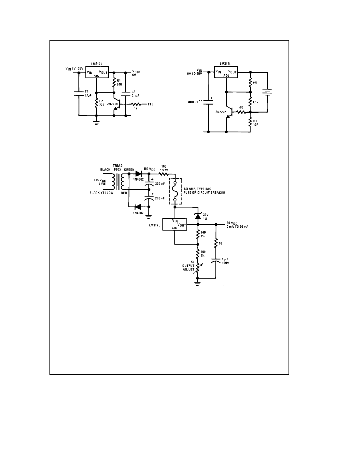
5V Logic Regulator with Electronic Shutdown
*
TL/H/9064 – 26
*Minimum output & 1.2V
Current Limited 6V Charger
TL/H/9064 – 27
*Sets peak current, I
PEAK
e
0.6V/R1
**1000 mF is recommended to filter out any input transients.
Short Circuit Protected 80V Supply
TL/H/9064 – 28
9
Typical Applications
(Continued)
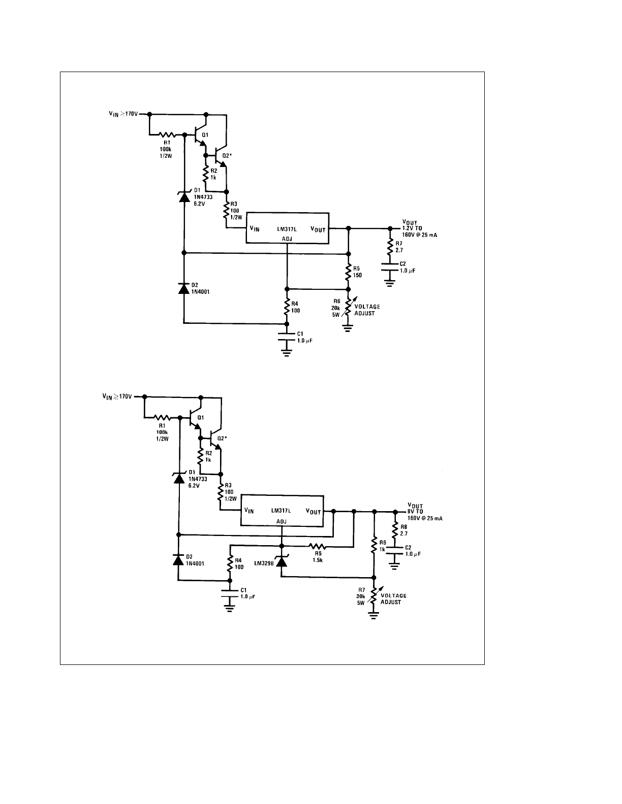
Basic High Voltage Regulator
Q1, Q2: NSD134 or similar
C1, C2: 1 mF, 200V mylar**
*Heat sink
TL/H/9064 – 29
Precision High Voltage Regulator
Q1, Q2: NSD134 or similar
C1, C2: 1 mF, 200V mylar**
*Heat sink
**Mylar is a registered trademark of DuPont Co.
TL/H/9064 – 30
10
Typical Applications
(Continued)
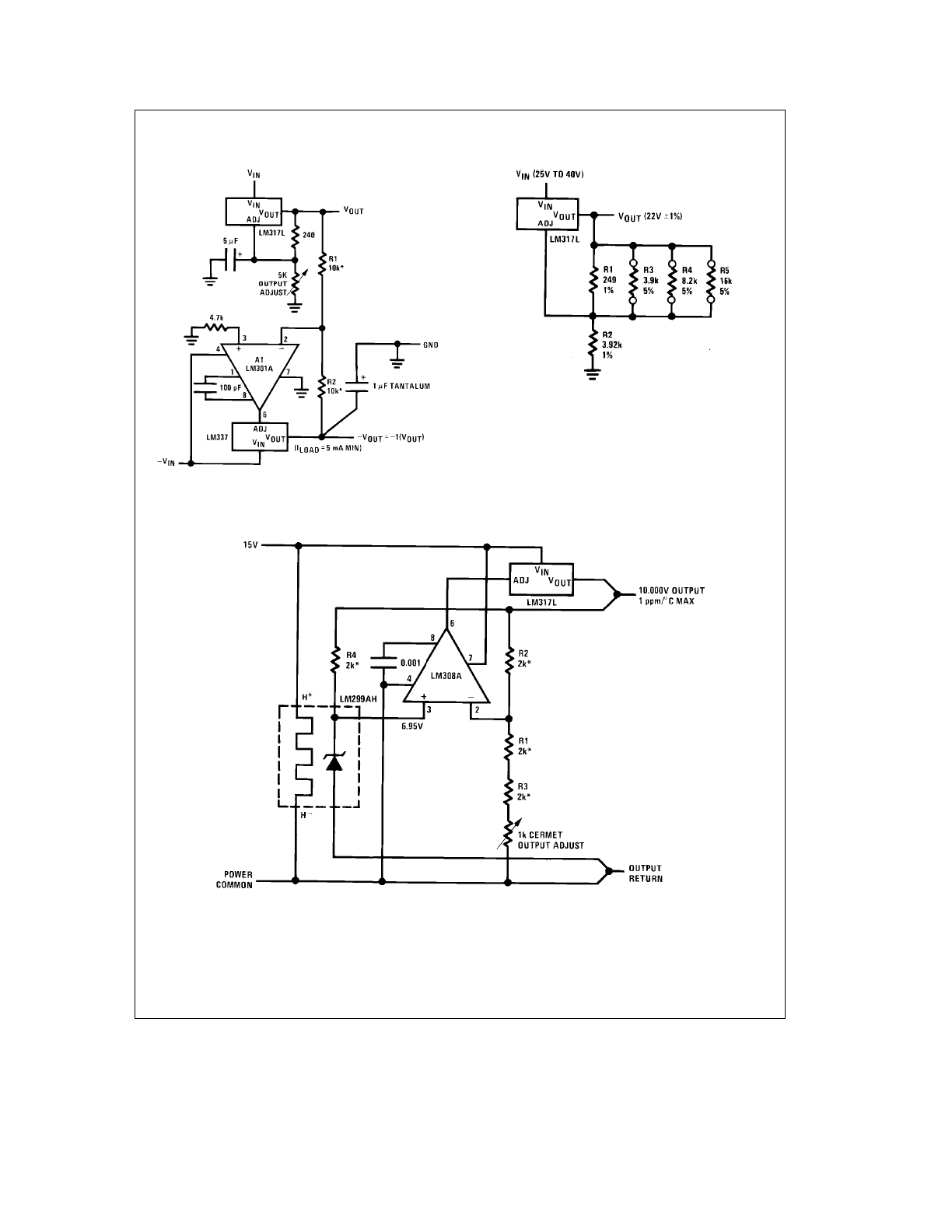
Tracking Regulator
TL/H/9064 – 31
A1 e LM301A, LM307, or LF13741 only
R1, R2 e matched resistors with good TC tracking
Regulator With Trimmable Output Voltage
TL/H/9064 – 32
Trim Procedure:
Ð If V
OUT
is 23.08V or higher, cut out R3 (if lower, don’t cut it out).
Ð Then if V
OUT
is 22.47V or higher, cut out R4 (if lower, don’t).
Ð Then if V
OUT
is 22.16V or higher, cut out R5 (if lower, don’t).
This will trim the output to well within
g
1% of 22.00 V
DC
, without any of the
expense or uncertainty of a trim pot (see LB-46). Of course, this technique
can be used at any output voltage level.
Precision Reference with Short-Circuit Proof Output
TL/H/9064 – 33
*R1–R4 from thin-film network,
Beckman 694-3-R2K-D or similar
11

12
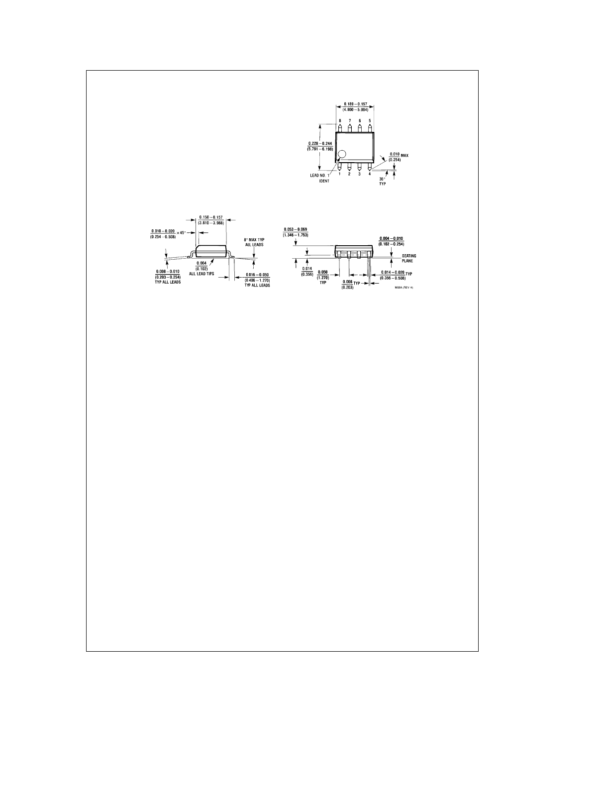
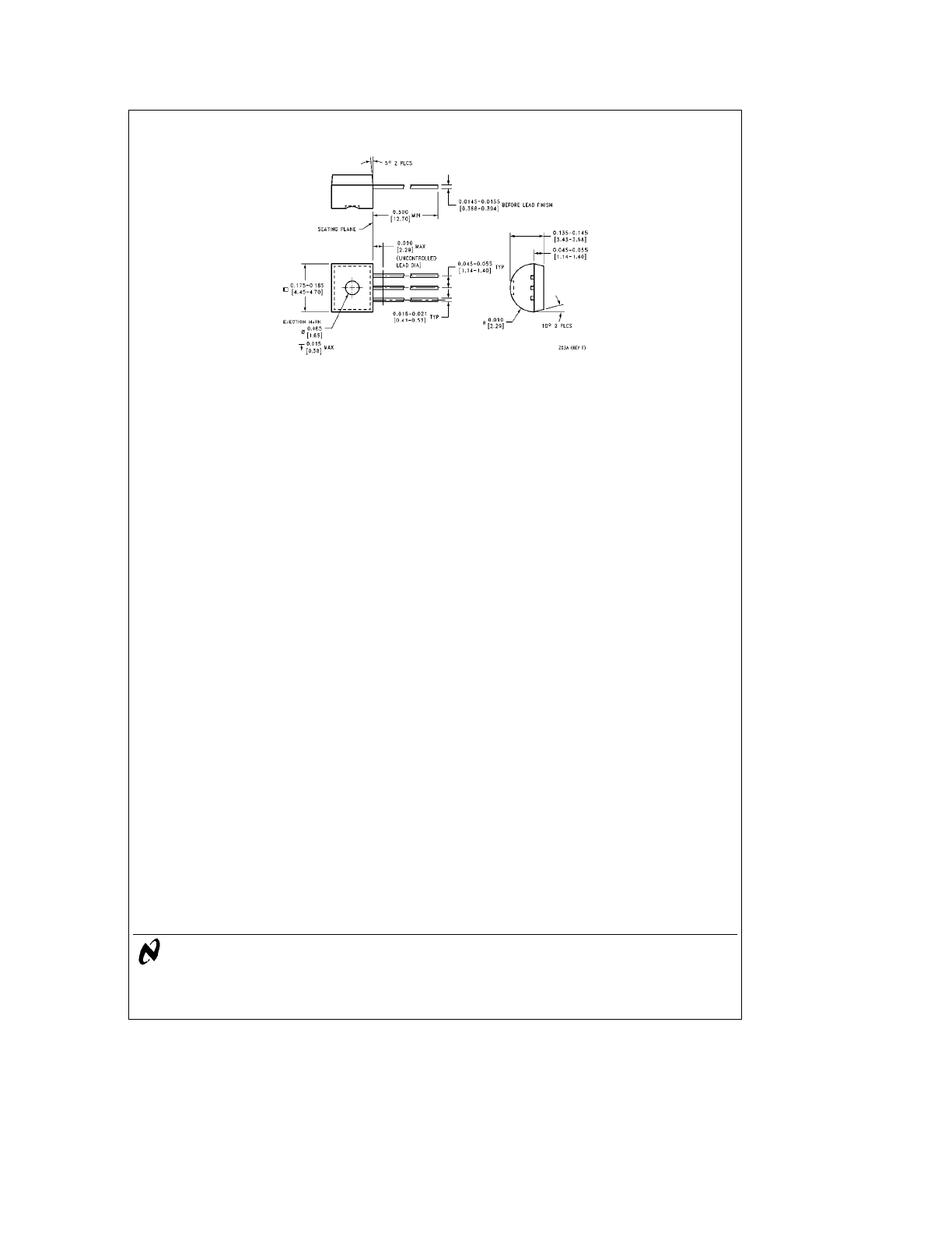
Physical Dimensions
inches (millimeters)
SO-8 Molded Package
Order Number LM317LM
NS Package Number M08A
13
LM317L
3-Terminal
Adjustable
Regulator
Physical Dimensions
inches (millimeters) (Continued)
TO-92 Plastic Package (Z)
Order Number LM317LZ
NS Package Number Z03A
LIFE SUPPORT POLICY
NATIONAL’S PRODUCTS ARE NOT AUTHORIZED FOR USE AS CRITICAL COMPONENTS IN LIFE SUPPORT
DEVICES OR SYSTEMS WITHOUT THE EXPRESS WRITTEN APPROVAL OF THE PRESIDENT OF NATIONAL
SEMICONDUCTOR CORPORATION. As used herein:
1. Life support devices or systems are devices or
2. A critical component is any component of a life
systems which, (a) are intended for surgical implant
support device or system whose failure to perform can
into the body, or (b) support or sustain life, and whose
be reasonably expected to cause the failure of the life
failure to perform, when properly used in accordance
support device or system, or to affect its safety or
with instructions for use provided in the labeling, can
effectiveness.
be reasonably expected to result in a significant injury
to the user.
National Semiconductor
National Semiconductor
National Semiconductor
National Semiconductor
Corporation
Europe
Hong Kong Ltd.
Japan Ltd.
1111 West Bardin Road
Fax: (
a
49) 0-180-530 85 86
13th Floor, Straight Block,
Tel: 81-043-299-2309
Arlington, TX 76017
Email: cnjwge
@
tevm2.nsc.com
Ocean Centre, 5 Canton Rd.
Fax: 81-043-299-2408
Tel: 1(800) 272-9959
Deutsch Tel: (
a
49) 0-180-530 85 85
Tsimshatsui, Kowloon
Fax: 1(800) 737-7018
English
Tel: (
a
49) 0-180-532 78 32
Hong Kong
Fran
3ais Tel: (
a
49) 0-180-532 93 58
Tel: (852) 2737-1600
Italiano
Tel: (
a
49) 0-180-534 16 80
Fax: (852) 2736-9960
National does not assume any responsibility for use of any circuitry described, no circuit patent licenses are implied and National reserves the right at any time without notice to change said circuitry and specifications.