
LM2598
SIMPLE SWITCHER
®
Power Converter 150 kHz
1A Step-Down Voltage Regulator, with Features
General Description
The LM2598 series of regulators are monolithic integrated
circuits that provide all the active functions for a step-down
(buck) switching regulator, capable of driving a 1A load with
excellent line and load regulation. These devices are avail-
able in fixed output voltages of 3.3V, 5V, 12V, and an adjust-
able output version.
This series of switching regulators is similar to the LM2595
series, with additional supervisory and performance features
added.
Requiring a minimum number of external components, these
regulators are simple to use and include internal frequency
compensation
†
, improved line and load specifications,
fixed-frequency oscillator, Shutdown /Soft-start, error flag
delay and error flag output.
The LM2598 series operates at a switching frequency of 150
kHz thus allowing smaller sized filter components than what
would be needed with lower frequency switching regulators.
Available in a standard 7-lead TO-220 package with several
different lead bend options, and a 7-lead TO-263 surface
mount package. Typically, for output voltages less than 12V,
and ambient temperatures less than 50˚C, no heat sink is re-
quired.
A standard series of inductors (both through hole and sur-
face mount types) are available from several different manu-
facturers optimized for use with the LM2598 series. This fea-
ture greatly simplifies the design of switch-mode power
supplies.
Other features include a guaranteed
±
4% tolerance on out-
put voltage under all conditions of input voltage and output
load conditions, and
±
15% on the oscillator frequency. Ex-
ternal shutdown is included, featuring typically 85 µA
standby current. Self protection features include a two stage
current limit for the output switch and an over temperature
shutdown for complete protection under fault conditions.
Features
n
3.3V, 5V, 12V, and adjustable output versions
n
Adjustable version output voltage range, 1.2V to 37V
±
4% max over line and load conditions
n
Guaranteed 1A output current
n
Available in 7-pin TO-220 and TO-263 (surface mount)
package
n
Input voltage range up to 40V
n
Excellent line and load regulation specifications
n
150 kHz fixed frequency internal oscillator
n
Shutdown /Soft-start
n
Out of regulation error flag
n
Error output delay
n
Low power standby mode, I
Q
typically 85 µA
n
High Efficiency
n
Uses readily available standard inductors
n
Thermal shutdown and current limit protection
Applications
n
Simple high-efficiency step-down (buck) regulator
n
Efficient pre-regulator for linear regulators
n
On-card switching regulators
n
Positive to Negative converter
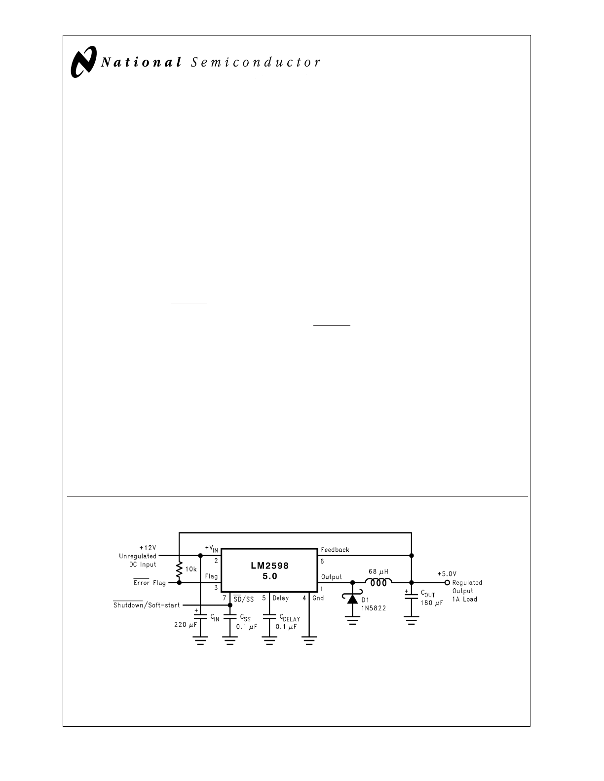
Typical Application
(Fixed Output Voltage Versions)
†
Patent Number 5,382,918.
SIMPLE SWITCHER
®
and
Switchers Made Simple
®
are registered trademarks of National Semiconductor Corporation.
DS012593-1
March 1998
LM2598
SIMPLE
SWITCHER
Power
Converter
150
kHz
1A
Step-Down
V
oltage
Regulator
,
with
Features
© 2000 National Semiconductor Corporation
DS012593
www.national.com
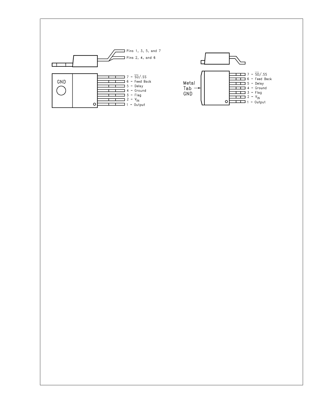
Connection Diagrams and Order Information
Bent and Staggered Leads, Through Hole Package
7-Lead TO-220 (T)
DS012593-50
Order Number LM2598T-3.3, LM2598T-5.0,
LM2598T-12 or LM2598T-ADJ
See NS Package Number TA07B
Surface Mount Package
7-Lead TO-263 (S)
DS012593-22
Order Number LM2598S-3.3, LM2598S-5.0,
LM2598S-12 or LM2598S-ADJ
See NS Package Number TS7B
LM2598
www.national.com
2
Absolute Maximum Ratings
(Note 1)
If Military/Aerospace specified devices are required,
please contact the National Semiconductor Sales Office/
Distributors for availability and specifications.
Maximum Supply Voltage (V
IN
)
45V
SD/SS Pin Input Voltage (Note 2)
6V
Delay Pin Voltage (Note 2)
1.5V
Flag Pin Voltage
−0.3
≤
V
≤
+45V
Feedback Pin Voltage
−0.3
≤
V
≤
+25V
Output Voltage to Ground
(Steady State)
−1V
Power Dissipation
Internally limited
Storage Temperature Range
−65˚C to +150˚C
ESD Susceptibility
Human Body Model (Note 3)
2 kV
Lead Temperature
S Package
Vapor Phase (60 sec.)
+215˚C
Infrared (10 sec.)
+245˚C
T Package (Soldering, 10 sec.)
+260˚C
Maximum Junction Temperature
+150˚C
Operating Conditions
Temperature Range
−25˚C
≤
T
J
≤
+125˚C
Supply Voltage
4.5V to 40V
LM2598-3.3
Electrical Characteristics
Specifications with standard type face are for T
J
= 25˚C, and those with boldface type apply over full Operating Tempera-
ture Range.
Symbol
Parameter
Conditions
LM2598-3.3
Units
(Limits)
Typ
Limit
(Note 4)
(Note 5)
SYSTEM PARAMETERS (Note 6) Test Circuit
Figure 1
V
OUT
Output Voltage
4.75V
≤
V
IN
≤
40V, 0.1A
≤
I
LOAD
≤
1A
3.3
V
3.168/3.135
V(min)
3.432/3.465
V(max)
η
Efficiency
V
IN
= 12V, I
LOAD
= 1A
78
%
LM2598-5.0
Electrical Characteristics
Specifications with standard type face are for T
J
= 25˚C, and those with boldface type apply over full Operating Tempera-
ture Range.
Symbol
Parameter
Conditions
LM2598-5.0
Units
(Limits)
Typ
Limit
(Note 4)
(Note 5)
SYSTEM PARAMETERS (Note 6) Test Circuit
Figure 1
V
OUT
Output Voltage
7V
≤
V
IN
≤
40V, 0.1A
≤
I
LOAD
≤
1A
5
V
4.800/4.750
V(min)
5.200/5.250
V(max)
η
Efficiency
V
IN
= 12V, I
LOAD
= 1A
82
%
LM2598-12
Electrical Characteristics
Specifications with standard type face are for T
J
= 25˚C, and those with boldface type apply over full Operating Tempera-
ture Range.
Symbol
Parameter
Conditions
LM2598-12
Units
(Limits)
Typ
Limit
(Note 4)
(Note 5)
SYSTEM PARAMETERS (Note 6) Test Circuit
Figure 1
V
OUT
Output Voltage
15V
≤
V
IN
≤
40V, 0.1A
≤
I
LOAD
≤
1A
12
V
11.52/11.40
V(min)
12.48/12.60
V(max)
η
Efficiency
V
IN
= 25V, I
LOAD
= 1A
90
%
LM2598
www.national.com
3
LM2598-ADJ
Electrical Characteristics
Specifications with standard type face are for T
J
= 25˚C, and those with boldface type apply over full Operating Tempera-
ture Range.
Symbol
Parameter
Conditions
LM2598-ADJ
Units
(Limits)
Typ
Limit
(Note 4)
(Note 5)
SYSTEM PARAMETERS (Note 6) Test Circuit
Figure 1
V
FB
Feedback Voltage
4.5V
≤
V
IN
≤
40V, 0.1A
≤
I
LOAD
≤
1A
1.230
V
V
OUT
programmed for 3V. Circuit of
Figure 12
.
1.193/1.180
V(min)
1.267/1.280
V(max)
η
Efficiency
V
IN
= 12V, V
OUT
= 3V, I
LOAD
= 1A
78
%
All Output Voltage Versions
Electrical Characteristics
Specifications with standard type face are for T
J
= 25˚C, and those with boldface type apply over full Operating Temperature
Range. Unless otherwise specified, V
IN
= 12V for the 3.3V, 5V, and Adjustable version and V
IN
= 24V for the 12V version.
I
LOAD
= 200 mA
Symbol
Parameter
Conditions
LM2598-XX
Units
(Limits)
Typ
Limit
(Note 4)
(Note 5)
DEVICE PARAMETERS
I
b
Feedback Bias Current
Adjustable Version Only, V
FB
= 1.3V
10
nA
50/100
nA(max)
f
O
Oscillator Frequency
(Note 7)
150
kHz
127/110
kHz(min)
173/173
kHz(max)
V
SAT
Saturation Voltage
I
OUT
= 1A (Note 8) (Note 9)
1
V
1.2/1.3
V(max)
DC
Max Duty Cycle (ON)
(Note 9)
100
%
Min Duty Cycle (OFF)
(Note 10)
0
I
CL
Current Limit
Peak Current, (Note 8) (Note 9)
1.5
A
1.2/1.15
A(min)
2.4/2.6
A(max)
I
L
Output Leakage Current
Output = 0V (Note 9) (Note 10) (Note 11)
50
µA(max)
Output = −1V
2
mA
15
mA(max)
I
Q
Operating Quiescent
SD /SS Pin Open, (Note 10)
5
mA
Current
10
mA(max)
I
STBY
Standby Quiescent
SD /SS pin = 0V, (Note 11)
85
µA
Current
200/250
µA(max)
θ
JC
Thermal Resistance
TO220 or TO263 Package, Junction to Case
2
˚C/W
θ
JA
TO220 Package, Junction to Ambient (Note 12)
50
˚C/W
θ
JA
TO263 Package, Junction to Ambient (Note 13)
50
˚C/W
θ
JA
TO263 Package, Junction to Ambient (Note 14)
30
˚C/W
θ
JA
TO263 Package, Junction to Ambient (Note 15)
20
˚C/W
SHUTDOWN/SOFT-START CONTROL Test Circuit of
Figure 1
V
SD
Shutdown Threshold
1.3
V
Voltage
Low, (Shutdown Mode)
0.6
V(max)
High, (Soft-start Mode)
2
V(min)
V
SS
Soft-start Voltage
V
OUT
= 20% of Nominal Output Voltage
2
V
V
OUT
= 100% of Nominal Output Voltage
3
LM2598
www.national.com
4
All Output Voltage Versions
Electrical Characteristics
(Continued)
Specifications with standard type face are for T
J
= 25˚C, and those with boldface type apply over full Operating Temperature
Range. Unless otherwise specified, V
IN
= 12V for the 3.3V, 5V, and Adjustable version and V
IN
= 24V for the 12V version.
I
LOAD
= 200 mA
Symbol
Parameter
Conditions
LM2598-XX
Units
(Limits)
Typ
Limit
(Note 4)
(Note 5)
SHUTDOWN/SOFT-START CONTROL Test Circuit of
Figure 1
I
SD
Shutdown Current
V
SHUTDOWN
= 0.5V
5
µA
10
µA(max)
I
SS
Soft-start Current
V
Soft-start
= 2.5V
1.6
µA
5
µA(max)
FLAG/DELAY CONTROL Test Circuit of
Figure 1
Regulator Dropout Detector
Low (Flag ON)
96
%
Threshold Voltage
92
%(min)
98
%(max)
VF
SAT
Flag Output Saturation
I
SINK
= 3 mA
0.3
V
Voltage
V
DELAY
= 0.5V
0.7/1.0
V(max)
IF
L
Flag Output Leakage
Current
V
FLAG
= 40V
0.3
µA
Delay Pin Threshold
1.25
V
Voltage
Low (Flag ON)
1.21
V(min)
High (Flag OFF) and V
OUT
Regulated
1.29
V(max)
Delay Pin Source Current
V
DELAY
= 0.5V
3
µA
6
µA(max)
Delay Pin Saturation
Low (Flag ON)
55
mV
350/400
mV(max)
Note 1: Absolute Maximum Ratings indicate limits beyond which damage to the device may occur. Operating Ratings indicate conditions for which the device is in-
tended to be functional, but do not guarantee specific performance limits. For guaranteed specifications and test conditions, see the Electrical Characteristics.
Note 2: Voltage internally clamped. If clamp voltage is exceeded, limit current to a maximum of 1 mA.
Note 3: The human body model is a 100 pF capacitor discharged through a 1.5k resistor into each pin.
Note 4: Typical numbers are at 25˚C and represent the most likely norm.
Note 5: All limits guaranteed at room temperature (standard type face) and at temperature extremes (bold type face). All room temperature limits are 100% pro-
duction tested. All limits at temperature extremes are guaranteed via correlation using standard Statistical Quality Control (SQC) methods. All limits are used to cal-
culate Average Outgoing Quality Level (AOQL).
Note 6: External components such as the catch diode, inductor, input and output capacitors can affect switching regulator system performance. When the LM2598
is used as shown in the
Figure 1 test circuit, system performance will be as shown in system parameters section of Electrical Characteristics.
Note 7: The switching frequency is reduced when the second stage current limit is activated. The amount of reduction is determined by the severity of current over-
load.
Note 8: No diode, inductor or capacitor connected to output pin.
Note 9: Feedback pin removed from output and connected to 0V to force the output transistor switch ON.
Note 10: Feedback pin removed from output and connected to 12V for the 3.3V, 5V, and the ADJ. version, and 15V for the 12V version, to force the output transistor
switch OFF.
Note 11: V
IN
= 40V.
Note 12: Junction to ambient thermal resistance (no external heat sink) for the TO-220 package mounted vertically, with the leads soldered to a printed circuit board
with (1 oz.) copper area of approximately 1 in
2
.
Note 13: Junction to ambient thermal resistance with the TO-263 package tab soldered to a single sided printed circuit board with 0.5 in
2
of (1 oz.) copper area.
Note 14: Junction to ambient thermal resistance with the TO-263 package tab soldered to a single sided printed circuit board with 2.5 in
2
of (1 oz.) copper area.
Note 15: Junction to ambient thermal resistance with the TO-263 package tab soldered to a double sided printed circuit board with 3 in
2
of (1 oz.) copper area on
the LM2598S side of the board, and approximately 16 in
2
of copper on the other side of the p-c board. See application hints in this data sheet and the thermal model
in
Switchers Made Simple
®
version 4.2 software.
LM2598
www.national.com
5
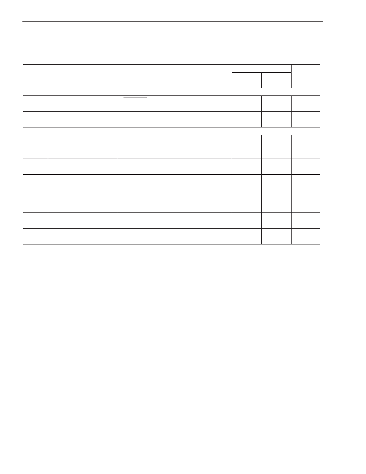
Typical Performance Characteristics
(Circuit of
Figure 1
)
Normalized
Output Voltage
DS012593-2
Line Regulation
DS012593-3
Efficiency
DS012593-14
Switch Saturation
Voltage
DS012593-15
Switch Current Limit
DS012593-16
Dropout Voltage
DS012593-17
Operating
Quiescent Current
DS012593-4
Shutdown
Quiescent Current
DS012593-5
Minimum Operating
Supply Voltage
DS012593-6
LM2598
www.national.com
6
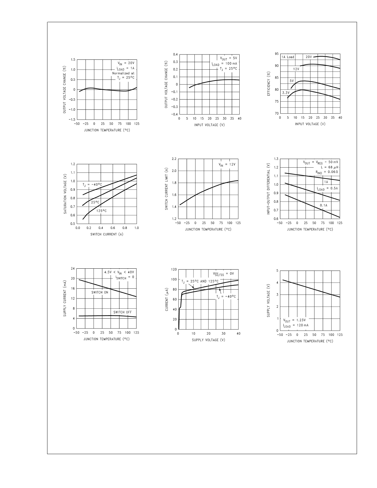
Typical Performance Characteristics
(Circuit of
Figure 1
) (Continued)
Feedback Pin
Bias Current
DS012593-49
Flag Saturation
Voltage
DS012593-7
Switching Frequency
DS012593-8
Soft-start
DS012593-9
Shutdown/Soft-start
Current
DS012593-10
Delay Pin Current
DS012593-11
Soft-start Response
DS012593-12
Shutdown/Soft-start
Threshold Voltage
DS012593-13
LM2598
www.national.com
7
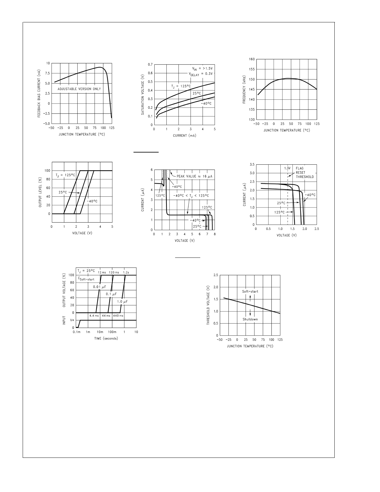
Typical Performance Characteristics
(Circuit of
Figure 1
)
Continuous Mode Switching Waveforms
V
IN
= 20V, V
OUT
= 5V, I
LOAD
= 1A
L = 68 µH, C
OUT
= 120 µF, C
OUT
ESR = 100 m
Ω
DS012593-18
A: Output Pin Voltage, 10V/div.
B: Inductor Current 0.5A/div.
C: Output Ripple Voltage, 50 mV/div.
Horizontal Time Base: 2 µs/div.
Discontinuous Mode Switching Waveforms
V
IN
= 20V, V
OUT
= 5V, I
LOAD
= 600 mA
L = 22 µH, C
OUT
= 220 µF, C
OUT
ESR = 50 m
Ω
DS012593-19
A: Output Pin Voltage, 10V/div.
B: Inductor Current 0.5A/div.
C: Output Ripple Voltage, 50 mV/div.
Horizontal Time Base: 2 µs/div.
Load Transient Response for Continuous Mode
V
IN
= 20V, V
OUT
= 5V, I
LOAD
= 250 mA to 750 mA
L = 68 µH, C
OUT
= 120 µF, C
OUT
ESR = 100 m
Ω
DS012593-20
A: Output Voltage, 100 mV/div. (AC)
B: 250 mA to 750 mA Load Pulse
Horizontal Time Base: 100 µs/div.
Load Transient Response for Discontinuous Mode
V
IN
= 20V, V
OUT
= 5V, I
LOAD
= 250 mA to 750 mA
L = 22 µH, C
OUT
= 220 µF, C
OUT
ESR = 50 m
Ω
DS012593-21
A: Output Voltage, 100 mV/div. (AC)
B: 250 mA to 750 mA Load Pulse
Horizontal Time Base: 200 µs/div.
LM2598
www.national.com
8
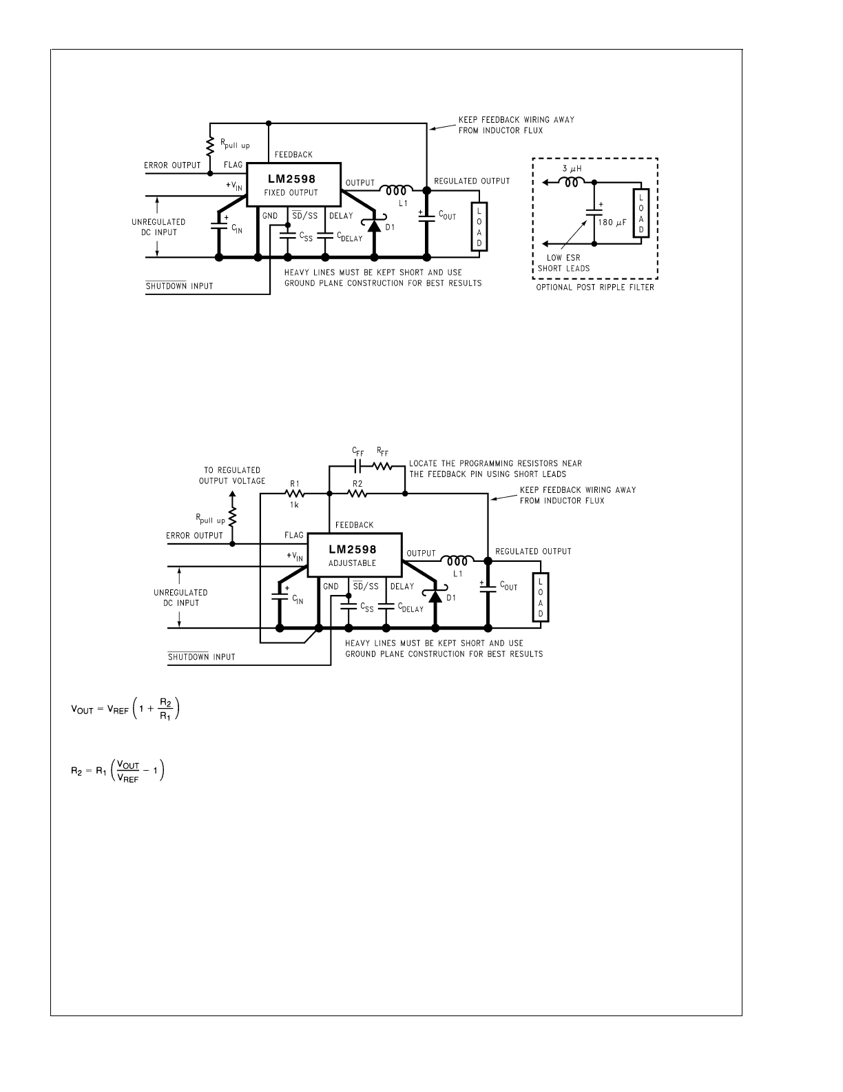
Test Circuit and Layout Guidelines
Fixed Output Voltage Versions
DS012593-23
Component Values shown are for V
IN
= 15V, V
OUT
= 5V, I
LOAD
= 1A.
120 µF, 50V, Aluminum Electrolytic Nichicon “PL Series”
120 µF, 35V Aluminum Electrolytic, Nichicon “PL Series”
3A, 40V Schottky Rectifier, 1N5822
68 µH, L30
Typical Values
*C
SS
:
— 0.1 µF
C
DELAY
:
— 0.1 µF
R
Pull Up
:
— 4.7k
Adjustable Output Voltage Versions
DS012593-24
where V
REF
= 1.23V
Select R
1
to be approximately 1k
Ω
, use a 1% resistor for best stability.
Component Values shown are for V
IN
= 20V,
V
OUT
= 10V, I
LOAD
= 1A.
C
IN
— 120 µF, 35V, Aluminum Electrolytic Nichicon “PL Series”
C
OUT
— 120 µF, 35V Aluminum Electrolytic, Nichicon “PL Series”
D1
— 3A, 40V Schottky Rectifier, 1N5822
L1
— 100 µH, L29
R
1
— 1 k
Ω
, 1%
R
2
— 7.15k, 1%
C
FF
— 3.3 nF, See Application Information Section
R
FF
— 3 k
Ω
, See Application Information Section
Typical Values
C
SS
— 0.1 µF
C
DELAY
— 0.1 µF
R
PULL UP
— 4.7k
FIGURE 1. Standard Test Circuits and Layout Guides
LM2598
www.national.com
9
Test Circuit and Layout Guidelines
(Continued)
As in any switching regulator, layout is very important. Rap-
idly switching currents associated with wiring inductance can
generate voltage transients which can cause problems. For
minimal inductance and ground loops, the wires indicated by
heavy lines should be wide printed circuit traces and
should be kept as short as possible. For best results, ex-
ternal components should be located as close to the
switcher lC as possible using ground plane construction or
single point grounding.
If open core inductors are used, special care must be
taken as to the location and positioning of this type of induc-
tor. Allowing the inductor flux to intersect sensitive feedback,
lC groundpath and C
OUT
wiring can cause problems.
When using the adjustable version, special care must be
taken as to the location of the feedback resistors and the as-
sociated wiring. Physically locate both resistors near the IC,
and route the wiring away from the inductor, especially an
open core type of inductor. (See application section for more
information.)
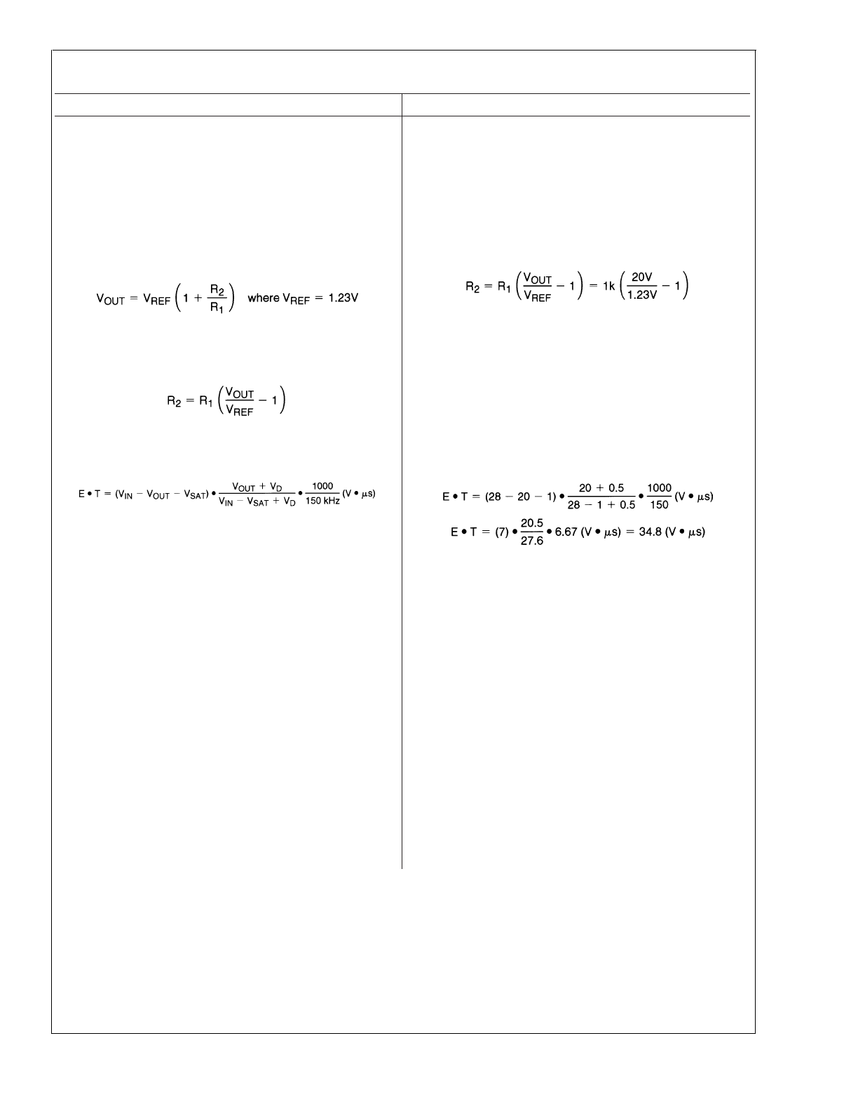
LM2598 Series Buck Regulator Design Procedure (Fixed Output)
PROCEDURE (Fixed Output Voltage Version)
EXAMPLE (Fixed Output Voltage Version)
Given:
Given:
V
OUT
= Regulated Output Voltage (3.3V, 5V or 12V)
V
OUT
= 5V
V
IN
(max) = Maximum DC Input Voltage
V
IN
(max) = 12V
I
LOAD
(max) = Maximum Load Current
I
LOAD
(max) = 1A
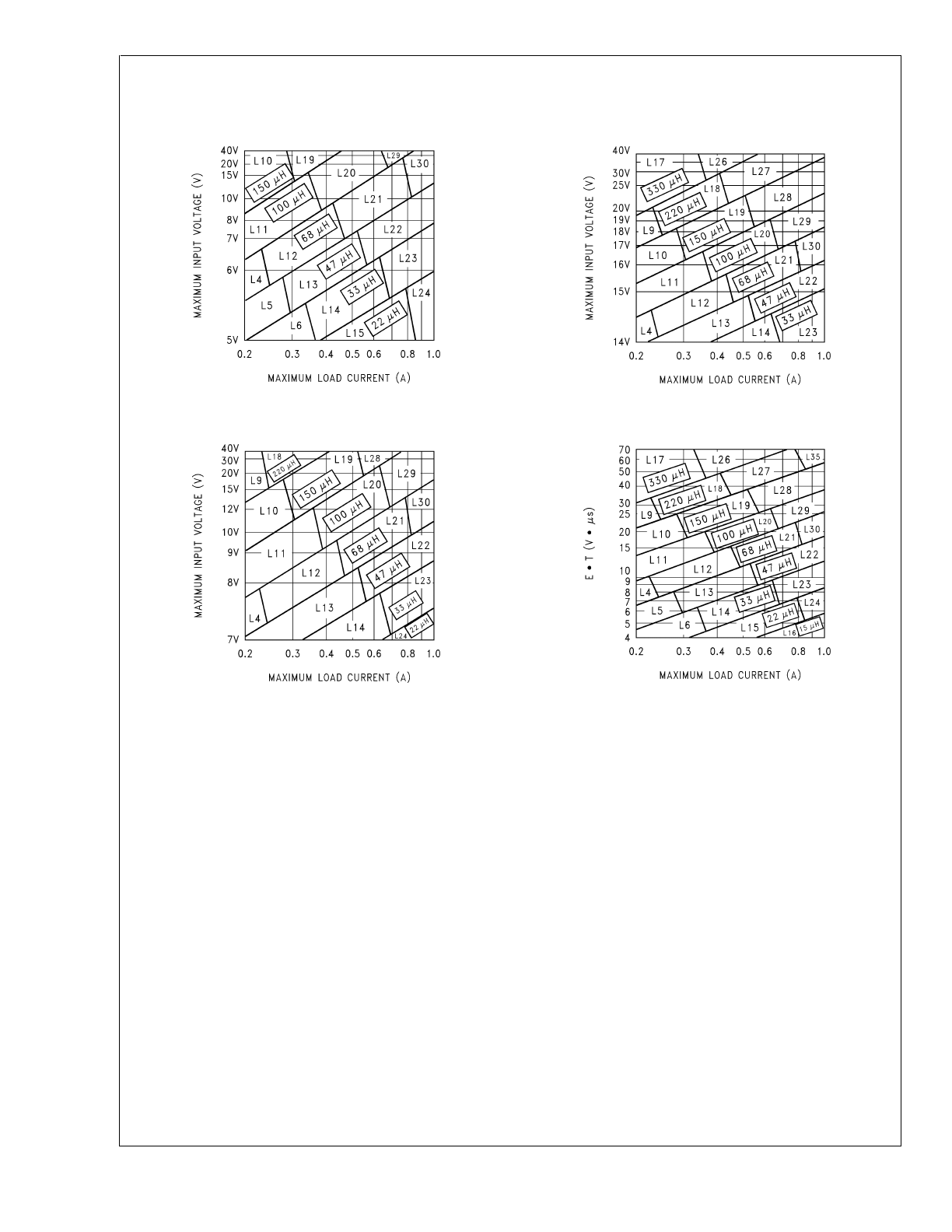
1. Inductor Selection (L1)
1. Inductor Selection (L1)
A. Select the correct inductor value selection guide from Fig-
ures
Figure 4
,
Figure 5
, or
Figure 6
(Output voltages of 3.3V,
5V, or 12V respectively.) For all other voltages, see the de-
sign procedure for the adjustable version.
A. Use the inductor selection guide for the 5V version shown
in
Figure 5
.
B. From the inductor value selection guide, identify the induc-
tance region intersected by the Maximum Input Voltage line
and the Maximum Load Current line. Each region is identified
by an inductance value and an inductor code (LXX).
B. From the inductor value selection guide shown in
Figure 5
,
the inductance region intersected by the 12V horizontal line
and the 1A vertical line is 68 µH, and the inductor code is
L30.
C. Select an appropriate inductor from the four manufactur-
er’s part numbers listed in
Figure 8
.
C. The inductance value required is 68 µH. From the table in
Figure 8
, go to the L30 line and choose an inductor part num-
ber from any of the four manufacturers shown. (In most in-
stance, both through hole and surface mount inductors are
available.)
2. Output Capacitor Selection (C
OUT
)
2. Output Capacitor Selection (C
OUT
)
A. In the majority of applications, low ESR (Equivalent Series
Resistance) electrolytic capacitors between 47 µF and 330
µF and low ESR solid tantalum capacitors between 56 µF
and 270 µF provide the best results. This capacitor should be
located close to the IC using short capacitor leads and short
copper traces. Do not use capacitors larger than 330 µF.
For additional information, see section on output capaci-
tors in application information section.
A. See section on output capacitors in application infor-
mation section.
LM2598
www.national.com
10

LM2598 Series Buck Regulator Design Procedure (Fixed Output)
(Continued)
PROCEDURE (Fixed Output Voltage Version)
EXAMPLE (Fixed Output Voltage Version)
B. To simplify the capacitor selection procedure, refer to the
quick design component selection table shown in
Figure 2
.
This table contains different input voltages, output voltages,
and load currents, and lists various inductors and output ca-
pacitors that will provide the best design solutions.
B. From the quick design component selection table shown
in
Figure 2
, locate the 5V output voltage section. In the load
current column, choose the load current line that is closest to
the current needed in your application, for this example, use
the 1A line. In the maximum input voltage column, select the
line that covers the input voltage needed in your application,
in this example, use the 15V line. Continuing on this line are
recommended inductors and capacitors that will provide the
best overall performance.
The capacitor list contains both through hole electrolytic and
surface mount tantalum capacitors from four different capaci-
tor manufacturers. It is recommended that both the manufac-
turers and the manufacturer’s series that are listed in the
table be used.
In this example aluminum electrolytic capacitors from several
different manufacturers are available with the range of ESR
numbers needed.
220 µF
25V
Panasonic HFQ Series
220 µF
25V
Nichicon PL Series
C. The capacitor voltage rating for electrolytic capacitors
should be at least 1.5 times greater than the output voltage,
and often much higher voltage ratings are needed to satisfy
the low ESR requirements for low output ripple voltage .
C. For a 5V output, a capacitor voltage rating at least 7.5V or
more is needed. But, in this example, even a low ESR,
switching grade, 220 µF 10V aluminum electrolytic capacitor
would exhibit approximately 225 m
Ω
of ESR (see the curve
in
Figure 16
for the ESR vs voltage rating). This amount of
ESR would result in relatively high output ripple voltage. To
reduce the ripple to 1% of the output voltage, or less, a ca-
pacitor with a higher voltage rating (lower ESR) should be se-
lected. A 16V or 25V capacitor will reduce the ripple voltage
by approximately half.
D. For computer aided design software, see
Switchers Made
Simple
™
(version 4.2 or later).
3. Catch Diode Selection (D1)
3. Catch Diode Selection (D1)
A. The catch diode current rating must be at least 1.3 times
greater than the maximum load current. Also, if the power
supply design must withstand a continuous output short, the
diode should have a current rating equal to the maximum
current limit of the LM2598. The most stressful condition for
this diode is an overload or shorted output condition.
A. Refer to the table shown in
Figure 11
. In this example, a
3A, 20V, 1N5820 Schottky diode will provide the best perfor-
mance, and will not be overstressed even for a shorted out-
put.
B. The reverse voltage rating of the diode should be at least
1.25 times the maximum input voltage.
C. This diode must be fast (short reverse recovery time) and
must be located close to the LM2598 using short leads and
short printed circuit traces. Because of their fast switching
speed and low forward voltage drop, Schottky diodes provide
the best performance and efficiency, and should be the first
choice, especially in low output voltage applications.
Ultra-fast recovery, or High-Efficiency rectifiers also provide
good results. Ultra-fast recovery diodes typically have re-
verse recovery times of 50 ns or less. Rectifiers such as the
1N5400 series are much too slow and should not be used.
LM2598
www.national.com
11
LM2598 Series Buck Regulator Design Procedure (Fixed Output)
(Continued)
PROCEDURE (Fixed Output Voltage Version)
EXAMPLE (Fixed Output Voltage Version)
4. Input Capacitor (C
IN
)
A low ESR aluminum or tantalum bypass capacitor is needed
between the input pin and ground to prevent large voltage
transients from appearing at the input. In addition, the RMS
current rating of the input capacitor should be selected to be
at least
1
⁄
2
the DC load current. The capacitor manufacturers
data sheet must be checked to assure that this current rating
is not exceeded. The curve shown in
Figure 15
shows typical
RMS current ratings for several different aluminum electro-
lytic capacitor values.
This capacitor should be located close to the IC using short
leads and the voltage rating should be approximately 1.5
times the maximum input voltage.
If solid tantalum input capacitors are used, it is recomended
that they be surge current tested by the manufacturer.
Use caution when using ceramic capacitors for input bypass-
ing, because it may cause severe ringing at the V
IN
pin.
For additional information, see section on input capaci-
tors in Application Information section.
4. Input Capacitor (C
IN
)
The important parameters for the Input capacitor are the in-
put voltage rating and the RMS current rating. With a nominal
input voltage of 12V, an aluminum electrolytic capacitor with
a voltage rating greater than 18V (1.5 x V
IN
) would be
needed. The next higher capacitor voltage rating is 25V.
The RMS current rating requirement for the input capacitor in
a buck regulator is approximately
1
⁄
2
the DC load current. In
this example, with a 1A load, a capacitor with a RMS current
rating of at least 500 mA is needed. The curves shown in
Fig-
ure 15
can be used to select an appropriate input capacitor.
From the curves, locate the 25V line and note which capaci-
tor values have RMS current ratings greater than 500 mA. Ei-
ther a 180 µF or 220 µF, 25V capacitor could be used.
For a through hole design, a 220 µF/25V electrolytic capaci-
tor (Panasonic HFQ series or Nichicon PL series or equiva-
lent) would be adequate. other types or other manufacturers
capacitors can be used provided the RMS ripple current rat-
ings are adequate.
For surface mount designs, solid tantalum capacitors are
recommended. The TPS series available from AVX, and the
593D series from Sprague are both surge current tested.
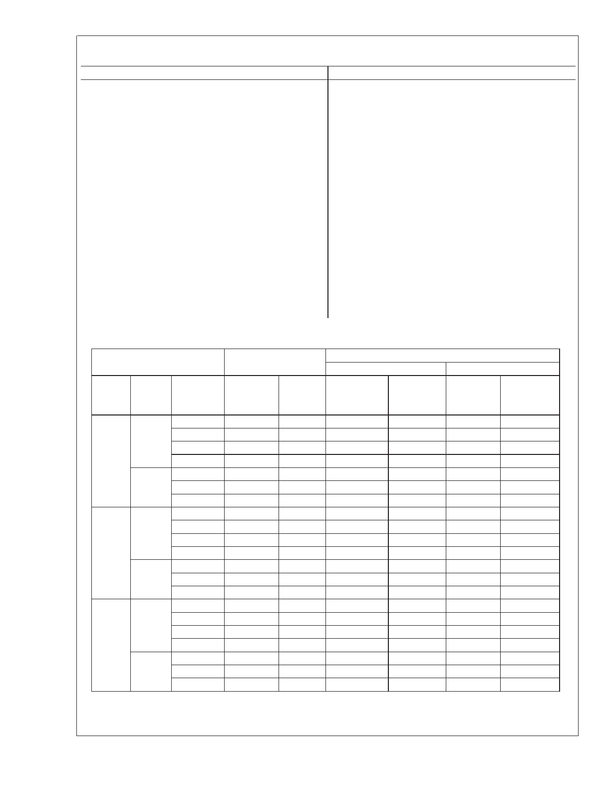
Conditions
Inductor
Output Capacitor
Through Hole Electrolytic
Surface Mount Tantalum
Output
Load
Max Input
Inductance
Inductor
Panasonic
Nichicon
AVX TPS
Sprague
Voltage
Current
Voltage
(µH)
(#)
HFQ Series
PL Series
Series
595D Series
(V)
(A)
(V)
(µF/V)
(µF/V)
(µF/V)
(µF/V)
3.3
1
5
22
L24
330/16
330/16
220/10
330/10
7
33
L23
270/25
270/25
220/10
270/10
10
47
L31
220/25
220/35
220/10
220/10
40
68
L30
180/35
220/35
220/10
180/10
6
47
L13
220/25
220/16
220/16
220/10
0.5
10
68
L21
150/35
150/25
100/16
150/16
40
100
L20
150/35
82/35
100/16
100/20
5
1
8
33
L28
330/16
330/16
220/10
270/10
10
47
L31
220/25
220/25
220/10
220/10
15
68
L30
180/35
180/35
220/10
150/16
40
100
L29
180/35
120/35
100/16
120/16
9
68
L21
180/16
180/16
220/10
150/16
0.5
20
150
L19
120/25
120/25
100/16
100/20
40
150
L19
100/25
100/25
68/20
68/25
12
1
15
47
L31
220/25
220/25
68/20
120/20
18
68
L30
180/35
120/25
68/20
120/20
30
150
L36
82/25
82/25
68/20
100/20
40
220
L35
82/25
82/25
68/20
68/25
15
68
L21
180/25
180/25
68/20
120/20
0.5
20
150
L19
82/25
82/25
68/20
100/20
40
330
L26
56/25
56/25
68/20
68/25
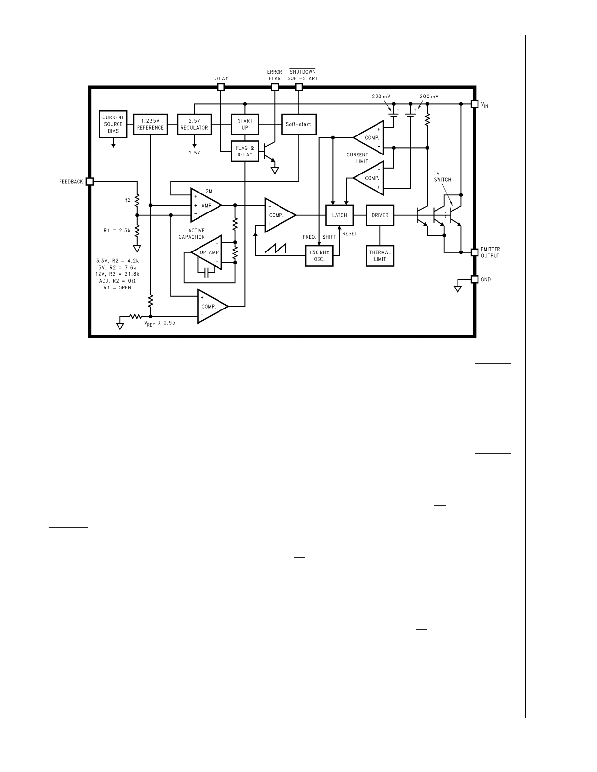
FIGURE 2. LM2598 Fixed Voltage Quick Design Component Selection Table
LM2598
www.national.com
12
LM2598 Series Buck Regulator Design Procedure (Adjustable Output)
PROCEDURE (Adjustable Output Voltage Version)
EXAMPLE (Adjustable Output Voltage Version)
Given:
V
OUT
= Regulated Output Voltage
V
IN
(max) = Maximum Input Voltage
I
LOAD
(max) = Maximum Load Current
F = Switching Frequency
(Fixed at a nominal 150 kHz).
Given:
V
OUT
= 20V
V
IN
(max) = 28V
I
LOAD
(max) = 1A
F = Switching Frequency
(Fixed at a nominal 150 kHz).
1. Programming Output Voltage (Selecting R
1
and R
2
, as
shown in
Figure 1
)
Use the following formula to select the appropriate resistor
values.
Select a value for R
1
between 240
Ω
and 1.5 k
Ω
. The lower
resistor values minimize noise pickup in the sensitive feed-
back pin. (For the lowest temperature coefficient and the best
stability with time, use 1% metal film resistors.)
1. Programming Output Voltage (Selecting R
1
and R
2
, as
shown in
Figure 1
)
Select R
1
to be 1 k
Ω
, 1%. Solve for R
2
.
R
2
= 1k (16.26 − 1) = 15.26k, closest 1% value is 15.4 k
Ω
.
R
2
= 15.4 k
Ω
.
2. Inductor Selection (L1)
A. Calculate the inductor Volt
•
microsecond constant E
•
T
(V
•
µs), from the following formula:
where V
SAT
= internal switch saturation voltage = 1V
and V
D
= diode forward voltage drop = 0.5V
2. Inductor Selection (L1)
A. Calculate the inductor Volt
•
microsecond constant
(E
•
T),
B. Use the E
•
T value from the previous formula and match
it with the E
•
T number on the vertical axis of the Inductor
Value Selection Guide shown in
Figure 7
.
B. E
•
T = 34.8 (V
•
µs)
C. on the horizontal axis, select the maximum load current.
C. I
LOAD
(max) = 1A
D. Identify the inductance region intersected by the E
•
T
value and the Maximum Load Current value. Each region is
identified by an inductance value and an inductor code
(LXX).
D. From the inductor value selection guide shown in
Figure 7
,
the inductance region intersected by the 35 (V
•
µs) horizon-
tal line and the 1A vertical line is 100 µH, and the inductor
code is L29.
E. Select an appropriate inductor from the four manufactur-
er’s part numbers listed in
Figure 8
.
E. From the table in
Figure 8
, locate line L29, and select an
inductor part number from the list of manufacturers part num-
bers.
3. Output Capacitor Selection (C
OUT
)
3. Output Capacitor SeIection (C
OUT
)
A. In the majority of applications, low ESR electrolytic or solid
tantalum capacitors between 82 µF and 220 µF provide the
best results. This capacitor should be located close to the IC
using short capacitor leads and short copper traces. Do not
use capacitors larger than 220 µF. For additional informa-
tion, see section on output capacitors in application in-
formation section.
A. See section on C
OUT
in Application Information section.
LM2598
www.national.com
13
LM2598 Series Buck Regulator Design Procedure (Adjustable Output)
(Continued)
PROCEDURE (Adjustable Output Voltage Version)
EXAMPLE (Adjustable Output Voltage Version)
B. To simplify the capacitor selection procedure, refer to the
quick design table shown in
Figure 3
. This table contains dif-
ferent output voltages, and lists various output capacitors
that will provide the best design solutions.
B. From the quick design table shown in
Figure 3
, locate the
output voltage column. From that column, locate the output
voltage closest to the output voltage in your application. In
this example, select the 24V line. Under the output capacitor
section, select a capacitor from the list of through hole elec-
trolytic or surface mount tantalum types from four different
capacitor manufacturers. It is recommended that both the
manufacturers and the manufacturers series that are listed in
the table be used.
In this example, through hole aluminum electrolytic capaci-
tors from several different manufacturers are available.
82 µF
35V
Panasonic HFQ Series
82 µF
35V
Nichicon PL Series
C. The capacitor voltage rating should be at least 1.5 times
greater than the output voltage, and often much higher volt-
age ratings are needed to satisfy the low ESR requirements
needed for low output ripple voltage.
C. For a 20V output, a capacitor rating of at least 30V or
more is needed. In this example, either a 35V or 50V capaci-
tor would work. A 35V rating was chosen although a 50V rat-
ing could also be used if a lower output ripple voltage is
needed.
Other manufacturers or other types of capacitors may also
be used, provided the capacitor specifications (especially the
100 kHz ESR) closely match the types listed in the table. Re-
fer to the capacitor manufacturers data sheet for this informa-
tion.
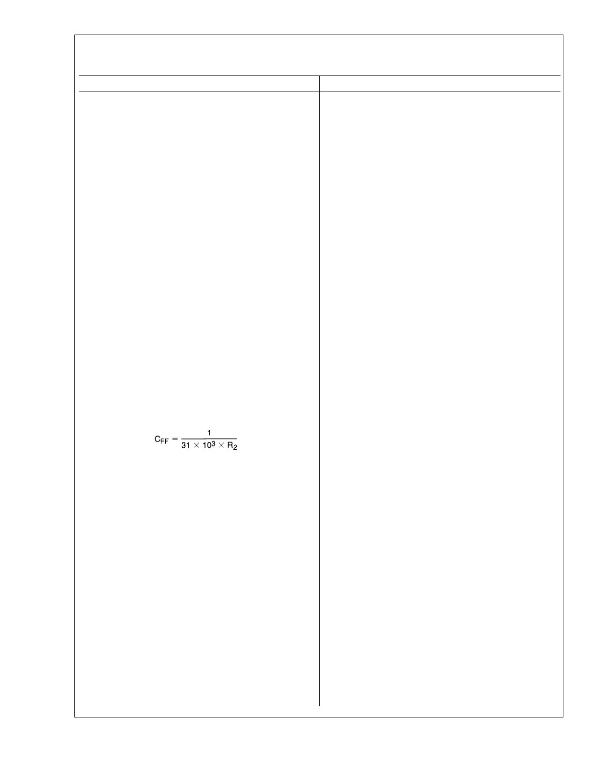
4. Feedforward Capacitor (C
FF
) (See
Figure 1
)
For output voltages greater than approximately 10V, an addi-
tional capacitor is required. The compensation capacitor is
typically between 50 pF and 10 nF, and is wired in parallel
with the output voltage setting resistor, R
2
. It provides addi-
tional stability for high output voltages, low input-output volt-
ages, and/or very low ESR output capacitors, such as solid
tantalum capacitors.
This capacitor type can be ceramic, plastic, silver mica, etc.
(Because of the unstable characteristics of ceramic capaci-
tors made with Z5U material, they are not recommended.)
4. Feedforward Capacitor (C
FF
)
The table shown in
Figure 3
contains feed forward capacitor
values for various output voltages. In this example, a 1 nF
capacitor is needed.
5. Catch Diode Selection (D1)
A. The catch diode current rating must be at least 1.3 times
greater than the maximum load current. Also, if the power
supply design must withstand a continuous output short, the
diode should have a current rating equal to the maximum
current limit of the LM2598. The most stressful condition for
this diode is an overload or shorted output condition.
B. The reverse voltage rating of the diode should be at least
1.25 times the maximum input voltage.
C. This diode must be fast (short reverse recovery time) and
must be located close to the LM2598 using short leads and
short printed circuit traces. Because of their fast switching
speed and low forward voltage drop, Schottky diodes provide
the best performance and efficiency, and should be the first
choice, especially in low output voltage applications.
Ultra-fast recovery, or High-Efficiency rectifiers are also a
good choice, but some types with an abrupt turn-off charac-
teristic may cause instability or EMl problems. Ultra-fast re-
covery diodes typically have reverse recovery times of 50 ns
or less. Rectifiers such as the 1N4001 series are much too
slow and should not be used.
5. Catch Diode Selection (D1)
A. Refer to the table shown in
Figure 11
. Schottky diodes
provide the best performance, and in this example a 3A, 40V,
1N5822 Schottky diode would be a good choice. The 3A di-
ode rating is more than adequate and will not be over-
stressed even for a shorted output.
LM2598
www.national.com
14
LM2598 Series Buck Regulator Design Procedure (Adjustable Output)
(Continued)
PROCEDURE (Adjustable Output Voltage Version)
EXAMPLE (Adjustable Output Voltage Version)
6. Input Capacitor (C
IN
)
A low ESR aluminum or tantalum bypass capacitor is needed
between the input pin and ground to prevent large voltage
transients from appearing at the input. In addition, the RMS
current rating of the input capacitor should be selected to be
at least
1
⁄
2
the DC load current. The capacitor manufacturers
data sheet must be checked to assure that this current rating
is not exceeded. The curve shown in
Figure 15
shows typical
RMS current ratings for several different aluminum electro-
lytic capacitor values.
This capacitor should be located close to the IC using short
leads and the voltage rating should be approximately 1.5
times the maximum input voltage.
If solid tantalum input capacitors are used, it is recomended
that they be surge current tested by the manufacturer.
Use caution when using a high dielectric constant ceramic
capacitor for input bypassing, because it may cause severe
ringing at the V
IN
pin.
6. Input Capacitor (C
IN
)
The important parameters for the Input capacitor are the in-
put voltage rating and the RMS current rating. With a nominal
input voltage of 28V, an aluminum electrolytic aluminum elec-
trolytic capacitor with a voltage rating greater than 42V (1.5 x
V
IN
) would be needed. Since the the next higher capacitor
voltage rating is 50V, a 50V capacitor should be used. The
capacitor voltage rating of (1.5 x V
IN
) is a conservative guide-
line, and can be modified somewhat if desired.
The RMS current rating requirement for the input capacitor of
a buck regulator is approximately
1
⁄
2
the DC load current. In
this example, with a 1A load, a capacitor with a RMS current
rating of at least 500 mA is needed.
The curves shown in
Figure 15
can be used to select an ap-
propriate input capacitor. From the curves, locate the 50V
line and note which capacitor values have RMS current rat-
ings greater than 500 mA. Either a 100 µF or 120 µF, 50V ca-
pacitor could be used.
For a through hole design, a 120 µF/50V electrolytic capaci-
tor (Panasonic HFQ series or Nichicon PL series or equiva-
lent) would be adequate. Other types or other manufacturers
capacitors can be used provided the RMS ripple current rat-
ings are adequate.
For surface mount designs, solid tantalum capacitors can be
used, but caution must be exercised with regard to the ca-
pacitor surge current rating (see Application Information or
input capacitors in this data sheet). The TPS series available
from AVX, and the 593D series from Sprague are both surge
current tested.
For additional information, see section on input capaci-
tor in application information section.
To further simplify the buck regulator design procedure, Na-
tional Semiconductor is making available computer design
software to be used with the Simple Switcher line ot switch-
ing regulators. Switchers Made Simple (version 4.2 or later)
is available on a 3
1
⁄
2
" diskette for IBM compatible computers.
Output
Voltage
(V)
Through Hole Electrolytic Output Capacitor
Surface Mount Tantalum Output Capacitor
Panasonic
Nichicon PL
Feedforward
AVX TPS
Sprague
Feedforward
HFQ Series
Series
Capacitor
Series
595D Series
Capacitor
(µF/V)
(µF/V)
(µF/V)
(µF/V)
1.2
330/50
330/50
0
330/6.3
330/6.3
0
4
220/25
220/25
4.7 nF
220/10
220/10
4.7 nF
6
220/25
220/25
3.3 nF
220/10
220/10
3.3 nF
9
180/25
180/25
1.5 nF
100/16
180/16
1.5 nF
1 2
120/25
120/25
1.5 nF
68/20
120/20
1.5 nF
1 5
120/25
120/25
1.5 nF
68/20
100/20
1.5 nF
2 4
82/35
82/35
1 nF
33/25
33/35
220 pF
2 8
82/50
82/50
1 nF
10/35
33/35
220 pF
FIGURE 3. Output Capacitor and Feedforward Capacitor Selection Table
LM2598
www.national.com
15
LM2598 Series Buck Regulator Design Procedure
INDUCTOR VALUE SELECTION GUIDES (For Continuous Mode Operation)
DS012593-25
FIGURE 4. LM2598-3.3
DS012593-26
FIGURE 5. LM2598-5.0
DS012593-27
FIGURE 6. LM2598-12
DS012593-28
FIGURE 7. LM2598-ADJ
LM2598
www.national.com
16
LM2598 Series Buck Regulator Design Procedure
(Continued)
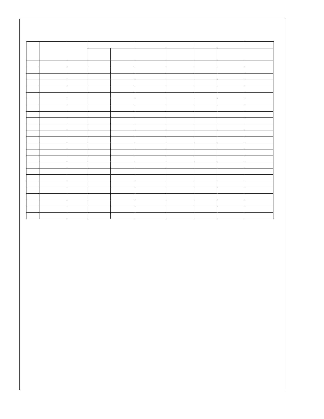
Inductance
(µH)
Current
(A)
Schott
Renco
Pulse Engineering
Coilcraft
Through
Surface
Through
Surface
Through
Surface
Surface
Hole
Mount
Hole
Mount
Hole
Mount
Mount
L4
68
0.32
67143940
67144310
RL-1284-68-43
RL1500-68
PE-53804
PE-53804-S
DO1608-68
L5
47
0.37
67148310
67148420
RL-1284-47-43
RL1500-47
PE-53805
PE-53805-S
DO1608-473
L6
33
0.44
67148320
67148430
RL-1284-33-43
RL1500-33
PE-53806
PE-53806-S
DO1608-333
L9
220
0.32
67143960
67144330
RL-5470-3
RL1500-220
PE-53809
PE-53809-S
DO3308-224
L10
150
0.39
67143970
67144340
RL-5470-4
RL1500-150
PE-53810
PE-53810-S
DO3308-154
L11
100
0.48
67143980
67144350
RL-5470-5
RL1500-100
PE-53811
PE-53811-S
DO3308-104
L12
68
0.58
67143990
67144360
RL-5470-6
RL1500-68
PE-53812
PE-53812-S
DO3308-683
L13
47
0.70
67144000
67144380
RL-5470-7
RL1500-47
PE-53813
PE-53813-S
DO3308-473
L14
33
0.83
67148340
67148450
RL-1284-33-43
RL1500-33
PE-53814
PE-53814-S
DO3308-333
L15
22
0.99
67148350
67148460
RL-1284-22-43
RL1500-22
PE-53815
PE-53815-S
DO3308-223
L16
15
1.24
67148360
67148470
RL-1284-15-43
RL1500-15
PE-53816
PE-53816-S
DO3308-153
L17
330
0.42
67144030
67144410
RL-5471-1
RL1500-330
PE-53817
PE-53817-S
DO3316-334
L18
220
0.55
67144040
67144420
RL-5471-2
RL1500-220
PE-53818
PE-53818-S
DO3316-224
L19
150
0.66
67144050
67144430
RL-5471-3
RL1500-150
PE-53819
PE-53819-S
DO3316-154
L20
100
0.82
67144060
67144440
RL-5471-4
RL1500-100
PE-53820
PE-53820-S
DO3316-104
L21
68
0.99
67144070
67144450
RL-5471-5
RL1500-68
PE-53821
PE-53821-S
DO3316-683
L22
47
1.17
67144080
67144460
RL-5471-6
—
PE-53822
PE-53822-S
DO3316-473
L23
33
1.40
67144090
67144470
RL-5471-7
—
PE-53823
PE-53823-S
DO3316-333
L24
22
1.70
67148370
67144480
RL-1283-22-43
—
PE-53824
PE-53824-S
DO3316-223
L26
330
0.80
67144100
67144480
RL-5471-1
—
PE-53826
PE-53826-S
DO5022P-334
L27
220
1.00
67144110
67144490
RL-5471-2
—
PE-53827
PE-53827-S
DO5022P-224
L28
150
1.20
67144120
67144500
RL-5471-3
—
PE-53828
PE-53828-S
DO5022P-154
L29
100
1.47
67144130
67144510
RL-5471-4
—
PE-53829
PE-53829-S
DO5022P-104
L30
68
1.78
67144140
67144520
RL-5471-5
—
PE-53830
PE-53830-S
DO5022P-683
L35
47
2.15
67144170
—
RL-5473-1
—
PE-53935
PE-53935-S
—
FIGURE 8. Inductor Manufacturers Part Numbers
LM2598
www.national.com
17
LM2598 Series Buck Regulator Design Procedure
(Continued)
Coilcraft Inc.
Phone
(800) 322-2645
FAX
(708) 639-1469
Coilcraft Inc., Europe
Phone
+11 1236 730
595
FAX
+44 1236 730
627
Pulse Engineering Inc.
Phone
(619) 674-8100
FAX
(619) 674-8262
Pulse Engineering Inc.,
Phone
+353 93 24 107
Europe
FAX
+353 93 24 459
Renco Electronics Inc.
Phone
(800) 645-5828
FAX
(516) 586-5562
Schott Corp.
Phone
(612) 475-1173
FAX
(612) 475-1786
FIGURE 9. Inductor Manufacturers Phone Numbers
Nichicon Corp.
Phone
(708) 843-7500
FAX
(708) 843-2798
Panasonic
Phone
(714) 373-7857
FAX
(714) 373-7102
AVX Corp.
Phone
(803) 448-9411
FAX
(803) 448-1943
Sprague/Vishay
Phone
(207) 324-4140
FAX
(207) 324-7223
FIGURE 10. Capacitor Manufacturers Phone Numbers
VR
1A Diodes
3A Diodes
Surface Mount
Through Hole
Surface Mount
Through Hole
Schottky
Ultra Fast
Schottky
Ultra Fast
Schottky
Ultra Fast
Schottky
Ultra Fast
Recovery
Recovery
Recovery
Recovery
20V
SK12
All of these
1N5817
All of these
All of these
IN5820
All of these
diodes are
SR102
diodes are
SK32
diodes are
SR302
diodes are
rated to at
rated to at
rated to at
MBR320
rated to at
30V
SK13
least 50V.
1N5818
least 50V.
least 50V.
1N5821
least 50V.
MBRS130
SR103
SK33
MBR330
11DQ03
31DQ03
40V
SK14
1N5822
MBRS140
1N5819
SK34
SR304
10BQ040
SR104
MBRS340
MBR340
10MQ040
MURS120
11DQ04
MUR120
30WQ04
MURS320
31DQ04
MUR320
50V
or
more
MBRS160
10BF10
SR105
SK35
30WF10
SR305
30WF10
10BQ050
MBR150
MBRS360
MBR350
10MQ060
11DQ05
30WQ05
31DQ05
FIGURE 11. Diode Selection Table
LM2598
www.national.com
18
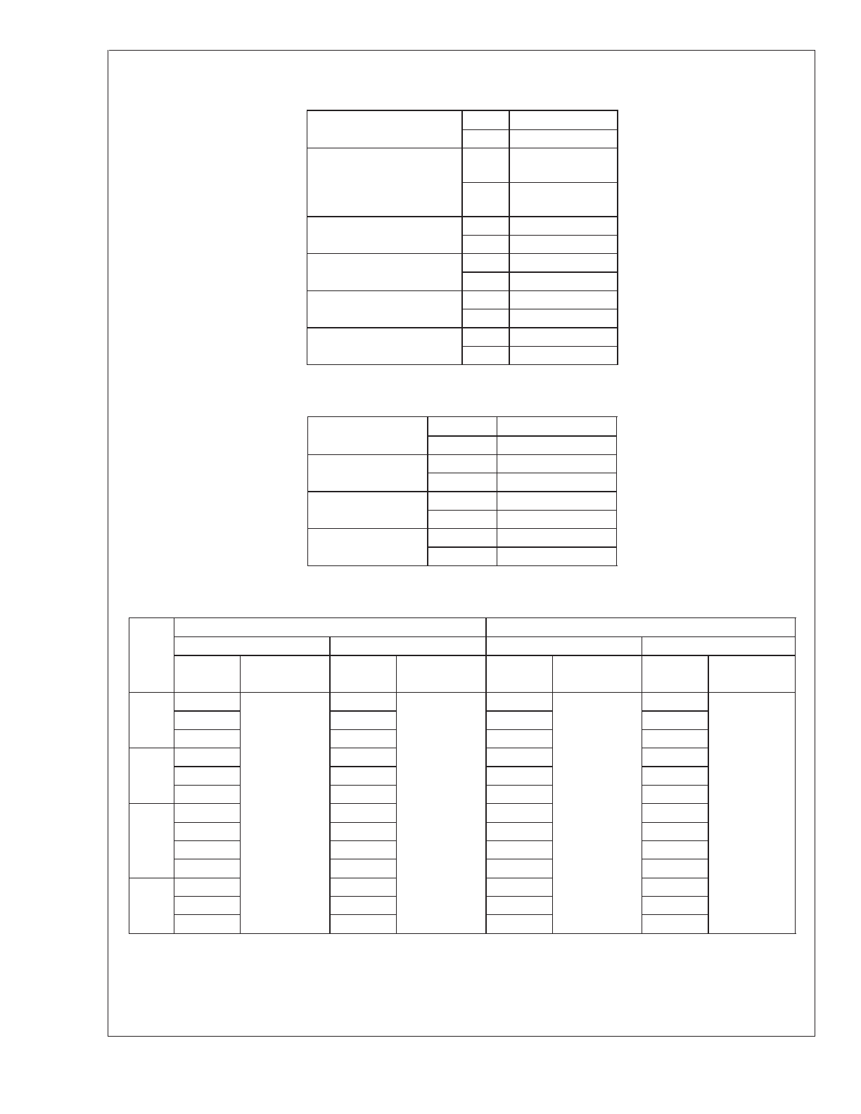
Block Diagram
Application Information
PIN FUNCTIONS
+V
IN
(Pin 2) — This is the positive input supply for the IC
switching regulator. A suitable input bypass capacitor must
be present at this pin to minimize voltage transients and to
supply the switching currents needed by the regulator.
Ground (Pin 4) — Circuit ground.
Output (Pin 1) — Internal switch. The voltage at this pin
switches between approximately (+V
IN
− V
SAT
) and approxi-
mately −0.5V, with a duty cycle of V
OUT
/V
IN
. To minimize
coupling to sensitive circuitry, the PC board copper area con-
nected to this pin should be kept to a minimum.
Feedback (Pin 6) — Senses the regulated output voltage to
complete the feedback loop.
Shutdown /Soft-start (Pin 7) — This dual function pin pro-
vides the following features: (a) Allows the switching regula-
tor circuit to be shut down using logic level signals thus drop-
ping the total input supply current to approximately 85 µA.
(b) Adding a capacitor to this pin provides a soft-start feature
which minimizes startup current and provides a controlled
ramp up of the output voltage.
Error Flag (Pin 3) — Open collector output that provides a
low signal (flag transistor ON) when the regulated output
voltage drops more than 5% from the nominal output volt-
age. On start up, Error Flag is low until V
OUT
reaches 95% of
the nominal output voltage and a delay time determined by
the Delay pin capacitor. This signal can be used as a reset to
a microprocessor on power-up.
Delay (Pin 5) — At power-up, this pin can be used to provide
a time delay between the time the regulated output voltage
reaches 95% of the nominal output voltage, and the time the
error flag output goes high.
Special Note If any of the above three features (Shutdown
/Soft-start, Error Flag, or Delay) are not used, the respective
pins should be left open.
EXTERNAL COMPONENTS
SOFT-START CAPACITOR
C
SS
— A capacitor on this pin provides the regulator with a
Soft-start feature (slow start-up). When the DC input voltage
is first applied to the regulator, or when the Shutdown
/Soft-start pin is allowed to go high, a constant current (ap-
proximately 5 µA begins charging this capacitor). As the ca-
pacitor voltage rises, the regulator goes through four operat-
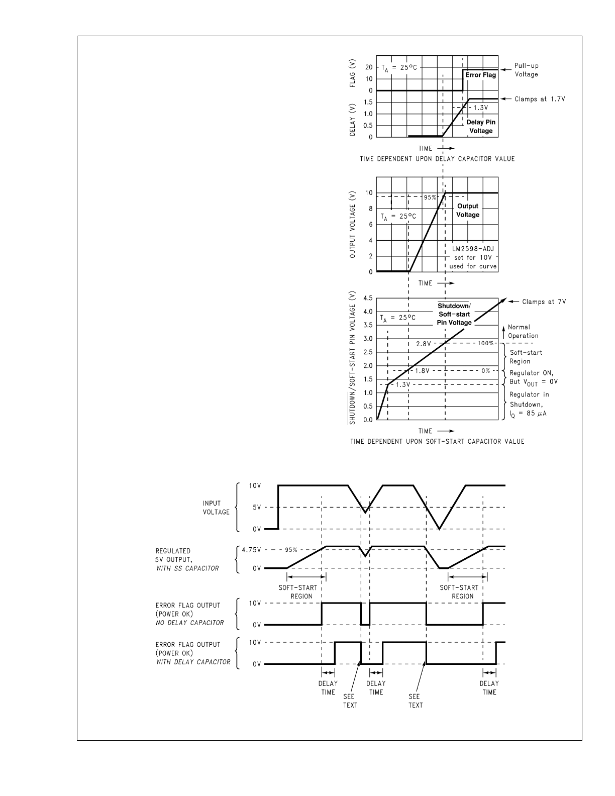
ing regions (See the bottom curve in
Figure 13
).
1. Regulator in Shutdown.
When the SD /SS pin voltage is
between 0V and 1.3V, the regulator is in shutdown, the out-
put voltage is zero, and the IC quiescent current is approxi-
mately 85 µA.
2. Regulator ON, but the output voltage is zero.
With the
SD /SS pin voltage between approximately 1.3V and 1.8V,
the internal regulator circuitry is operating, the quiescent cur-
rent rises to approximately 5 mA, but the output voltage is
still zero. Also, as the 1.3V threshold is exceeded, the
Soft-start capacitor charging current decreases from 5 µA
down to approximately 1.6 µA. This decreases the slope of
capacitor voltage ramp.
3. Soft-start Region.
When the SD /SS pin voltage is be-
tween 1.8V and 2.8V (
@
25˚C), the regulator is in a Soft-start
condition. The switch (Pin 1) duty cycle initially starts out
very low, with narrow pulses and gradually get wider as the
capacitor SD /SS pin ramps up towards 2.8V. As the duty
cycle increases, the output voltage also increases at a con-
trolled ramp up. See the center curve in
Figure 13
. The input
supply current requirement also starts out at a low level for
DS012593-29
FIGURE 12.
LM2598
www.national.com
19
Application Information
(Continued)
the narrow pulses and ramp up in a controlled manner. This
is a very useful feature in some switcher topologies that re-
quire large startup currents (such as the inverting configura-
tion) which can load down the input power supply.
Note: The lower curve shown in
Figure 13 shows the Soft-start region from
0% to 100%. This is not the duty cycle percentage, but the output volt-
age percentage. Also, the Soft-start voltage range has a negative tem-
perature coefficient associated with it. See the Soft-start curve in the
electrical characteristics section.
4. Normal operation.
Above 2.8V, the circuit operates as a
standard Pulse Width Modulated switching regulator. The
capacitor will continue to charge up until it reaches the inter-
nal clamp voltage of approximately 7V. If this pin is driven
from a voltage source, the current must be limited to about
1 mA.
DS012593-30
FIGURE 13. Soft-start, Delay, Error, Output
DS012593-31
FIGURE 14. Timing Diagram for 5V Output
LM2598
www.national.com
20
Application Information
(Continued)
DELAY CAPACITOR
C
DELAY
— Provides delay for the error flag output. See the
upper curve in
Figure 13
, and also refer to timing diagrams in
Figure 14
. A capacitor on this pin provides a time delay be-
tween the time the regulated output voltage (when it is in-
creasing in value) reaches 95% of the nominal output volt-
age, and the time the error flag output goes high. A 3 µA
constant current from the delay pin charges the delay ca-
pacitor resulting in a voltage ramp. When this voltage
reaches a threshold of approximately 1.3V, the open collec-
tor error flag output (or power OK) goes high. This signal can
be used to indicate that the regulated output has reached the
correct voltage and has stabilized.
If, for any reason, the regulated output voltage drops by 5%
or more, the error output flag (Pin 3) immediately goes low
(internal transistor turns on). The delay capacitor provides
very little delay if the regulated output is dropping out of
regulation. The delay time for an output that is decreasing is
approximately a 1000 times less than the delay for the rising
output. For a 0.1 µF delay capacitor, the delay time would be
approximately 50 ms when the output is rising and passes
through the 95% threshold, but the delay for the output drop-
ping would only be approximately 50 µs.
R
Pull Up
— The error flag output, (or power OK) is the collec-
tor of a NPN transistor, with the emitter internally grounded.
To use the error flag, a pullup resistor to a positive voltage is
needed. The error flag transistor is rated up to a maximum of
45V and can sink approximately 3 mA. If the error flag is not
used, it can be left open.
FEEDFORWARD CAPACITOR
(Adjustable Output Voltage Version)
C
FF
— A Feedforward Capacitor C
FF
, shown across R2 in
Figure 1
is used when the output voltage is greater than 10V
or then C
OUT
has a very low ESR. This capacitor adds lead
compensation to the feedback loop and increases the phase
margin for better loop stability. For C
FF
selection, see the de-
sign procedure section.
If the output ripple is large (
>
5% of the nominal output volt-
age), this ripple can be coupled to the feedback pin through
the feedforward capacitor and cause the error comparator to
trigger the error flag. In this situation, adding a resistor, R
FF
,
in series with the feedforward capacitor, approximately 3
times R1, will attenuate the ripple voltage at the feedback
pin.
INPUT CAPACITOR
C
IN
— A low ESR aluminum or tantalum bypass capacitor is
needed between the input pin and ground pin. It must be lo-
cated near the regulator using short leads. This capacitor
prevents large voltage transients from appearing at the in-
put, and provides the instantaneous current needed each
time the switch turns on.
The important parameters for the Input capacitor are the
voltage rating and the RMS current rating. Because of the
relatively high RMS currents flowing in a buck regulator’s in-
put capacitor, this capacitor should be chosen for its RMS
current rating rather than its capacitance or voltage ratings,
although the capacitance value and voltage rating are di-
rectly related to the RMS current rating.
The RMS current rating of a capacitor could be viewed as a
capacitor’s power rating. The RMS current flowing through
the capacitors internal ESR produces power which causes
the internal temperature of the capacitor to rise. The RMS
current rating of a capacitor is determined by the amount of
current required to raise the internal temperature approxi-
mately 10˚C above an ambient temperature of 105˚C. The
ability of the capacitor to dissipate this heat to the surround-
ing air will determine the amount of current the capacitor can
safely sustain. Capacitors that are physically large and have
a large surface area will typically have higher RMS current
ratings. For a given capacitor value, a higher voltage electro-
lytic capacitor will be physically larger than a lower voltage
capacitor, and thus be able to dissipate more heat to the sur-
rounding air, and therefore will have a higher RMS current
rating.
The consequences of operating an electrolytic capacitor
above the RMS current rating is a shortened operating life.
The higher temperature speeds up the evaporation of the ca-
pacitor’s electrolyte, resulting in eventual failure.
Selecting an input capacitor requires consulting the manu-
facturers data sheet for maximum allowable RMS ripple cur-
rent. For a maximum ambient temperature of 40˚C, a gen-
eral guideline would be to select a capacitor with a ripple
current rating of approximately 50% of the DC load current.
For ambient temperatures up to 70˚C, a current rating of
75% of the DC load current would be a good choice for a
conservative design. The capacitor voltage rating must be at
least 1.25 times greater than the maximum input voltage,
and often a much higher voltage capacitor is needed to sat-
isfy the RMS current requirements.
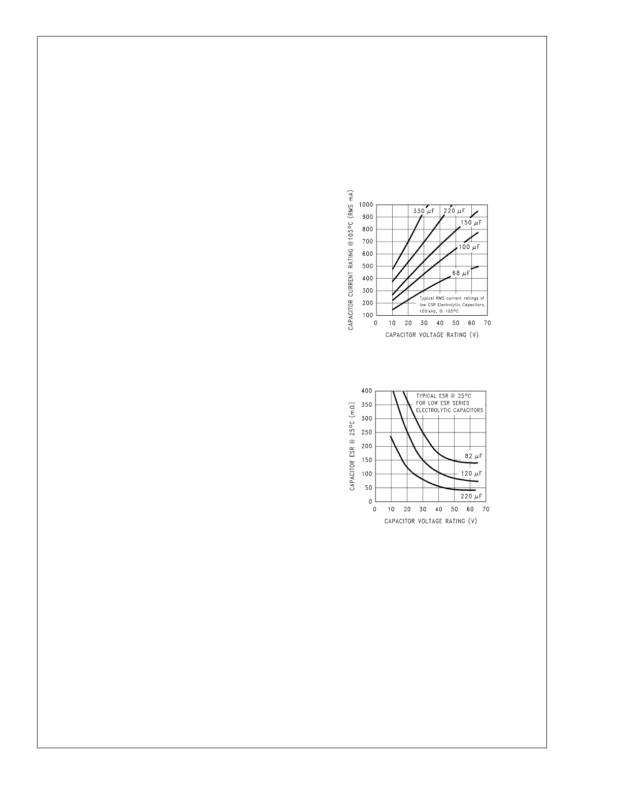
DS012593-32
FIGURE 15. RMS Current Ratings for Low
ESR Electrolytic Capacitors (Typical)
DS012593-33
FIGURE 16. Capacitor ESR vs Capacitor Voltage Rating
(Typical Low ESR Electrolytic Capacitor)
LM2598
www.national.com
21
Application Information
(Continued)
A graph shown in
Figure 15
shows the relationship between
an electrolytic capacitor value, its voltage rating, and the
RMS current it is rated for. These curves were obtained from
the Nichicon “PL” series of low ESR, high reliability electro-
lytic capacitors designed for switching regulator applications.
Other capacitor manufacturers offer similar types of capaci-
tors, but always check the capacitor data sheet.
“Standard” electrolytic capacitors typically have much higher
ESR numbers, lower RMS current ratings and typically have
a shorter operating lifetime.
Because of their small size and excellent performance, sur-
face mount solid tantalum capacitors are often used for input
bypassing, but several precautions must be observed. A
small percentage of solid tantalum capacitors can short if the
inrush current rating is exceeded. This can happen at turn on
when the input voltage is suddenly applied, and of course,
higher input voltages produce higher inrush currents. Sev-
eral capacitor manufacturers do a 100% surge current test-
ing on their products to minimize this potential problem. If
high turn on currents are expected, it may be necessary to
limit this current by adding either some resistance or induc-
tance before the tantalum capacitor, or select a higher volt-
age capacitor. As with aluminum electrolytic capacitors, the
RMS ripple current rating must be sized to the load current.
OUTPUT CAPACITOR
C
OUT
— An output capacitor is required to filter the output
and provide regulator loop stability. Low impedance or low
ESR Electrolytic or solid tantalum capacitors designed for
switching regulator applications must be used. When select-
ing an output capacitor, the important capacitor parameters
are; the 100 kHz Equivalent Series Resistance (ESR), the
RMS ripple current rating, voltage rating, and capacitance
value. For the output capacitor, the ESR value is the most
important parameter.
The output capacitor requires an ESR value that has an up-
per and lower limit. For low output ripple voltage, a low ESR
value is needed. This value is determined by the maximum
allowable output ripple voltage, typically 1% to 2% of the out-
put voltage. But if the selected capacitor’s ESR is extremely
low, there is a possibility of an unstable feedback loop, re-
sulting in an oscillation at the output. Using the capacitors
listed in the tables, or similar types, will provide design solu-
tions under all conditions.
If very low output ripple voltage (less than 15 mV) is re-
quired, refer to the section on Output Voltage Ripple and
Transients for a post ripple filter.
An aluminum electrolytic capacitor’s ESR value is related to
the capacitance value and its voltage rating. In most cases,
higher voltage electrolytic capacitors have lower ESR values
(see
Figure 16
). Often, capacitors with much higher voltage
ratings may be needed to provide the low ESR values re-
quired for low output ripple voltage.
The output capacitor for many different switcher designs of-
ten can be satisfied with only three or four different capacitor
values and several different voltage ratings. See the quick
design component selection tables in
Figure 2
and
Figure 3
for typical capacitor values, voltage ratings, and manufactur-
ers capacitor types.
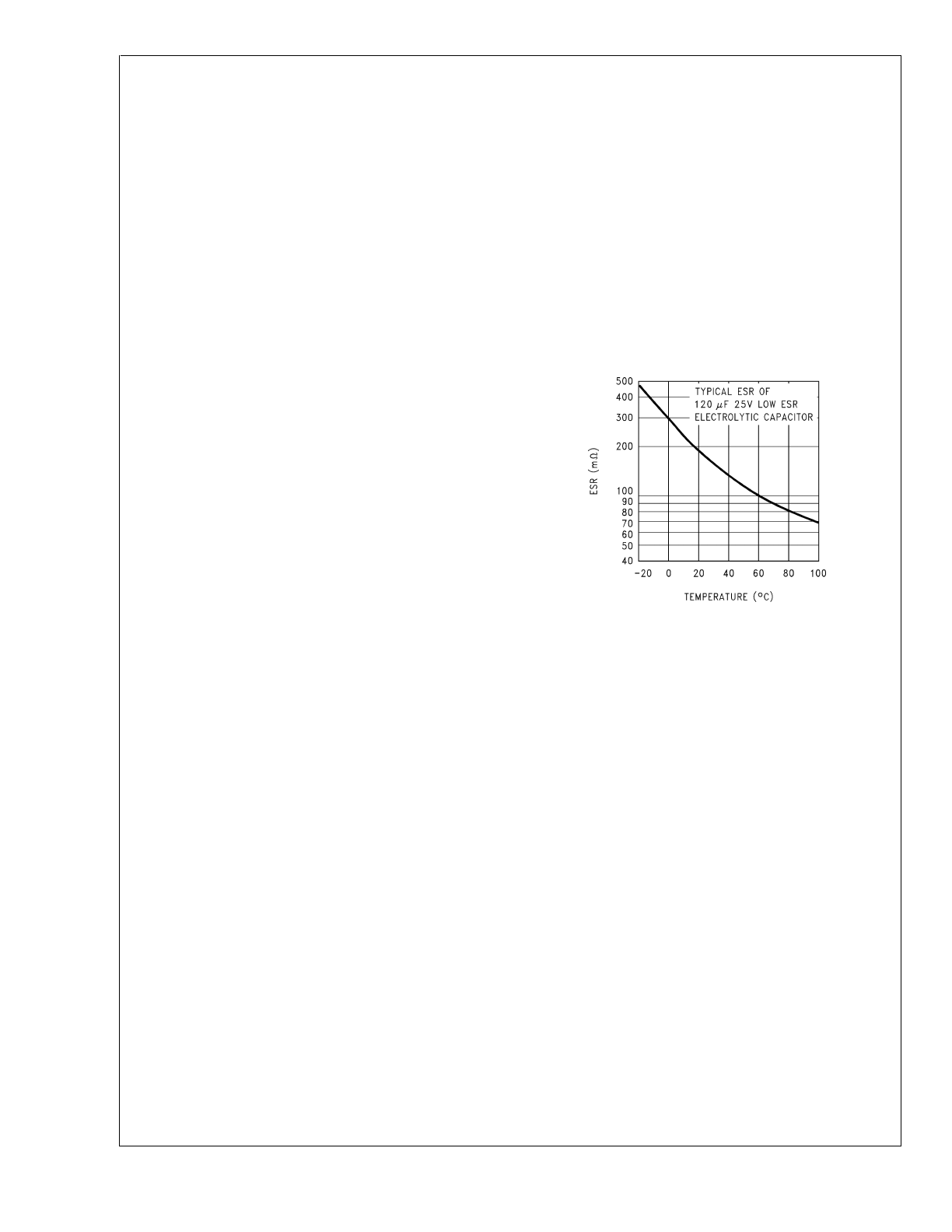
Electrolytic capacitors are not recommended for tempera-
tures below −25˚C. The ESR rises dramatically at cold tem-
peratures and typically rises 3X
@
−25˚C and as much as
10X at −40˚C. See curve shown in
Figure 17
.
Solid tantalum capacitors have a much better ESR spec for
cold temperatures and are recommended for temperatures
below −25˚C.
CATCH DIODE
Buck regulators require a diode to provide a return path for
the inductor current when the switch turns off. This must be
a fast diode and must be located close to the LM2598 using
short leads and short printed circuit traces.
Because of their very fast switching speed and low forward
voltage drop, Schottky diodes provide the best performance,
especially in low output voltage applications (5V and lower).
Ultra-fast recovery, or High-Efficiency rectifiers are also a
good choice, but some types with an abrupt turnoff charac-
teristic may cause instability or EMI problems. Ultra-fast re-
covery diodes typically have reverse recovery times of 50 ns
or less. Rectifiers such as the 1N5400 series are much too
slow and should not be used.
INDUCTOR SELECTION
All switching regulators have two basic modes of operation;
continuous and discontinuous. The difference between the
two types relates to the inductor current, whether it is flowing
continuously, or if it drops to zero for a period of time in the
normal switching cycle. Each mode has distinctively different
operating characteristics, which can affect the regulators
performance and requirements. Most switcher designs will
operate in the discontinuous mode when the load current is
low.
The LM2598 (or any of the Simple Switcher family) can be
used for both continuous or discontinuous modes of opera-
tion.
In many cases the preferred mode of operation is the con-
tinuous mode. It offers greater output power, lower peak
switch, inductor and diode currents, and can have lower out-
put ripple voltage. But it does require larger inductor values
to keep the inductor current flowing continuously, especially
at low output load currents and/or high input voltages.
To simplify the inductor selection process, an inductor selec-
tion guide (nomograph) was designed (see
Figure 3
through
Figure 6
). This guide assumes that the regulator is operating
in the continuous mode, and selects an inductor that will al-
low a peak-to-peak inductor ripple current to be a certain
percentage of the maximum design load current. This
peak-to-peak inductor ripple current percentage is not fixed,
but is allowed to change as different design load currents are
selected. (See
Figure 18
.)
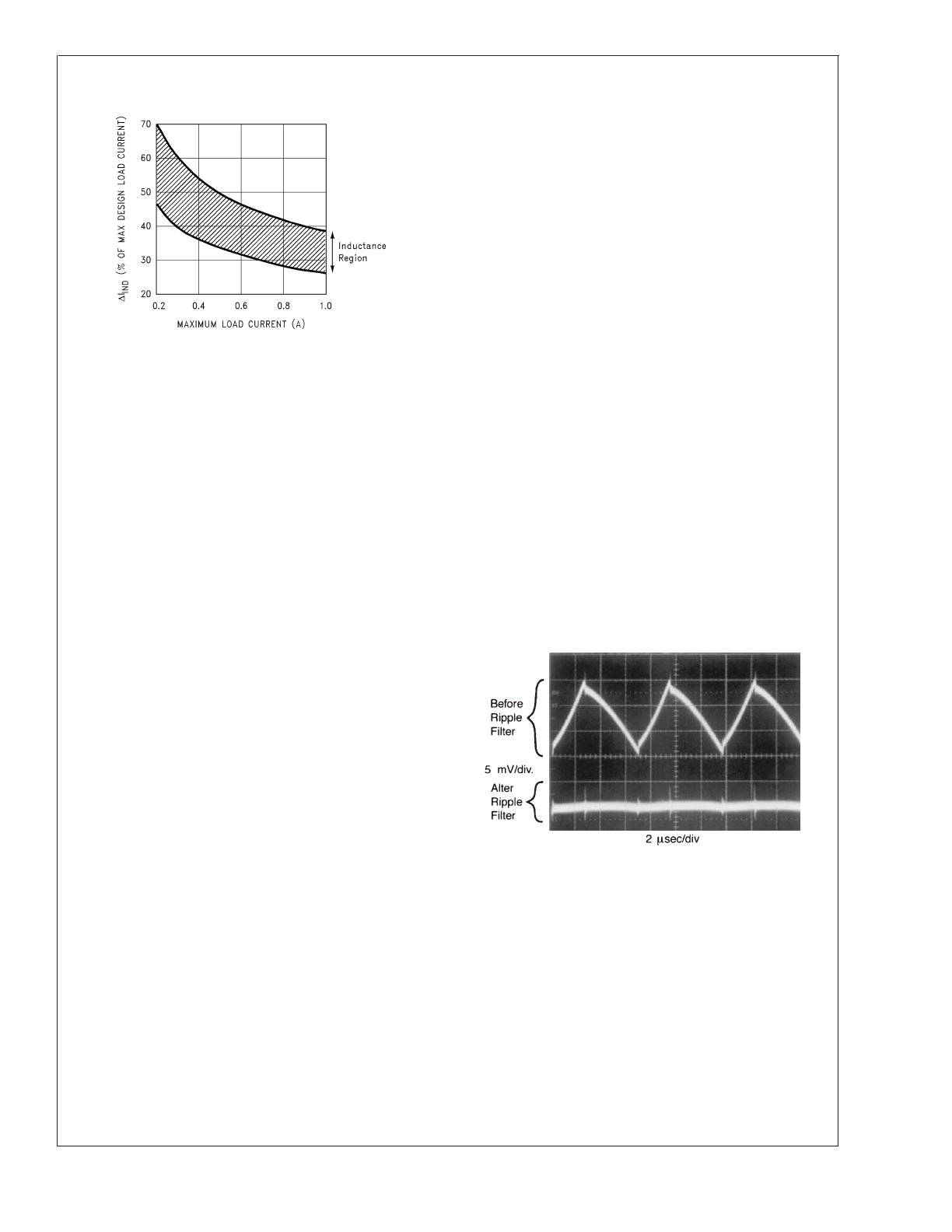
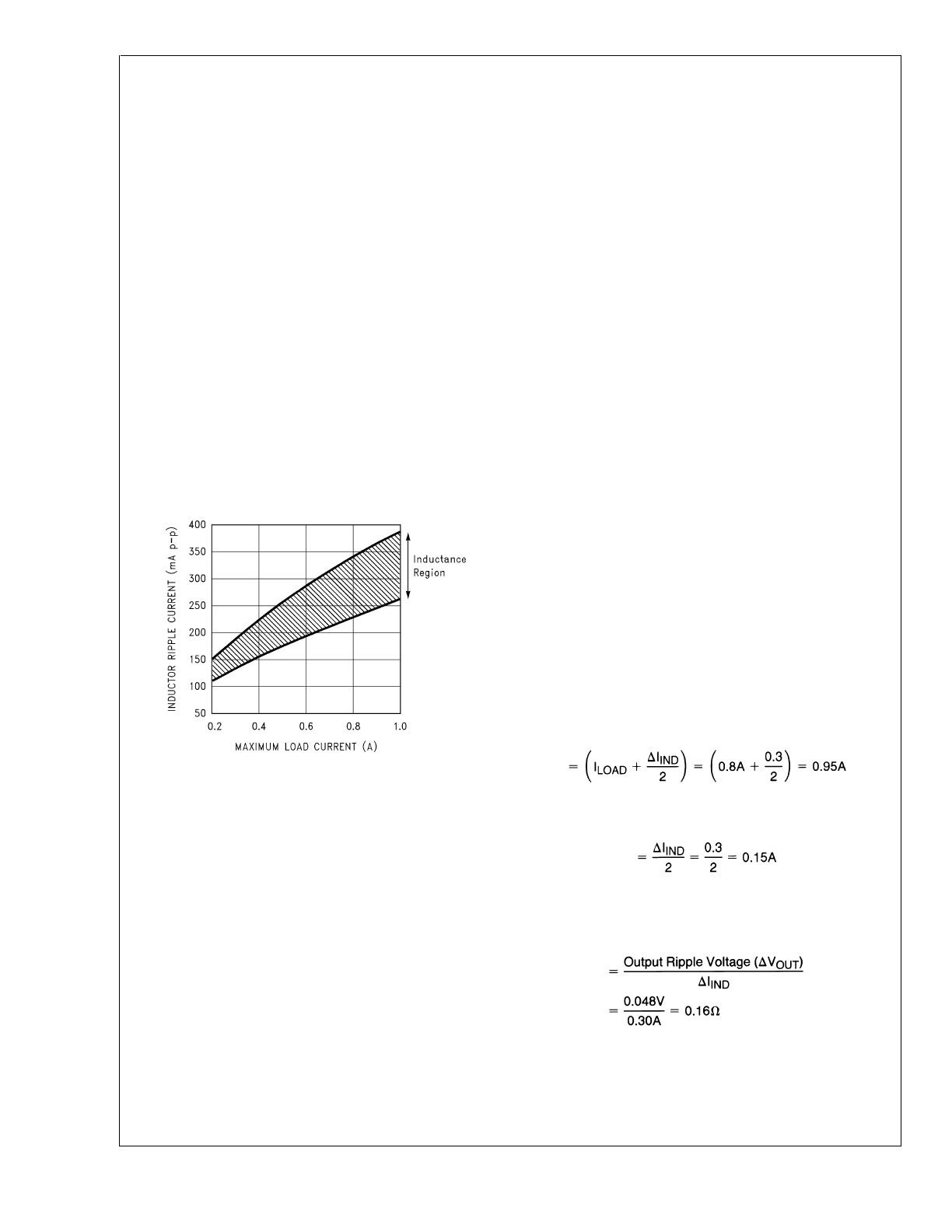
DS012593-34
FIGURE 17. Capacitor ESR Change vs Temperature
LM2598
www.national.com
22
Application Information
(Continued)
By allowing the percentage of inductor ripple current to in-
crease for low load currents, the inductor value and size can
be kept relatively low.
When operating in the continuous mode, the inductor current
waveform ranges from a triangular to a sawtooth type of
waveform (depending on the input voltage), with the average
value of this current waveform equal to the DC output load
current.
Inductors are available in different styles such as pot core,
toroid, E-core, bobbin core, etc., as well as different core ma-
terials, such as ferrites and powdered iron. The least expen-
sive, the bobbin, rod or stick core, consists of wire wound on
a ferrite bobbin. This type of construction makes for an inex-
pensive inductor, but since the magnetic flux is not com-
pletely contained within the core, it generates more
Electro-Magnetic Interference (EMl). This magnetic flux can
induce voltages into nearby printed circuit traces, thus caus-
ing problems with both the switching regulator operation and
nearby sensitive circuitry, and can give incorrect scope read-
ings because of induced voltages in the scope probe. Also
see section on Open Core Inductors.
When multiple switching regulators are located on the same
PC board, open core magnetics can cause interference be-
tween two or more of the regulator circuits, especially at high
currents. A torroid or E-core inductor (closed magnetic struc-
ture) should be used in these situations.
The inductors listed in the selection chart include ferrite
E-core construction for Schott, ferrite bobbin core for Renco
and Coilcraft, and powdered iron toroid for Pulse Engineer-
ing.
Exceeding an inductor’s maximum current rating may cause
the inductor to overheat because of the copper wire losses,
or the core may saturate. If the inductor begins to saturate,
the inductance decreases rapidly and the inductor begins to
look mainly resistive (the DC resistance of the winding). This
can cause the switch current to rise very rapidly and force
the switch into a cycle-by-cycle current limit, thus reducing
the DC output load current. This can also result in overheat-
ing of the inductor and/or the LM2598. Different inductor
types have different saturation characteristics, and this
should be kept in mind when selecting an inductor.
The inductor manufacturer’s data sheets include current and
energy limits to avoid inductor saturation.
DISCONTINUOUS MODE OPERATION
The selection guide chooses inductor values suitable for
continuous mode operation, but for low current applications
and/or high input voltages, a discontinuous mode design
may be a better choice. It would use an inductor that would
be physically smaller, and would need only one half to one
third the inductance value needed for a continuous mode de-
sign. The peak switch and inductor currents will be higher in
a discontinuous design, but at these low load currents (200
mA and below), the maximum switch current will still be less
than the switch current limit.
Discontinuous operation can have voltage waveforms that
are considerable different than a continuous design. The out-
put pin (switch) waveform can have some damped sinusoi-
dal ringing present. (See Typical Perfomance Characteristics
photo titled Discontinuous Mode Switching Waveforms) This
ringing is normal for discontinuous operation, and is not
caused by feedback loop instabilities. In discontinuous op-
eration, there is a period of time where neither the switch or
the diode are conducting, and the inductor current has
dropped to zero. During this time, a small amount of energy
can circulate between the inductor and the switch/diode
parasitic capacitance causing this characteristic ringing. Nor-
mally this ringing is not a problem, unless the amplitude be-
comes great enough to exceed the input voltage, and even
then, there is very little energy present to cause damage.
Different inductor types and/or core materials produce differ-
ent amounts of this characteristic ringing. Ferrite core induc-
tors have very little core loss and therefore produce the most
ringing. The higher core loss of powdered iron inductors pro-
duce less ringing. If desired, a series RC could be placed in
parallel with the inductor to dampen the ringing. The com-
puter aided design software
Switchers Made Simple
(ver-
sion 4.2) will provide all component values for continuous
and discontinuous modes of operation.
OUTPUT VOLTAGE RIPPLE AND TRANSIENTS
The output voltage of a switching power supply operating in
the continuous mode will contain a sawtooth ripple voltage at
the switcher frequency, and may also contain short voltage
spikes at the peaks of the sawtooth waveform.
The output ripple voltage is a function of the inductor saw-
tooth ripple current and the ESR of the output capacitor. A
typical output ripple voltage can range from approximately
0.5% to 3% of the output voltage. To obtain low ripple volt-
age, the ESR of the output capacitor must be low, however,
caution must be exercised when using extremely low ESR
capacitors because they can affect the loop stability, result-
ing in oscillation problems. If very low output ripple voltage is
needed (less than 20 mV), a post ripple filter is recom-
DS012593-35
FIGURE 18. (
∆
I
IND
) Peak-to-Peak Inductor
Ripple Current (as a Percentage of the
Load Current) vs Load Current
DS012593-36
FIGURE 19. Post Ripple Filter Waveform
LM2598
www.national.com
23
Application Information
(Continued)
mended. (See
Figure 1
.) The inductance required is typically
between 1 µH and 5 µH, with low DC resistance, to maintain
good load regulation. A low ESR output filter capacitor is also
required to assure good dynamic load response and ripple
reduction. The ESR of this capacitor may be as low as de-
sired, because it is out of the regulator feedback loop. The
photo shown in
Figure 19
shows a typical output ripple volt-
age, with and without a post ripple filter.
When observing output ripple with a scope, it is essential
that a short, low inductance scope probe ground connection
be used. Most scope probe manufacturers provide a special
probe terminator which is soldered onto the regulator board,
preferable at the output capacitor. This provides a very short
scope ground thus eliminating the problems associated with
the 3 inch ground lead normally provided with the probe, and
provides a much cleaner and more accurate picture of the
ripple voltage waveform.
The voltage spikes are caused by the fast switching action of
the output switch, the diode, and the parasitic inductance of
the output filter capacitor, and its associated wiring. To mini-
mize these voltage spikes, the output capacitor should be
designed for switching regulator applications, and the lead
lengths must be kept very short. Wiring inductance, stray ca-
pacitance, as well as the scope probe used to evaluate these
transients, all contribute to the amplitude of these spikes.
When a switching regulator is operating in the continuous
mode, the inductor current waveform ranges from a triangu-
lar to a sawtooth type of waveform (depending on the input
voltage). For a given input and output voltage, the
peak-to-peak amplitude of this inductor current waveform re-
mains constant. As the load current increases or decreases,
the entire sawtooth current waveform also rises and falls.
The average value (or the center) of this current waveform is
equal to the DC load current.
If the load current drops to a low enough level, the bottom of
the sawtooth current waveform will reach zero, and the
switcher will smoothly change from a continuous to a discon-
tinuous mode of operation. Most switcher designs (irregard-
less how large the inductor value is) will be forced to run dis-
continuous if the output is lightly loaded. This is a perfectly
acceptable mode of operation.
In a switching regulator design, knowing the value of the
peak-to-peak inductor ripple current (
∆
I
IND
) can be useful for
determining a number of other circuit parameters. Param-
eters such as, peak inductor or peak switch current, mini-
mum load current before the circuit becomes discontinuous,
output ripple voltage and output capacitor ESR can all be
calculated from the peak-to-peak
∆
I
IND
. When the inductor
nomographs shown in
Figure 4
through
Figure 7
are used to
select an inductor value, the peak-to-peak inductor ripple
current can immediately be determined. The curve shown in
Figure 20
shows the range of (
∆
I
IND
) that can be expected
for different load currents. The curve also shows how the
peak-to-peak inductor ripple current (
∆
I
IND
) changes as you
go from the lower border to the upper border (for a given load
current) within an inductance region. The upper border rep-
resents a higher input voltage, while the lower border repre-
sents a lower input voltage (see Inductor Selection Guides).
These curves are only correct for continuous mode opera-
tion, and only if the inductor selection guides are used to se-
lect the inductor value
Consider the following example:
V
OUT
= 5V, maximum load current of 800 mA
V
IN
= 12V, nominal, varying between 10V and 14V.
The selection guide in
Figure 5
shows that the vertical line
for a 0.8A load current, and the horizontal line for the 12V in-
put voltage intersect approximately midway between the up-
per and lower borders of the 68 µH inductance region. A 68
µH inductor will allow a peak-to-peak inductor current (
∆
I
IND
)
to flow that will be a percentage of the maximum load cur-
rent. Referring to
Figure 20
, follow the 0.8A line approxi-
mately midway into the inductance region, and read the
peak-to-peak inductor ripple current (
∆
I
IND
) on the left hand
axis (approximately 300 mA p-p).
As the input voltage increases to 14V, it approaches the up-
per border of the inductance region, and the inductor ripple
current increases. Referring to the curve in
Figure 20
, it can
be seen that for a load current of 0.8A, the peak-to-peak in-
ductor ripple current (
∆
I
IND
) is 300 mA with 12V in, and can
range from 340 mA at the upper border (14V in) to 225 mA at
the lower border (10V in).
Once the
∆
I
IND
value is known, the following formulas can be
used to calculate additional information about the switching
regulator circuit.
1.
Peak Inductor or peak switch current
2.
Minimum load current before the circuit becomes dis-
continuous
3.
Output Ripple Voltage = (
∆
I
IND
) x (ESR of C
OUT
)
= 0.3A x 0.16
Ω
=48 mV p-p
4.
ESR of C
OUT
OPEN CORE INDUCTORS
Another possible source of increased output ripple voltage or
unstable operation is from an open core inductor. Ferrite
bobbin or stick inductors have magnetic lines of flux flowing
through the air from one end of the bobbin to the other end.
DS012593-37
FIGURE 20. Peak-to-Peak Inductor
Ripple Current vs Load Current
LM2598
www.national.com
24
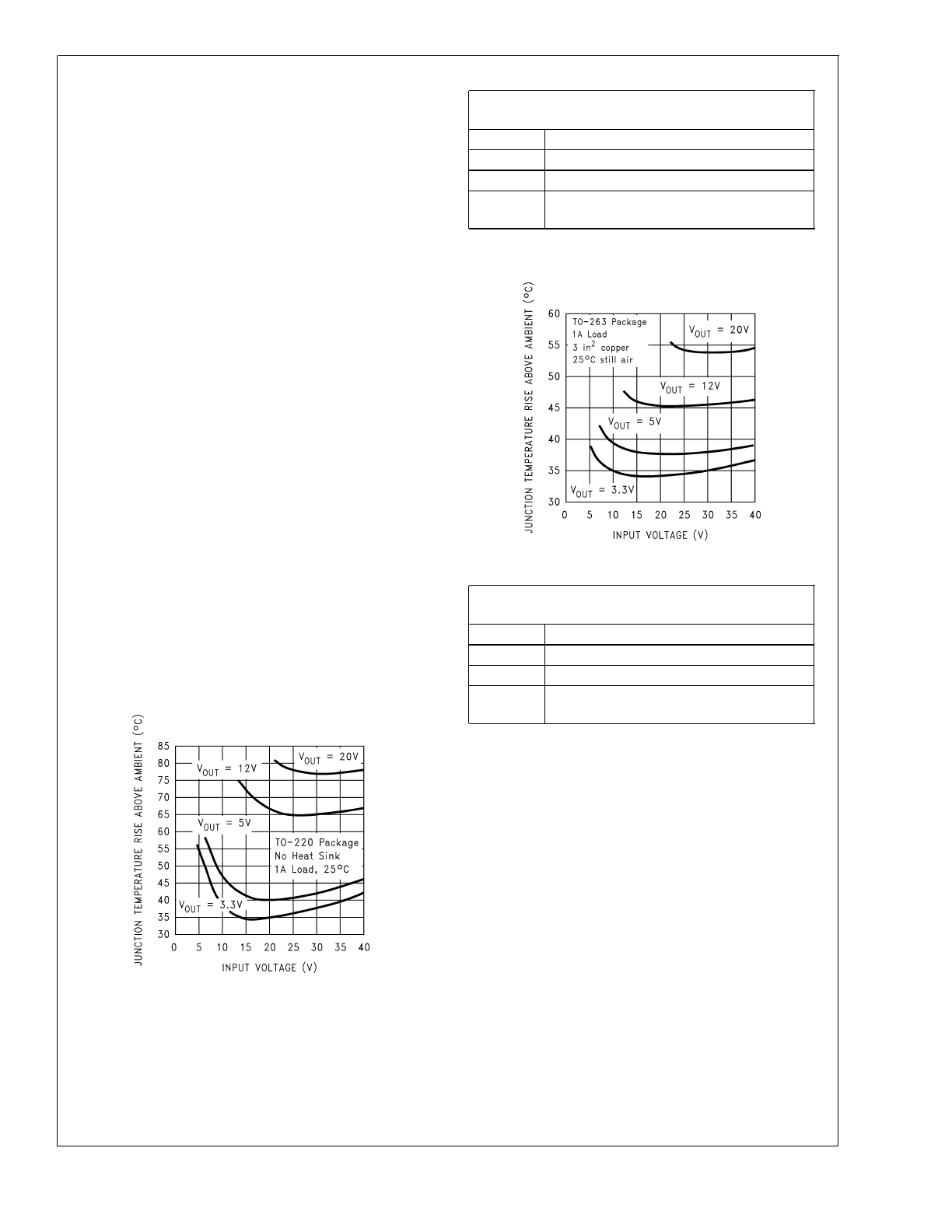
Application Information
(Continued)
These magnetic lines of flux will induce a voltage into any
wire or PC board copper trace that comes within the induc-
tor’s magnetic field. The strength of the magnetic field, the
orientation and location of the PC copper trace to the mag-
netic field, and the distance between the copper trace and
the inductor, determine the amount of voltage generated in
the copper trace. Another way of looking at this inductive
coupling is to consider the PC board copper trace as one
turn of a transformer (secondary) with the inductor winding
as the primary. Many millivolts can be generated in a copper
trace located near an open core inductor which can cause
stability problems or high output ripple voltage problems.
If unstable operation is seen, and an open core inductor is
used, it’s possible that the location of the inductor with re-
spect to other PC traces may be the problem. To determine
if this is the problem, temporarily raise the inductor away
from the board by several inches and then check circuit op-
eration. If the circuit now operates correctly, then the mag-
netic flux from the open core inductor is causing the problem.
Substituting a closed core inductor such as a torroid or
E-core will correct the problem, or re-arranging the PC layout
may be necessary. Magnetic flux cutting the IC device
ground trace, feedback trace, or the positive or negative
traces of the output capacitor should be minimized.
Sometimes, locating a trace directly beneath a bobbin in-
ductor will provide good results, provided it is exactly in the
center of the inductor (because the induced voltages cancel
themselves out), but if it is off center one direction or the
other, then problems could arise. If flux problems are
present, even the direction of the inductor winding can make
a difference in some circuits.
This discussion on open core inductors is not to frighten the
user, but to alert the user on what kind of problems to watch
out for when using them. Open core bobbin or “stick” induc-
tors are an inexpensive, simple way of making a compact ef-
ficient inductor, and they are used by the millions in many dif-
ferent applications.
THERMAL CONSIDERATIONS
The LM2598 is available in two packages, a 7-pin TO-220
(T) and a 7-pin surface mount TO-263 (S).
The TO-220 package can be used without a heat sink for
ambient temperatures up to approximately 50˚C (depending
on the output voltage and load current). The curves in
Figure
21
show the LM2598T junction temperature rises above am-
bient temperature for different input and output voltages. The
data for these curves was taken with the LM2598T (TO-220
package) operating as a switching regulator in an ambient
temperature of 25˚C (still air). These temperature rise num-
bers are all approximate and there are many factors that can
affect these temperatures. Higher ambient temperatures re-
quire some heat sinking, either to the PC board or a small
external heat sink.
The TO-263 surface mount package tab is designed to be
soldered to the copper on a printed circuit board. The copper
and the board are the heat sink for this package and the
other heat producing components, such as the catch diode
and inductor. The PC board copper area that the package is
soldered to should be at least 0.4 in
2
, and ideally should
have 2 or more square inches of 2 oz. (0.0028) in) copper.
DS012593-38
Circuit Data for Temperature Rise Curve TO-220
Package (T)
Capacitors
Through hole electrolytic
Inductor
Through hole, Schott, 68 µH
Diode
Through hole, 3A 40V, Schottky
PC board
3 square inches single sided 2 oz. copper
(0.0028")
FIGURE 21. Junction Temperature Rise, TO-220
DS012593-39
Circuit Data for Temperature Rise Curve TO-263
Package (S)
Capacitors
Surface mount tantalum, molded “D” size
Inductor
Surface mount, Schott, 68 µH
Diode
Surface mount, 3A 40V, Schottky
PC board
3 square inches single sided 2 oz. copper
(0.0028")
FIGURE 22. Junction Temperature Rise, TO-263
LM2598
www.national.com
25
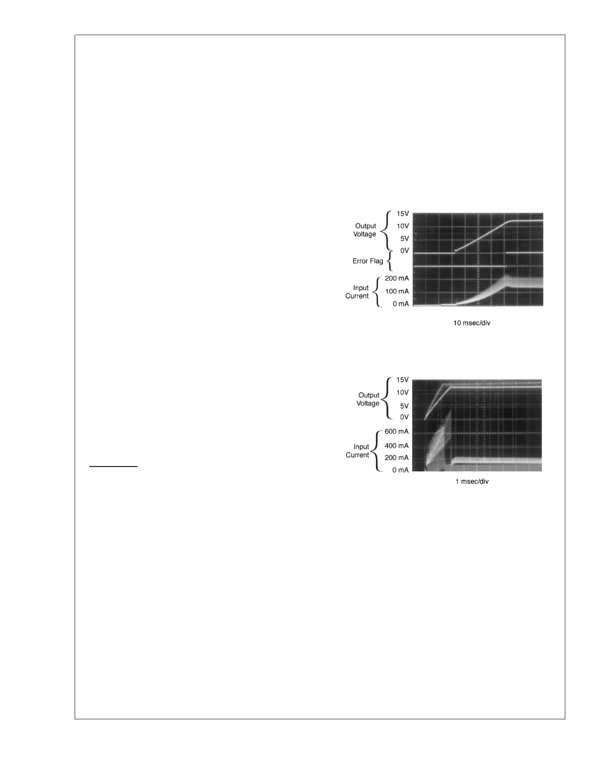
Application Information
(Continued)
Additional copper area improves the thermal characteristics,
but with copper areas greater than approximately 3 in
2
, only
small improvements in heat dissipation are realized. If fur-
ther thermal improvements are needed, double sided or mul-
tilayer PC-board with large copper areas are recommended.
The curves shown in
Figure 22
show the LM2598S (TO-263
package) junction temperature rise above ambient tempera-
ture with a 1A load for various input and output voltages. This
data was taken with the circuit operating as a buck switching
regulator with all components mounted on a PC board to
simulate the junction temperature under actual operating
conditions. This curve can be used for a quick check for the
approximate junction temperature for various conditions, but
be aware that there are many factors that can affect the junc-
tion temperature.
For the best thermal performance, wide copper traces and
generous amounts of printed circuit board copper should be
used in the board layout. (One exception to this is the output
(switch) pin, which should not have large areas of copper.)
Large areas of copper provide the best transfer of heat
(lower thermal resistance) to the surrounding air, and moving
air lowers the thermal resistance even further.
Package thermal resistance and junction temperature rise
numbers are all approximate, and there are many factors
that will affect these numbers. Some of these factors include
board size, shape, thickness, position, location, and even
board temperature. Other factors are, trace width, total
printed circuit copper area, copper thickness, single- or
double-sided, multilayer board and the amount of solder on
the board. The effectiveness of the PC board to dissipate
heat also depends on the size, quantity and spacing of other
components on the board, as well as whether the surround-
ing air is still or moving. Furthermore, some of these compo-
nents such as the catch diode will add heat to the PC board
and the heat can vary as the input voltage changes. For the
inductor, depending on the physical size, type of core mate-
rial and the DC resistance, it could either act as a heat sink
taking heat away from the board, or it could add heat to the
board.
SHUTDOWN /SOFT-START
The circuit shown in
Figure 25
is a standard buck regulator
with 24V in, 12V out, 280 mA load, and using a 0.068 µF
Soft-start capacitor. The photo in
Figure 23
and
Figure 24
show the effects of Soft-start on the output voltage, the input
current, with, and without a Soft-start capacitor.
Figure 23
also shows the error flag output going high when the output
voltage reaches 95% of the nominal output voltage. The re-
duced input current required at startup is very evident when
comparing the two photos. The Soft-start feature reduces the
startup current from 1A down to 240 mA, and delays and
slows down the output voltage rise time.
This reduction in start up current is useful in situations where
the input power source is limited in the amount of current it
can deliver. In some applications Soft-start can be used to
replace undervoltage lockout or delayed startup functions.
If a very slow output voltage ramp is desired, the Soft-start
capacitor can be made much larger. Many seconds or even
minutes are possible.
If only the shutdown feature is needed, the Soft-start capaci-
tor can be eliminated.
DS012593-40
FIGURE 23. Output Voltage, Input Current, Error Flag
Signal, at Start-Up, WITH Soft-start
DS012593-41
FIGURE 24. Output Voltage, Input Current, at Start-Up,
WITHOUT Soft-start
LM2598
www.national.com
26
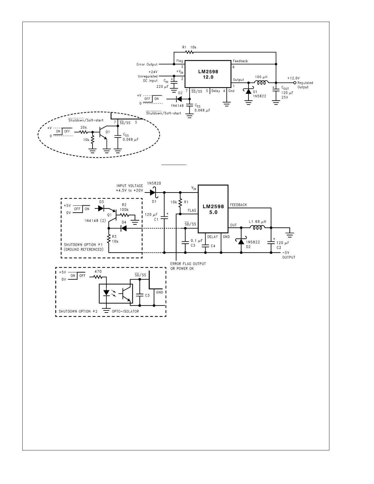
Application Information
(Continued)
lNVERTING REGULATOR
The circuit in
Figure 26
converts a positive input voltage to a
negative output voltage with a common ground. The circuit
operates by bootstrapping the regulators ground pin to the
negative output voltage, then grounding the feedback pin,
the regulator senses the inverted output voltage and regu-
lates it.
This example uses the LM2598-5 to generate a −5V output,
but other output voltages are possible by selecting other out-
put voltage versions, including the adjustable version. Since
this regulator topology can produce an output voltage that is
either greater than or less than the input voltage, the maxi-
mum output current greatly depends on both the input and
output voltage. The curve shown in
Figure 27
provides a
guide as to the amount of output load current possible for the
different input and output voltage conditions.
The maximum voltage appearing across the regulator is the
absolute sum of the input and output voltage, and this must
be limited to a maximum of 40V. In this example, when con-
verting +20V to −5V, the regulator would see 25V between
the input pin and ground pin. The LM2598 has a maximum
input voltage rating of 40V.
DS012593-42
FIGURE 25. Typical Circuit Using Shutdown /Soft-start and Error Flag Features
DS012593-43
FIGURE 26. Inverting −5V Regulator With Shutdown and Soft-start
LM2598
www.national.com
27
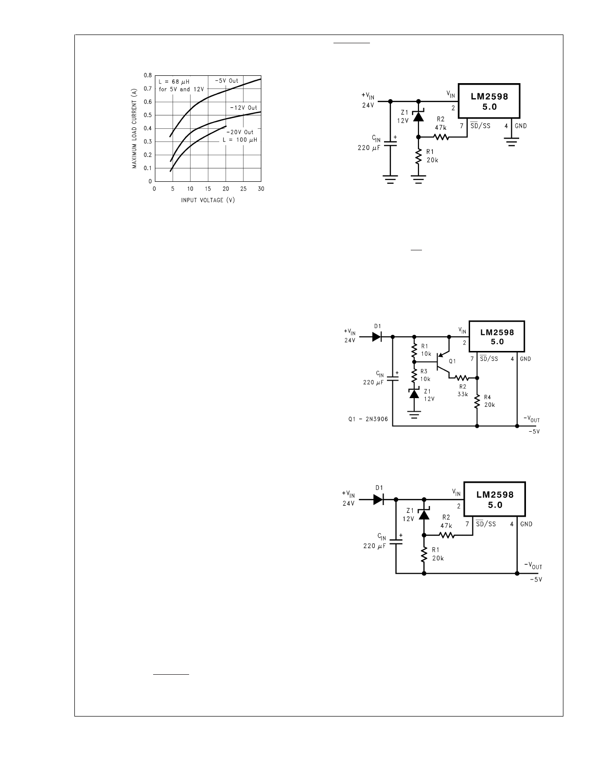
Application Information
(Continued)
An additional diode is required in this regulator configuration.
Diode D1 is used to isolate input voltage ripple or noise from
coupling through the C
IN
capacitor to the output, under light
or no load conditions. Also, this diode isolation changes the
topology to closely resemble a buck configuration thus pro-
viding good closed loop stability. A Schottky diode is recom-
mended for low input voltages, (because of its lower voltage
drop) but for higher input voltages, a 1N5400 diode could be
used.
Because of differences in the operation of the inverting regu-
lator, the standard design procedure is not used to select the
inductor value. In the majority of designs, a 68 µH, 1.5 Amp
inductor is the best choice. Capacitor selection can also be
narrowed down to just a few values. Using the values shown
in
Figure 26
will provide good results in the majority of invert-
ing designs.
This type of inverting regulator can require relatively large
amounts of input current when starting up, even with light
loads. Input currents as high as the LM2598 current limit (ap-
proximately 1.5A) are needed for 2 ms or more, until the out-
put reaches its nominal output voltage. The actual time de-
pends on the output voltage and the size of the output
capacitor. Input power sources that are current limited or
sources that can not deliver these currents without getting
loaded down, may not work correctly. Because of the rela-
tively high startup currents required by the inverting topology,
the Soft-start feature shown in
Figure 26
is recommended.
Also shown in
Figure 26
are several shutdown methods for
the inverting configuration. With the inverting configuration,
some level shifting is required, because the ground pin of the
regulator is no longer at ground, but is now at the negative
output voltage. The shutdown methods shown accept
ground referenced shutdown signals.
UNDERVOLTAGE LOCKOUT
Some applications require the regulator to remain off until
the input voltage reaches a predetermined voltage.
Figure
28
contains a undervoltage lockout circuit for a buck configu-
ration, while
Figure 29
and
Figure 30
are for the inverting
types (only the circuitry pertaining to the undervoltage lock-
out is shown).
Figure 28
uses a zener diode to establish the
threshold voltage when the switcher begins operating. When
the input voltage is less than the zener voltage, resistors R1
and R2 hold the Shutdown /Soft-start pin low, keeping the
regulator in the shutdown mode. As the input voltage ex-
ceeds the zener voltage, the zener conducts, pulling the
Shutdown /Soft-start pin high, allowing the regulator to begin
switching. The threshold voltage for the undervoltage lockout
feature is approximately 1.5V greater than the zener voltage.
Figure 29
and
Figure 30
apply the same feature to an invert-
ing circuit.
Figure 29
features a constant threshold voltage
for turn on and turn off (zener voltage plus approximately
one volt). Since the SD /SS pin has an internal 7V zener
clamp, R2 is needed to limit the current into this pin to ap-
proximately 1 mA when Q1 is on. If hysteresis is needed, the
circuit in
Figure 30
has a turn ON voltage which is different
than the turn OFF voltage. The amount of hysteresis is ap-
proximately equal to the value of the output voltage.
NEGATIVE VOLTAGE CHARGE PUMP
Occasionally a low current negative voltage is needed for bi-
asing parts of a circuit. A simple method of generating a
negative voltage using a charge pump technique and the
switching waveform present at the OUT pin, is shown in
Fig-
ure 31
. This unregulated negative voltage is approximately
equal to the positive input voltage (minus a few volts), and
can supply up to a 200 mA of output current. There is a re-
quirement however, that there be a minimum load of several
DS012593-44
FIGURE 27. Maximum Load Current for Inverting
Regulator Circuit
DS012593-45
FIGURE 28. Undervoltage Lockout for a Buck
Regulator
DS012593-47
FIGURE 29. Undervoltage Lockout Without
Hysteresis for an Inverting Regulator
DS012593-46
FIGURE 30. Undervoltage Lockout With
Hysteresis for an Inverting Regulator
LM2598
www.national.com
28
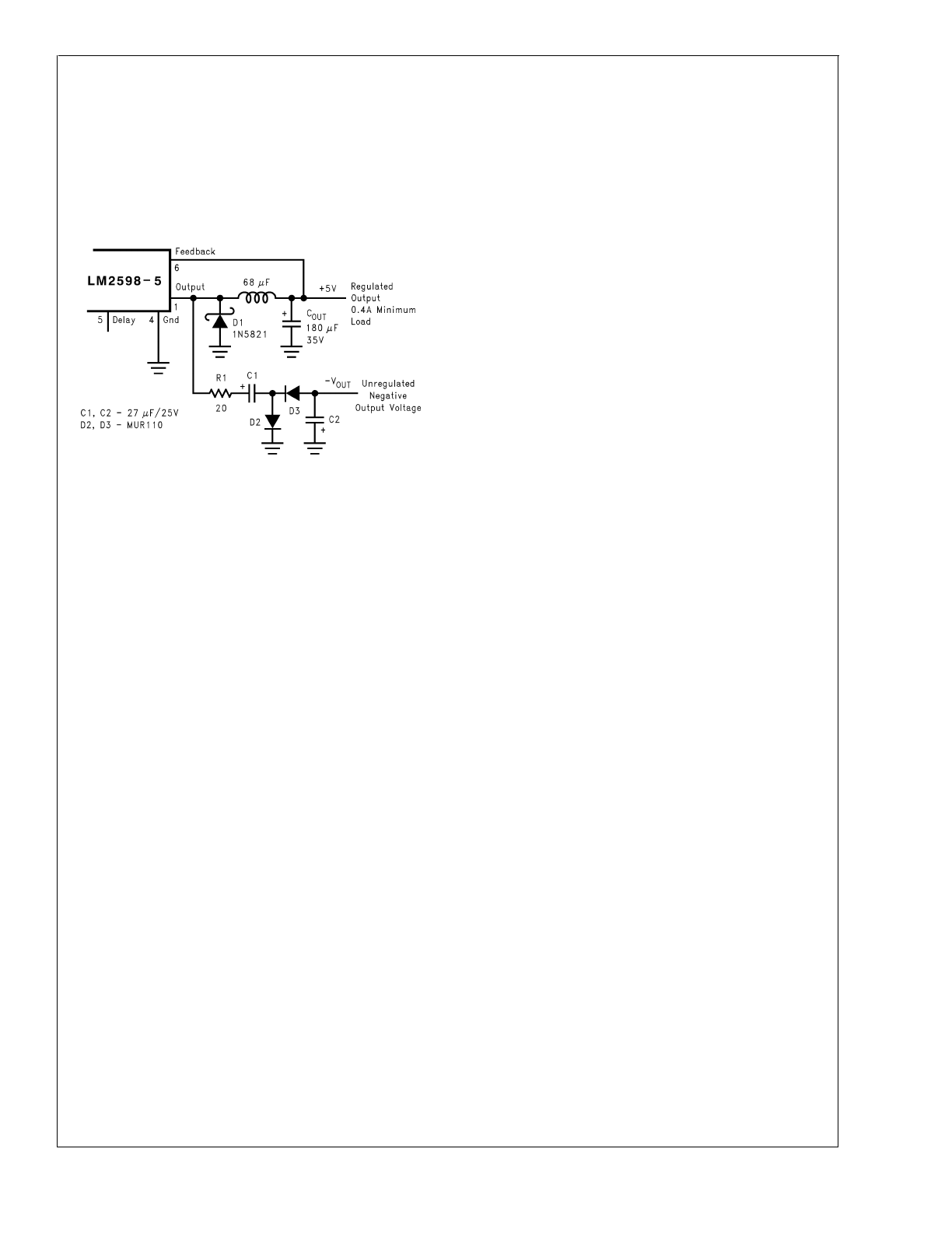
Application Information
(Continued)
hundred mA on the regulated positive output for the charge
pump to work correctly. Also, resistor R1 is required to limit
the charging current of C1 to some value less than the
LM2598 current limit (typically 1.5A).
This method of generating a negative output voltage without
an additional inductor can be used with other members of
the Simple Switcher Family, using either the buck or boost
topology.
DS012593-48
FIGURE 31. Charge Pump for Generating a
Low Current, Negative Output Voltage
LM2598
www.national.com
29
Application Information
(Continued)
TYPICAL THROUGH HOLE PC BOARD LAYOUT, FIXED OUTPUT (1X SIZE), DOUBLE SIDED, THROUGH HOLE
PLATED
DS012593-51
C
IN
— 150 µF/50V Aluminum Electrolytic, Panasonic “HFQ series”
R
PULL-UP
— 10 k
Ω
C
OUT
— 120 µF/25V Aluminum Electrolytic, Panasonic “HFQ series”
C
DELAY
— 0.1 µF
D1 — 3A, 40V Schottky Rectifier, 1N5822
C
SD/SS
— 0.1 µF
L1 — 68 µH, L30, Renco, Through hole
FIGURE 32. Fixed Output PC Board Layout
LM2598
www.national.com
30
Application Information
(Continued)
TYPICAL THROUGH HOLE PC BOARD LAYOUT, ADJUSTABLE OUTPUT (1X SIZE), DOUBLE SIDED,
THROUGH HOLE PLATED
DS012593-52
C
IN
— 150 µF/50V, Aluminum Electrolytic, Panasonic “HFQ series”
C
FF
— See
Figure 4.
C
OUT
— 120 µF/25V Aluminum Electrolytic, Panasonic “HFQ series”
R
FF
— See Application Information Section (C
FF
Section)
D1 — 3A, 40V Schottky Rectifier, 1N5822
R
PULL-UP
— 10 k
Ω
L1 — 68 µH, L30, Renco, Through hole
C
DELAY
— 0.1 µF
R1 — 1 k
Ω
, 1%
C
SD/SS
— 0.1 µF
R2 — Use formula in Design Procedure
FIGURE 33. Adjustable Output PC Board Layout
LM2598
www.national.com
31
Physical Dimensions
inches (millimeters) unless otherwise noted
7-Lead TO-220 (T)
Order Number LM2598T-3.3, LM2598T-5.0,
LM2598T-12 or LM2598T-ADJ
NS Package Number TA07B
LM2598
www.national.com
32
Physical Dimensions
inches (millimeters) unless otherwise noted (Continued)
LIFE SUPPORT POLICY
NATIONAL’S PRODUCTS ARE NOT AUTHORIZED FOR USE AS CRITICAL COMPONENTS IN LIFE SUPPORT
DEVICES OR SYSTEMS WITHOUT THE EXPRESS WRITTEN APPROVAL OF THE PRESIDENT AND GENERAL
COUNSEL OF NATIONAL SEMICONDUCTOR CORPORATION. As used herein:
1. Life support devices or systems are devices or
systems which, (a) are intended for surgical implant
into the body, or (b) support or sustain life, and
whose failure to perform when properly used in
accordance with instructions for use provided in the
labeling, can be reasonably expected to result in a
significant injury to the user.
2. A critical component is any component of a life
support device or system whose failure to perform
can be reasonably expected to cause the failure of
the life support device or system, or to affect its
safety or effectiveness.
National Semiconductor
Corporation
Americas
Tel: 1-800-272-9959
Fax: 1-800-737-7018
Email: support@nsc.com
National Semiconductor
Europe
Fax: +49 (0) 180-530 85 86
Email: europe.support@nsc.com
Deutsch Tel: +49 (0) 69 9508 6208
English
Tel: +44 (0) 870 24 0 2171
Français Tel: +33 (0) 1 41 91 8790
National Semiconductor
Asia Pacific Customer
Response Group
Tel: 65-2544466
Fax: 65-2504466
Email: ap.support@nsc.com
National Semiconductor
Japan Ltd.
Tel: 81-3-5639-7560
Fax: 81-3-5639-7507
www.national.com
7-Lead TO-263 Surface Mount Package (S)
Order Number LM2598S-3.3, LM2598S-5.0, LM2598S-12 or LM2598S-ADJ
NS Package Number TS7B
LM2598
SIMPLE
SWITCHER
Power
Converter
150
kHz
1A
Step-Down
V
oltage
Regulator
,
with
Features
National does not assume any responsibility for use of any circuitry described, no circuit patent licenses are implied and National reserves the right at any time without notice to change said circuitry and specifications.