
LM1575/LM2575/LM2575HV Series
SIMPLE SWITCHER
®
1A Step-Down Voltage Regulator
General Description
The LM2575 series of regulators are monolithic integrated
circuits that provide all the active functions for a step-down
(buck) switching regulator, capable of driving a 1A load with
excellent line and load regulation. These devices are avail-
able in fixed output voltages of 3.3V, 5V, 12V, 15V, and an
adjustable output version.
Requiring a minimum number of external components, these
regulators are simple to use and include internal frequency
compensation and a fixed-frequency oscillator.
The LM2575 series offers a high-efficiency replacement for
popular three-terminal linear regulators. It substantially re-
duces the size of the heat sink, and in many cases no heat
sink is required.
A standard series of inductors optimized for use with the
LM2575 are available from several different manufacturers.
This feature greatly simplifies the design of switch-mode
power supplies.
Other features include a guaranteed
±
4% tolerance on out-
put voltage within specified input voltages and output load
conditions, and
±
10% on the oscillator frequency. External
shutdown is included, featuring 50 µA (typical) standby cur-
rent. The output switch includes cycle-by-cycle current limit-
ing, as well as thermal shutdown for full protection under
fault conditions.
Features
n
3.3V, 5V, 12V, 15V, and adjustable output versions
n
Adjustable version output voltage range,
1.23V to 37V (57V for HV version)
±
4% max over
line and load conditions
n
Guaranteed 1A output current
n
Wide input voltage range, 40V up to 60V for HV version
n
Requires only 4 external components
n
52 kHz fixed frequency internal oscillator
n
TTL shutdown capability, low power standby mode
n
High efficiency
n
Uses readily available standard inductors
n
Thermal shutdown and current limit protection
n
P
+
Product Enhancement tested
Applications
n
Simple high-efficiency step-down (buck) regulator
n
Efficient pre-regualtor for linear regulators
n
On-card switching regulators
n
Positive to negative converter (Buck-Boost)
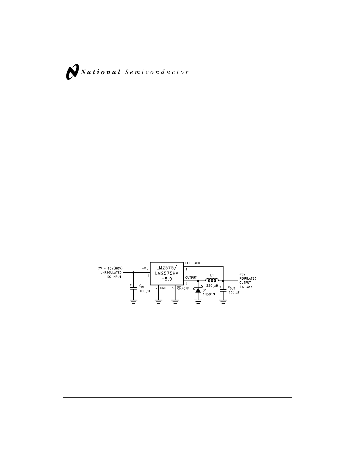
Typical Application
(Fixed Output Voltage Versions)
SIMPLE SWITCHER
®
is a registered trademark of National Semiconductor Corporation.
DS011475-1
Note: Pin numbers are for the TO-220 package.
May 1999
LM1575/LM2575/LM2575HV
Series
SIMPLE
SWITCHER
1A
Step-Down
V
oltage
Regulator
© 1999 National Semiconductor Corporation
DS011475
www.national.com
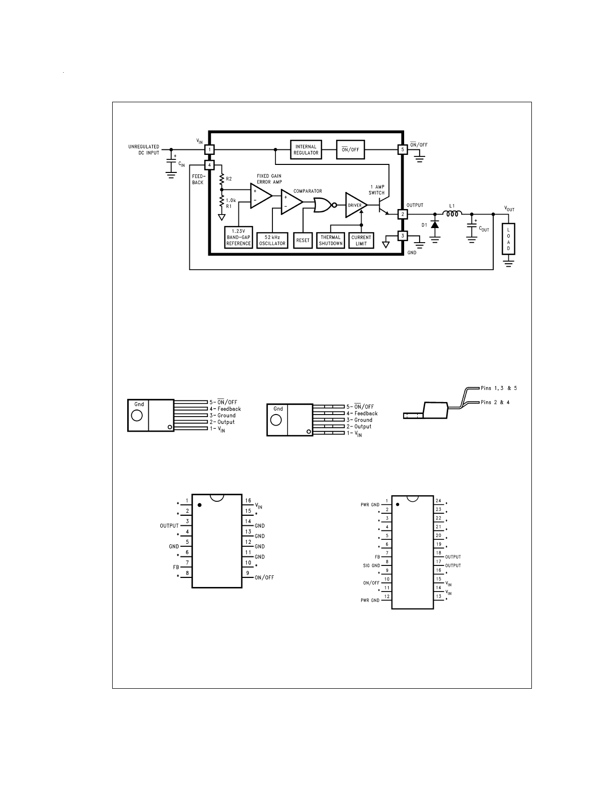
Block Diagram and Typical Application
Connection Diagrams
(XX indicates output voltage option. See Ordering Information table for complete part
number.)
DS011475-2
3.3V, R2 = 1.7k
5V, R2 = 3.1k
12V, R2 = 8.84k
15V, R2 = 11.3k
For ADJ. Version
R1 = Open, R2 = 0
Ω
Note: Pin numbers are for the TO-220 package.
FIGURE 1.
Straight Leads
5–Lead TO-22 (T)
DS011475-22
Top View
LM2575T-XX or LM2575HVT-XX
See NS Package Number T05A
Bent, Staggered Leads
5-Lead TO-220 (T)
DS011475-23
Top View
DS011475-24
Side View
LM2575T-XX Flow LB03 or
LM2575HVT-XX Flow LB03
See NS Package Number T05D
16–Lead DIP (N or J)
DS011475-25
*No Internal Connection
Top View
LM2575N-XX or LM2575HVN-XX
See NS Package Number N16A
LM1575J-XX-QML
See NS Package Number J16A
24-Lead Surface Mount (M)
DS011475-26
*No Internal Connection
Top View
LM2575M-XX or LM2575HVM-XX
See NS Package Number M24B
www.national.com
2
Connection Diagrams
(XX indicates output voltage option. See Ordering Information table for complete part
number.) (Continued)
Ordering Information
Package
NSC
Standard
High
Temperature
Type
Package
Voltage Rating
Voltage Rating
Range
Number
(40V)
(60V)
5-Lead TO-220
T05A
LM2575T-3.3
LM2575HVT-3.3
Straight Leads
LM2575T-5.0
LM2575HVT-5.0
LM2575T-12
LM2575HVT-12
LM2575T-15
LM2575HVT-15
LM2575T-ADJ
LM2575HVT-ADJ
5-Lead TO-220
T05D
LM2575T-3.3 Flow LB03
LM2575HVT-3.3 Flow LB03
Bent and
LM2575T-5.0 Flow LB03
LM2575HVT-5.0 Flow LB03
Staggered Leads
LM2575T-12 Flow LB03
LM2575HVT-12 Flow LB03
LM2575T-15 Flow LB03
LM2575HVT-15 Flow LB03
LM2575T-ADJ Flow LB03
LM2575HVT-ADJ Flow LB03
16-Pin Molded
N16A
LM2575N-5.0
LM2575HVN-5.0
−40˚C
≤
T
J
≤
+125˚C
DIP
LM2575N-12
LM2575HVN-12
LM2575N-15
LM2575HVN-15
LM2575N-ADJ
LM2575HVN-ADJ
24-Pin
M24B
LM2575M-5.0
LM2575HVM-5.0
Surface Mount
LM2575M-12
LM2575HVM-12
LM2575M-15
LM2575HVM-15
LM2575M-ADJ
LM2575HVM-ADJ
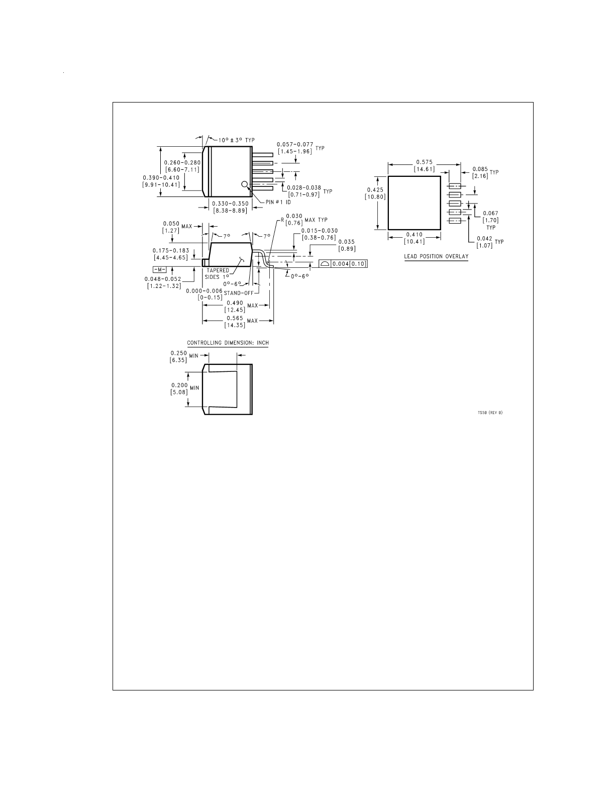
5-Lead TO-236
TS5B
LM2575S-3.3
LM2575HVS-3.3
Surface Mount
LM2575S-5.0
LM2575HVS-5.0
LM2575S-12
LM2575HVS-12
LM2575S-15
LM2575HVS-15
LM2575S-ADJ
LM2575HVS-ADJ
16-Pin Ceramic
J16A
LM1575J-3.3-QML
DIP
LM1575J-5.0-QML
LM1575J-12-QML
−55˚C
≤
T
J
≤
+150˚C
LM1575J-15-QML
LM1575J-ADJ-QML
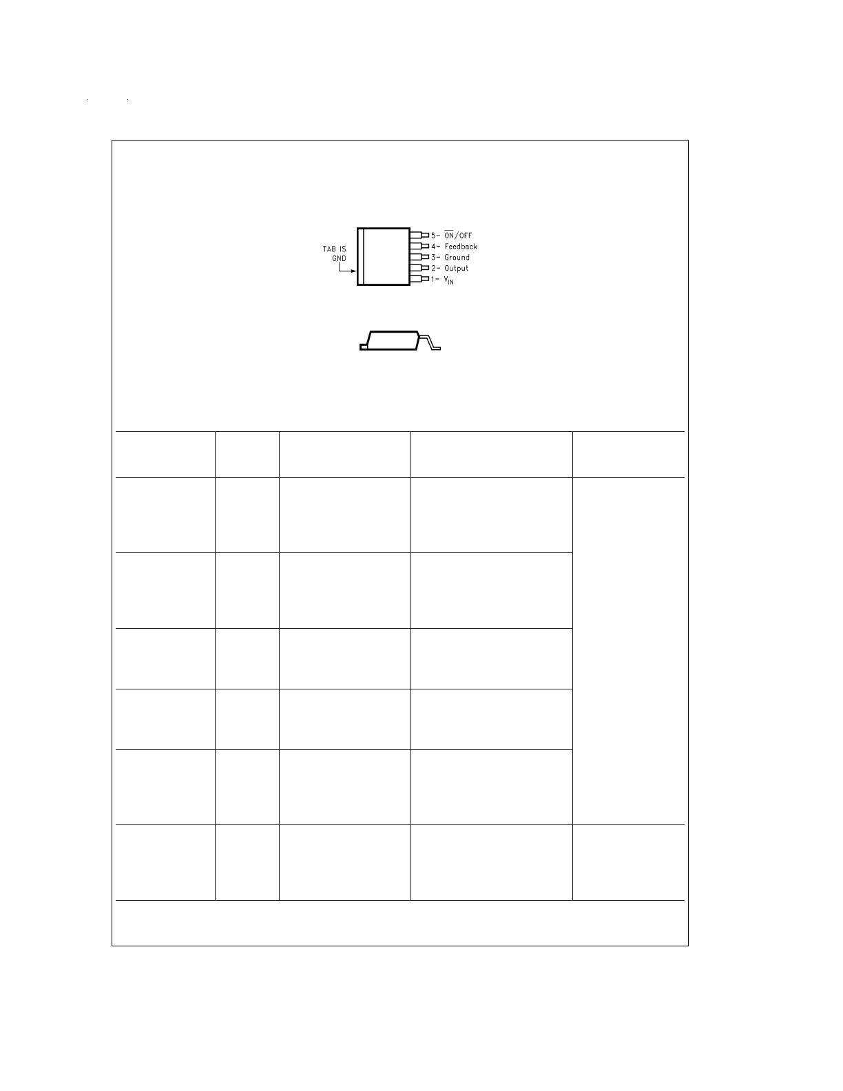
TO-263(S)
5-Lead Surface-Mount Package
DS011475-29
Top View
DS011475-30
Side View
LM2575S-XX or LM2575HVS-XX
See NS Package Number TS5B
www.national.com
3
Absolute Maximum Ratings
(Note 1)
If Military/Aerospace specified devices are required,
please contact the National Semiconductor Sales Office/
Distributors for availability and specifications.
Maximum Supply Voltage
LM1575/LM2575
45V
LM2575HV
63V
ON /OFF Pin Input Voltage
−0.3V
≤
V
≤
+V
IN
Output Voltage to Ground
(Steady State)
−1V
Power Dissipation
Internally Limited
Storage Temperature Range
−65˚C to +150˚C
Maximum Junction Temperature
150˚C
Minimum ESD Rating
(C = 100 pF, R = 1.5 k
Ω
)
2 kV
Lead Temperature
(Soldering, 10 sec.)
260˚C
Operating Ratings
Temperature Range
LM1575
−55˚C
≤
T
J
≤
+150˚C
LM2575/LM2575HV
−40˚C
≤
T
J
≤
+125˚C
Supply Voltage
LM1575/LM2575
40V
LM2575HV
60V
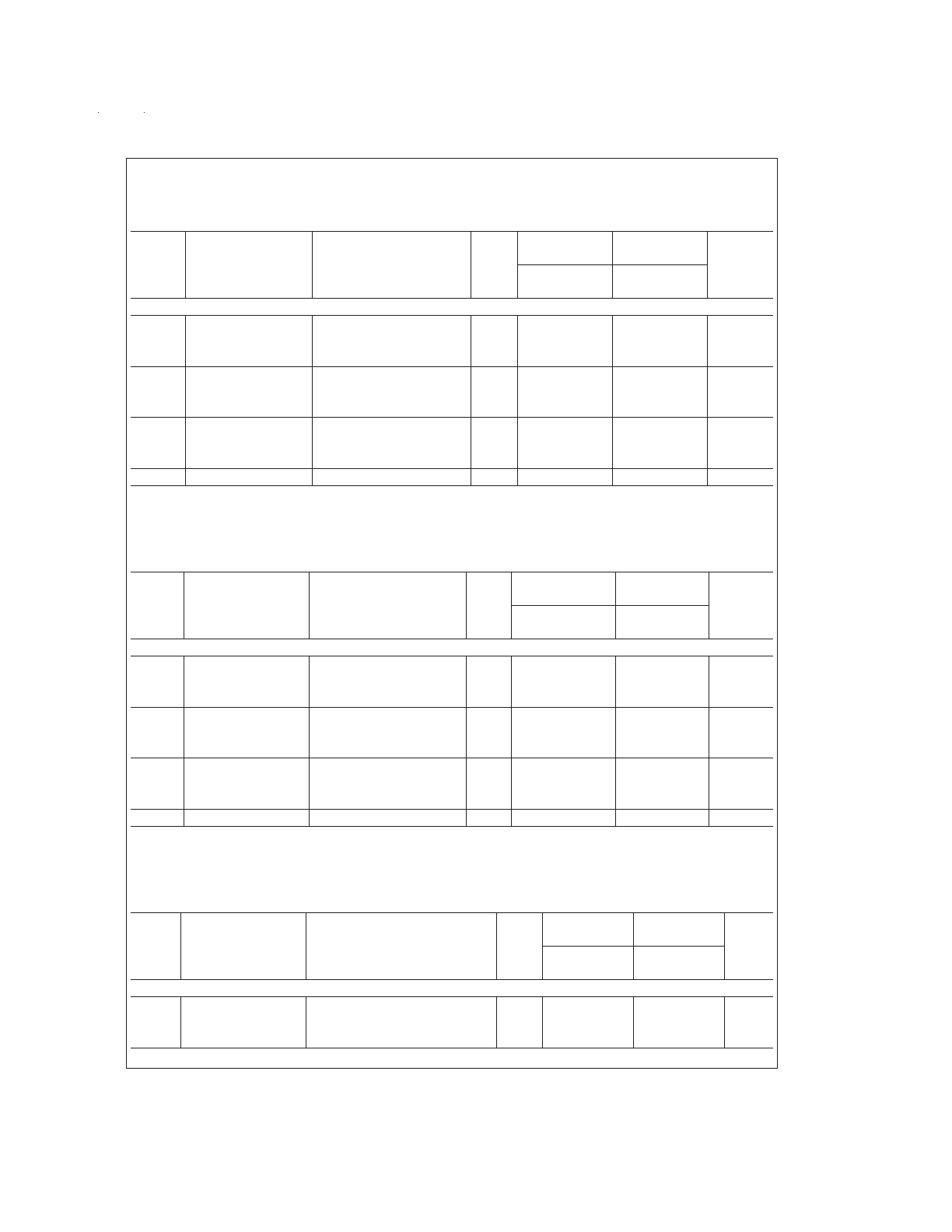
LM1575-3.3, LM2575-3.3, LM2575HV-3.3
Electrical Characteristics
Specifications with standard type face are for T
J
= 25˚C, and those with boldface type apply over full Operating Tempera-
ture Range .
Symbol
Parameter
Conditions
Typ
LM1575-3.3
LM2575-3.3
Units
(Limits)
LM2575HV-3.3
Limit
Limit
(Note 2)
(Note 3)
SYSTEM PARAMETERS (Note 4) Test Circuit
Figure 2
V
OUT
Output Voltage
V
IN
= 12V, I
LOAD
= 0.2A
3.3
V
Circuit of
Figure 2
3.267
3.234
V(Min)
3.333
3.366
V(Max)
V
OUT
Output Voltage
4.75V
≤
V
IN
≤
40V, 0.2A
≤
I
LOAD
≤
1A
3.3
V
LM1575/LM2575
Circuit of
Figure 2
3.200/3.168
3.168/3.135
V(Min)
3.400/3.432
3.432/3.465
V(Max)
V
OUT
Output Voltage
4.75V
≤
V
IN
≤
60V, 0.2A
≤
I
LOAD
≤
1A
3.3
V
LM2575HV
Circuit of
Figure 2
3.200/3.168
3.168/3.135
V(Min)
3.416/3.450
3.450/3.482
V(Max)
η
Efficiency
V
IN
= 12V, I
LOAD
= 1A
75
%
LM1575-5.0, LM2575-5.0, LM2575HV-5.0
Electrical Characteristics
Specifications with standard type face are for T
J
= 25˚C, and those with boldface type apply over full Operating Tempera-
ture Range.
Symbol
Parameter
Conditions
Typ
LM1575-5.0
LM2575-5.0
Units
(Limits)
LM2575HV-5.0
Limit
Limit
(Note 2)
(Note 3)
SYSTEM PARAMETERS (Note 4) Test Circuit
Figure 2
V
OUT
Output Voltage
V
IN
= 12V, I
LOAD
= 0.2A
5.0
V
Circuit of
Figure 2
4.950
4.900
V(Min)
5.050
5.100
V(Max)
V
OUT
Output Voltage
0.2A
≤
I
LOAD
≤
1A,
5.0
V
LM1575/LM2575
8V
≤
V
IN
≤
40V
4.850/4.800
4.800/4.750
V(Min)
Circuit of
Figure 2
5.150/5.200
5.200/5.250
V(Max)
V
OUT
Output Voltage
0.2A
≤
I
LOAD
≤
1A,
5.0
V
LM2575HV
8V
≤
V
IN
≤
60V
4.850/4.800
4.800/4.750
V(Min)
Circuit of
Figure 2
5.175/5.225
5.225/5.275
V(Max)
η
Efficiency
V
IN
= 12V, I
LOAD
= 1A
77
%
www.national.com
4
LM1575-12, LM2575-12, LM2575HV-12
Electrical Characteristics
Specifications with standard type face are for T
J
= 25˚C, and those with boldface type apply over full Operating Tempera-
ture Range .
Symbol
Parameter
Conditions
Typ
LM1575-12
LM2575-12
Units
(Limits)
LM2575HV-12
Limit
Limit
(Note 2)
(Note 3)
SYSTEM PARAMETERS (Note 4) Test Circuit
Figure 2
V
OUT
Output Voltage
V
IN
= 25V, I
LOAD
= 0.2A
12
V
Circuit of
Figure 2
11.88
11.76
V(Min)
12.12
12.24
V(Max)
V
OUT
Output Voltage
0.2A
≤
I
LOAD
≤
1A,
12
V
LM1575/LM2575
15V
≤
V
IN
≤
40V
11.64/11.52
11.52/11.40
V(Min)
Circuit of
Figure 2
12.36/12.48
12.48/12.60
V(Max)
V
OUT
Output Voltage
0.2A
≤
I
LOAD
≤
1A,
12
V
LM2575HV
15V
≤
V
IN
≤
60V
11.64/11.52
11.52/11.40
V(Min)
Circuit of
Figure 2
12.42/12.54
12.54/12.66
V(Max)
η
Efficiency
V
IN
= 15V, I
LOAD
= 1A
88
%
LM1575-15, LM2575-15, LM2575HV-15
Electrical Characteristics
Specifications with standard type face are for T
J
= 25˚C, and those with boldface type apply over full Operating Tempera-
ture Range .
Symbol
Parameter
Conditions
Typ
LM1575-15
LM2575-15
Units
(Limits)
LM2575HV-15
Limit
Limit
(Note 2)
(Note 3)
SYSTEM PARAMETERS (Note 4) Test Circuit
Figure 2
V
OUT
Output Voltage
V
IN
= 30V, I
LOAD
= 0.2A
15
V
Circuit of
Figure 2
14.85
14.70
V(Min)
15.15
15.30
V(Max)
V
OUT
Output Voltage
0.2A
≤
I
LOAD
≤
1A,
15
V
LM1575/LM2575
18V
≤
V
IN
≤
40V
14.55/14.40
14.40/14.25
V(Min)
Circuit of
Figure 2
15.45/15.60
15.60/15.75
V(Max)
V
OUT
Output Voltage
0.2A
≤
I
LOAD
≤
1A,
15
V
LM2575HV
18V
≤
V
IN
≤
60V
14.55/14.40
14.40/14.25
V(Min)
Circuit of
Figure 2
15.525/15.675
15.68/15.83
V(Max)
η
Efficiency
V
IN
= 18V, I
LOAD
= 1A
88
%
LM1575-ADJ, LM2575-ADJ, LM2575HV-ADJ
Electrical Characteristics
Specifications with standard type face are for T
J
= 25˚C, and those with boldface type apply over full Operating Temperature
Range.
Symbol
Parameter
Conditions
Typ
LM1575-ADJ
LM2575-ADJ
Units
(Limits)
LM2575HV-ADJ
Limit
Limit
(Note 2)
(Note 3)
SYSTEM PARAMETERS (Note 4) Test Circuit
Figure 2
V
OUT
Feedback Voltage
V
IN
= 12V, I
LOAD
= 0.2A
1.230
V
V
OUT
= 5V
1.217
1.217
V(Min)
Circuit of
Figure 2
1.243
1.243
V(Max)
www.national.com
5
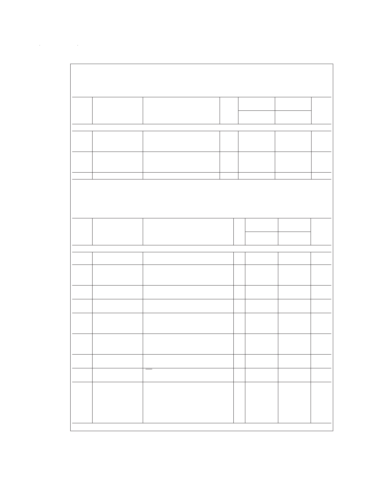
LM1575-ADJ, LM2575-ADJ, LM2575HV-ADJ
Electrical Characteristics
(Continued)
Specifications with standard type face are for T
J
= 25˚C, and those with boldface type apply over full Operating Temperature
Range.
Symbol
Parameter
Conditions
Typ
LM1575-ADJ
LM2575-ADJ
Units
(Limits)
LM2575HV-ADJ
Limit
Limit
(Note 2)
(Note 3)
SYSTEM PARAMETERS (Note 4) Test Circuit
Figure 2
V
OUT
Feedback Voltage
0.2A
≤
I
LOAD
≤
1A,
1.230
V
LM1575/LM2575
8V
≤
V
IN
≤
40V
1.205/1.193
1.193/1.180
V(Min)
V
OUT
= 5V, Circuit of
Figure 2
1.255/1.267
1.267/1.280
V(Max)
V
OUT
Feedback Voltage
0.2A
≤
I
LOAD
≤
1A,
1.230
V
LM2575HV
8V
≤
V
IN
≤
60V
1.205/1.193
1.193/1.180
V(Min)
V
OUT
= 5V, Circuit of
Figure 2
1.261/1.273
1.273/1.286
V(Max)
η
Efficiency
V
IN
= 12V, I
LOAD
= 1A, V
OUT
= 5V
77
%
All Output Voltage Versions
Electrical Characteristics
Specifications with standard type face are for T
J
= 25˚C, and those with boldface type apply over full Operating Temperature
Range. Unless otherwise specified, V
IN
= 12V for the 3.3V, 5V, and Adjustable version, V
IN
= 25V for the 12V version, and V
IN
= 30V for the 15V version. I
LOAD
= 200 mA.
Symbol
Parameter
Conditions
Typ
LM1575-XX
LM2575-XX
Units
(Limits)
LM2575HV-XX
Limit
Limit
(Note 2)
(Note 3)
DEVICE PARAMETERS
I
b
Feedback Bias
Current
V
OUT
= 5V (Adjustable Version Only)
50
100/500
100/500
nA
f
O
Oscillator Frequency
(Note 13)
52
kHz
47/43
47/42
kHz(Min)
58/62
58/63
kHz(Max)
V
SAT
Saturation Voltage
I
OUT
= 1A (Note 5)
0.9
V
1.2/1.4
1.2/1.4
V(Max)
DC
Max Duty Cycle (ON)
(Note 6)
98
%
93
93
%(Min)
I
CL
Current Limit
Peak Current (Notes 5, 13)
2.2
A
1.7/1.3
1.7/1.3
A(Min)
3.0/3.2
3.0/3.2
A(Max)
I
L
Output Leakage
(Notes 7, 8)
Output = 0V
2
2
mA(Max)
Current
Output = −1V
7.5
mA
Output = −1V
30
30
mA(Max)
I
Q
Quiescent Current
(Note 7)
5
mA
10/12
10
mA(Max)
I
STBY
Standby Quiescent
ON /OFF Pin = 5V (OFF)
50
µA
Current
200/500
200
µA(Max)
θ
JA
Thermal Resistance
T Package, Junction to Ambient (Note 9)
65
θ
JA
T Package, Junction to Ambient (Note 10)
45
˚C/W
θ
JC
T Package, Junction to Case
2
θ
JA
N Package, Junction to Ambient (Note 11)
85
θ
JA
M Package, Junction to Ambient (Note 11)
100
θ
JA
S Package, Junction to Ambient (Note 12)
37
www.national.com
6
All Output Voltage Versions
Electrical Characteristics
(Continued)
Specifications with standard type face are for T
J
= 25˚C, and those with boldface type apply over full Operating Temperature
Range. Unless otherwise specified, V
IN
= 12V for the 3.3V, 5V, and Adjustable version, V
IN
= 25V for the 12V version, and V
IN
= 30V for the 15V version. I
LOAD
= 200 mA.
Symbol
Parameter
Conditions
Typ
LM1575-XX
LM2575-XX
Units
(Limits)
LM2575HV-XX
Limit
Limit
(Note 2)
(Note 3)
ON /OFF CONTROL Test Circuit
Figure 2
V
IH
ON /OFF Pin Logic
V
OUT
= 0V
1.4
2.2/2.4
2.2/2.4
V(Min)
V
IL
Input Level
V
OUT
= Nominal Output Voltage
1.2
1.0/0.8
1.0/0.8
V(Max)
I
IH
ON /OFF Pin Input
ON /OFF Pin = 5V (OFF)
12
µA
Current
30
30
µA(Max)
I
IL
ON /OFF Pin = 0V (ON)
0
µA
10
10
µA(Max)
Note 1: Absolute Maximum Ratings indicate limits beyond which damage to the device may occur. Operating Ratings indicate conditions for which the device is in-
tended to be functional, but do not guarantee specific performance limits. For guaranteed specifications and test conditions, see the Electrical Characteristics.
Note 2: All limits guaranteed at room temperature (standard type face) and at temperature extremes (bold type face). All limts are used to calculate Average Out-
going Quality Level, and all are 100% production tested.
Note 3: All limits guaranteed at room temperature (standard type face) and at temperature extremes (bold type face). All room temperature limits are 100% pro-
duction tested. All limits at temperature extremes are guaranteed via correlation using standard Statistical Quality Control (SQC) methods.
Note 4: External components such as the catch diode, inductor, input and output capacitors can affect switching regulator system performance. When the LM1575/
LM2575 is used as shown in the
Figure 2
test circuit, system performance will be as shown in system parameters section of Electrical Characteristics.
Note 5: Output (pin 2) sourcing current. No diode, inductor or capacitor connected to output pin.
Note 6: Feedback (pin 4) removed from output and connected to 0V.
Note 7: Feedback (pin 4) removed from output and connected to +12V for the Adjustable, 3.3V, and 5V versions, and +25V for the 12V and 15V versions, to force
the output transistor OFF.
Note 8: V
IN
= 40V (60V for the high voltage version).
Note 9: Junction to ambient thermal resistance (no external heat sink) for the 5 lead TO-220 package mounted vertically, with
1
⁄
2
inch leads in a socket, or on a PC
board with minimum copper area.
Note 10: Junction to ambient thermal resistance (no external heat sink) for the 5 lead TO-220 package mounted vertically, with
1
⁄
2
inch leads soldered to a PC board
containing approximately 4 square inches of copper area surrounding the leads.
Note 11: Junction to ambient thermal resistance with approxmiately 1 square inch of pc board copper surrounding the leads. Additional copper area will lower thermal
resistance further. See thermal model in Switchers made Simple software.
Note 12: If the TO-263 package is used, the thermal resistance can be reduced by increasing the PC board copper area thermally connected to the package: Using
0.5 square inches of copper area,
θ
JA
is 50˚C/W; with 1 square inch of copper area,
θ
JA
is 37˚C/W; and with 1.6 or more square inches of copper area,
θ
JA
is 32˚C/W.
Note 13: The oscillator frequency reduces to approximately 18 kHz in the event of an output short or an overload which causes the regulated output voltage to drop
approximately 40% from the nominal output voltage. This self protection feature lowers the average power dissipation of the IC by lowering the minimum duty cycle
from 5% down to approximately 2%.
Note 14: Refer to RETS LM1575J for current revision of military RETS/SMD.
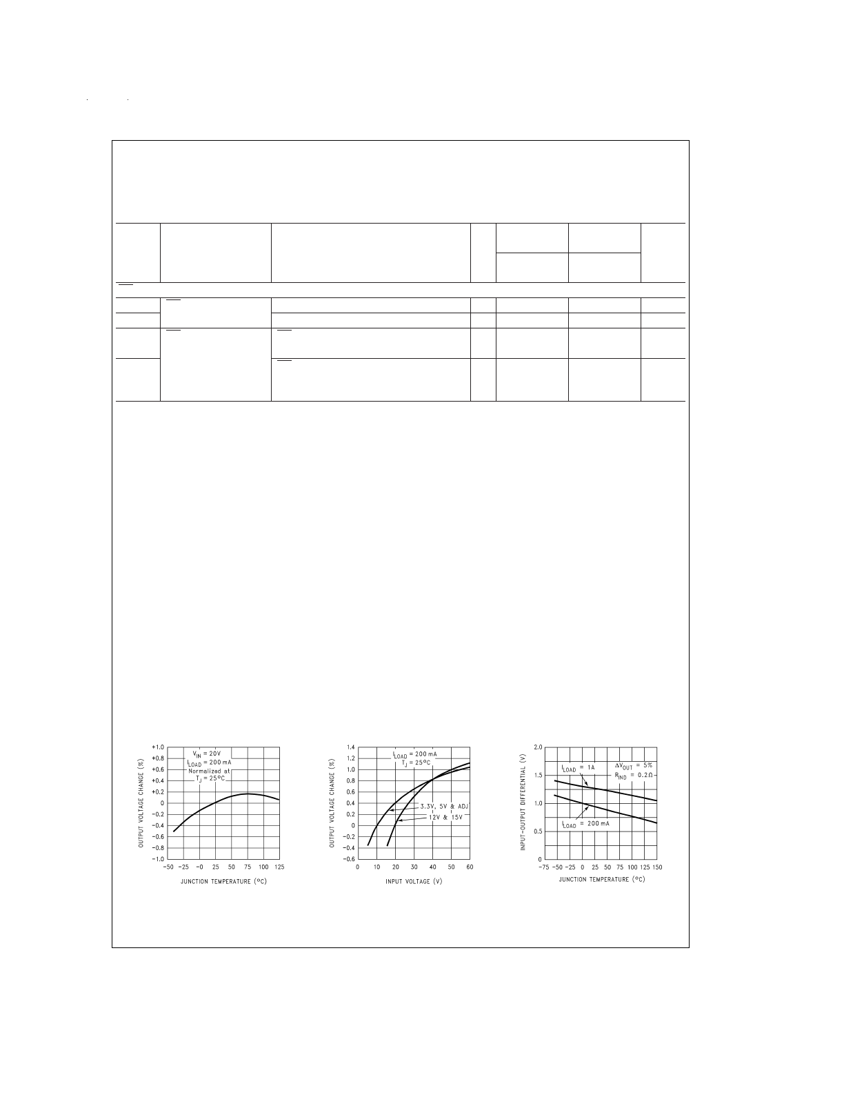
Typical Performance Characteristics
(Circuit of
Figure 2
)
Normalized Output Voltage
DS011475-32
Line Regulation
DS011475-33
Dropout Voltage
DS011475-34
www.national.com
7
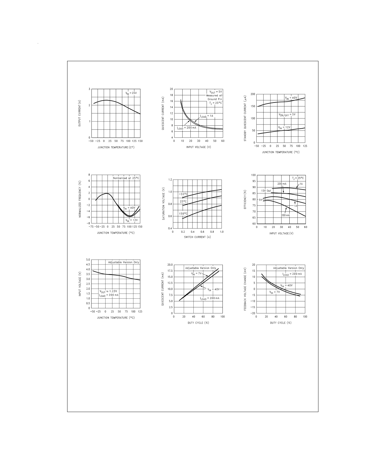
Typical Performance Characteristics
(Circuit of
Figure 2
) (Continued)
Current Limit
DS011475-35
Quiescent Current
DS011475-36
Standby
Quiescent Current
DS011475-37
Oscillator Frequency
DS011475-38
Switch Saturation
Voltage
DS011475-39
Efficiency
DS011475-40
Minimum Operating Voltage
DS011475-41
Quiescent Current
vs Duty Cycle
DS011475-42
Feedback Voltage
vs Duty Cycle
DS011475-43
www.national.com
8
Typical Performance Characteristics
(Circuit of
Figure 2
) (Continued)
Test Circuit and Layout Guidelines
As in any switching regulator, layout is very important. Rap-
idly switching currents associated with wiring inductance
generate voltage transients which can cause problems. For
minimal inductance and ground loops, the length of the leads
indicated by heavy lines should be kept as short as possible.
Single-point grounding (as indicated) or ground plane con-
struction should be used for best results. When using the Ad-
justable version, physically locate the programming resistors
near the regulator, to keep the sensitive feedback wiring
short.
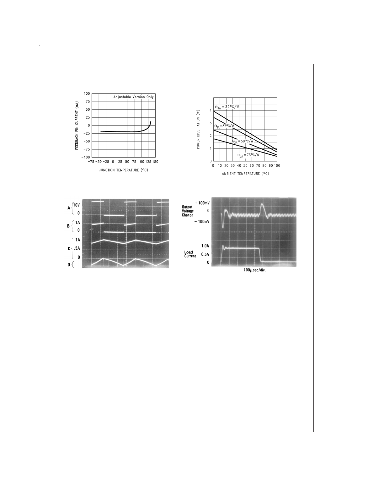
Feedback Pin Current
DS011475-5
Maximum Power Dissipation
(TO-263) (See (Note 12))
DS011475-28
Switching Waveforms
DS011475-6
V
OUT
= 5V
A: Output Pin Voltage, 10V/div
B: Output Pin Current, 1A/div
C: Inductor Current, 0.5A/div
D: Output Ripple Voltage, 20 mV/div,
AC-Coupled
Horizontal Time Base: 5 µs/div
Load Transient Response
DS011475-7
www.national.com
9
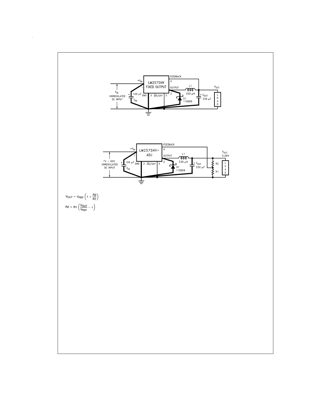
Test Circuit and Layout Guidelines
(Continued)
Fixed Output Voltage Versions
DS011475-8
C
IN
— 100 µF, 75V, Aluminum Electrolytic
C
OUT
— 330 µF, 25V, Aluminum Electrolytic
D1 — Schottky, 11DQ06
L1 — 330 µH, PE-52627 (for 5V in, 3.3V out, use 100 µH, PE-92108)
Adjustable Output Voltage Version
DS011475-9
where V
REF
= 1.23V, R1 between 1k and 5k.
R1 — 2k, 0.1%
R2 — 6.12k, 0.1%
Note: Pin numbers are for the TO-220 package.
FIGURE 2.
www.national.com
10
LM2575 Series Buck Regulator Design Procedure
PROCEDURE (Fixed Output Voltage Versions)
EXAMPLE (Fixed Output Voltage Versions)
Given:
V
OUT
= Regulated Output Voltage (3.3V, 5V, 12V, or 15V)
V
IN
(Max) = Maximum Input Voltage
I
LOAD
(Max) = Maximum Load Current
Given:
V
OUT
= 5V
V
IN
(Max) = 20V
I
LOAD
(Max) = 0.8A
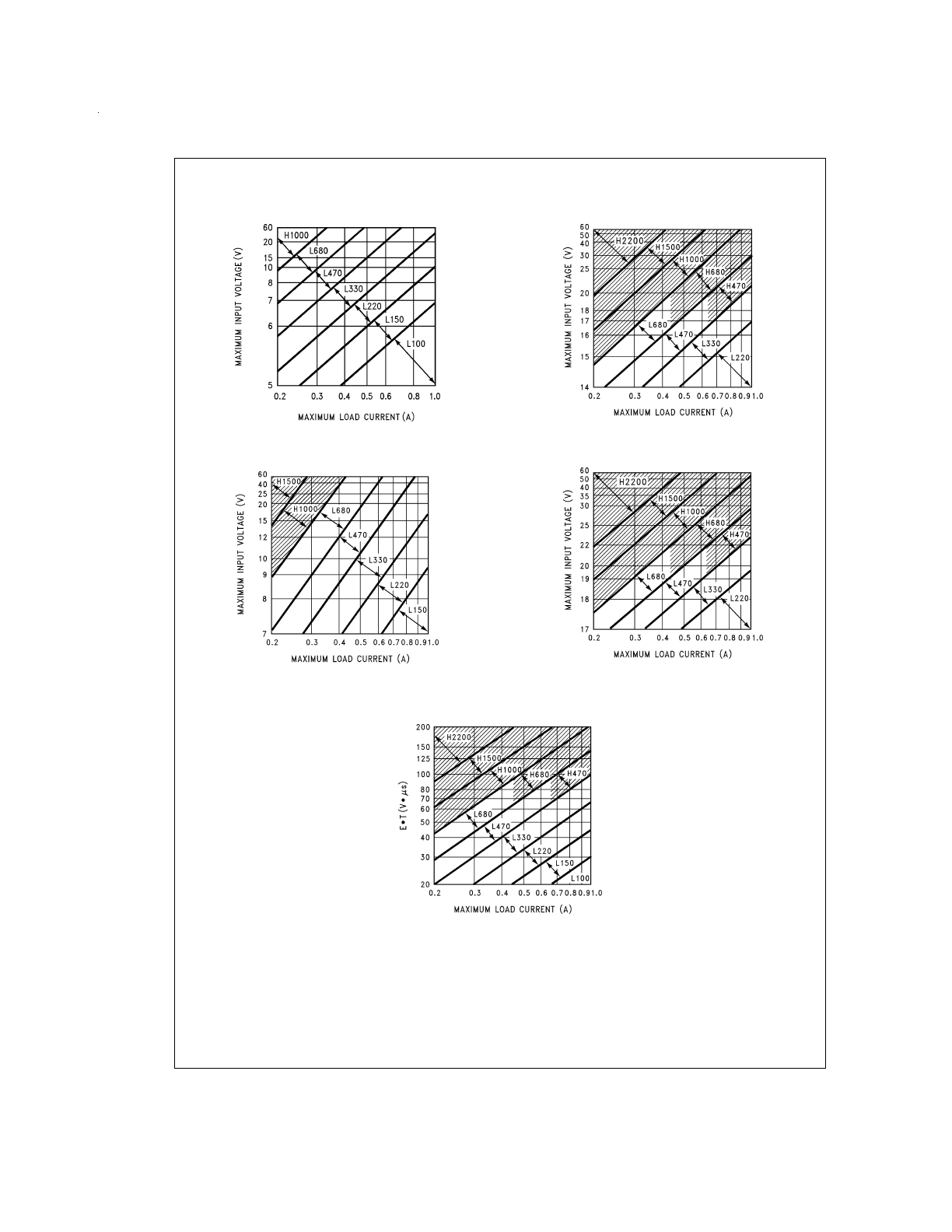
1. Inductor Selection (L1)
A. Select the correct Inductor value selection guide from
Fig-
ures 3, 4, 5, 6
(Output voltages of 3.3V, 5V, 12V or 15V re-
spectively). For other output voltages, see the design proce-
dure for the adjustable version.
B. From the inductor value selection guide, identify the in-
ductance region intersected by V
IN
(Max) and I
LOAD
(Max),
and note the inductor code for that region.
C. Identify the inductor value from the inductor code, and se-
lect an appropriate inductor from the table shown in
Figure 9
.
Part numbers are listed for three inductor manufacturers.
The inductor chosen must be rated for operation at the
LM2575 switching frequency (52 kHz) and for a current rat-
ing of 1.15 x I
LOAD
. For additional inductor information, see
the inductor section in the Application Hints section of this
data sheet.
1. Inductor Selection (L1)
A. Use the selection guide shown in
Figure 4
.
B. From the selection guide, the inductance area intersected
by the 20V line and 0.8A line is L330.
C. Inductor value required is 330 µH. From the table in
Fig-
ure 9
, choose AIE 415-0926, Pulse Engineering PE-52627,
or RL1952.
2. Output Capacitor Selection (C
OUT
)
A. The value of the output capacitor together with the induc-
tor defines the dominate pole-pair of the switching regulator
loop. For stable operation and an acceptable output ripple
voltage, (approximately 1% of the output voltage) a value be-
tween 100 µF and 470 µF is recommended.
B. The capacitor’s voltage rating should be at least 1.5 times
greater than the output voltage. For a 5V regulator, a rating
of at least 8V is appropriate, and a 10V or 15V rating is rec-
ommended.
Higher voltage electrolytic capacitors generally have lower
ESR numbers, and for this reasion it may be necessary to
select a capacitor rated for a higher voltage than would nor-
mally be needed.
2. Output Capacitor Selection (C
OUT
)
A. C
OUT
= 100 µF to 470 µF standard aluminum electrolytic.
B. Capacitor voltage rating = 20V.
3. Catch Diode Selection (D1)
A. The catch-diode current rating must be at least 1.2 times
greater than the maximum load current. Also, if the power
supply design must withstand a continuous output short, the
diode should have a current rating equal to the maximum
current limit of the LM2575. The most stressful condition for
this diode is an overload or shorted output condition.
B. The reverse voltage rating of the diode should be at least
1.25 times the maximum input voltage.
3. Catch Diode Selection (D1)
A. For this example, a 1A current rating is adequate.
B. Use a 30V 1N5818 or SR103 Schottky diode, or any of
the suggested fast-recovery diodes shown in
Figure 8
.
4. Input Capacitor (C
IN
)
An aluminum or tantalum electrolytic bypass capacitor lo-
cated close to the regulator is needed for stable operation.
4. Input Capacitor (C
IN
)
A 47 µF, 25V aluminum electrolytic capacitor located near
the input and ground pins provides sufficient bypassing.
www.national.com
11
(Continued)
INDUCTOR VALUE SELECTION GUIDES (For Continuous Mode Operation)
DS011475-10
FIGURE 3. LM2575(HV)-3.3
DS011475-11
FIGURE 4. LM2575(HV)-5.0
DS011475-12
FIGURE 5. LM2575(HV)-12
DS011475-13
FIGURE 6. LM2575(HV)-15
DS011475-14
FIGURE 7. LM2575(HV)-ADJ
www.national.com
12
(Continued)
PROCEDURE (Adjustable Output Voltage Versions)
EXAMPLE (Adjustable Output Voltage Versions)
Given:
V
OUT
= Regulated Output Voltage
V
IN
(Max) = Maximum Input Voltage
I
LOAD
(Max) = Maximum Load Current
F = Switching Frequency
(Fixed at 52 kHz)
Given:
V
OUT
= 10V
V
IN
(Max) = 25V
I
LOAD
(Max) = 1A
F = 52 kHz
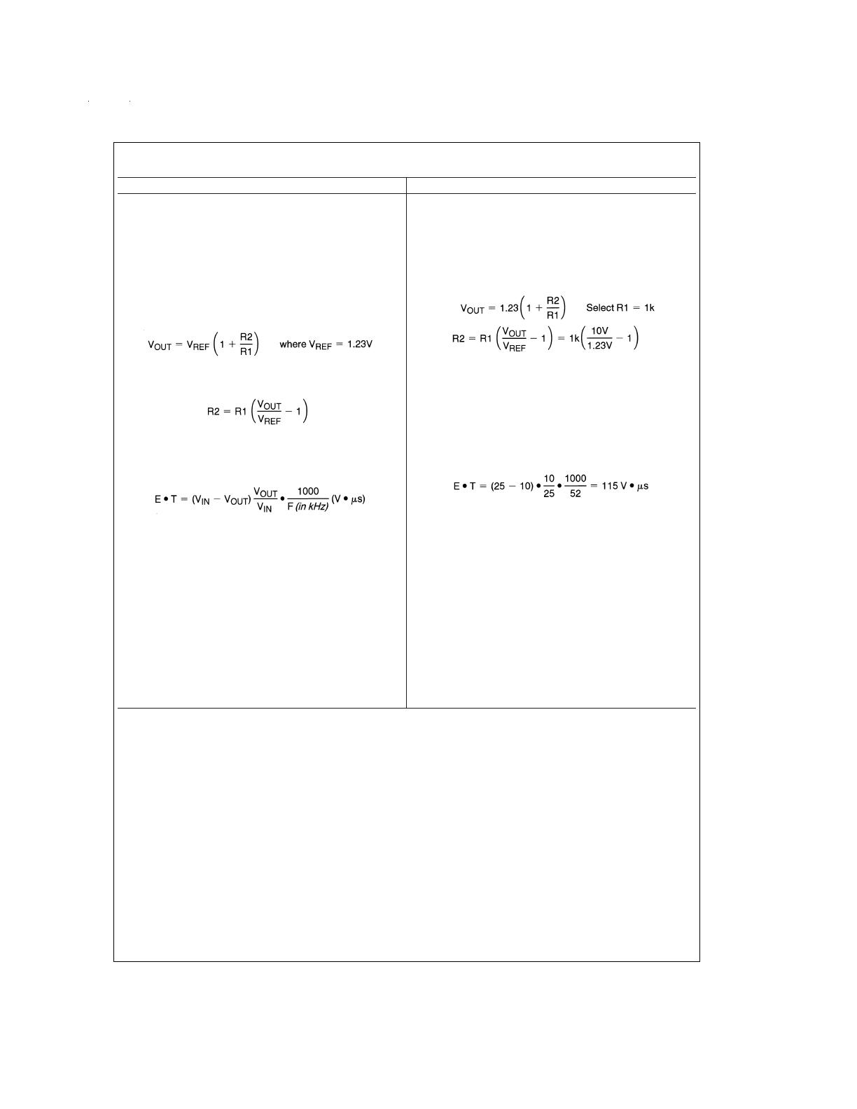
1. Programming Output Voltage
(Selecting R1 and R2, as
shown in Figure 2 )
Use the following formula to select the appropriate resistor
values.
R
1
can be between 1k and 5k.
(For best temperature coeffi-
cient and stability with time, use 1% metal film resistors)
1.Programming Output Voltage
(Selecting R1 and R2)
R2 = 1k (8.13 − 1) = 7.13k, closest 1% value is 7.15k
2. Inductor Selection (L1)
A. Calculate the inductor Volt
•
microsecond constant,
E
•
T (V
•
µs), from the following formula:
B. Use the E
•
T value from the previous formula and match
it with the E
•
T number on the vertical axis of the Inductor
Value Selection Guide shown in
Figure 7
.
C. On the horizontal axis, select the maximum load current.
D. Identify the inductance region intersected by the E
•
T
value and the maximum load current value, and note the in-
ductor code for that region.
E. Identify the inductor value from the inductor code, and se-
lect an appropriate inductor from the table shown in
Figure 9
.
Part numbers are listed for three inductor manufacturers.
The inductor chosen must be rated for operation at the
LM2575 switching frequency (52 kHz) and for a current rat-
ing of 1.15 x I
LOAD
. For additional inductor information, see
the inductor section in the application hints section of this
data sheet.
2. Inductor Selection (L1)
A. Calculate E
•
T (V
•
µs)
B. E
•
T = 115 V
•
µs
C. I
LOAD
(Max) = 1A
D. Inductance Region = H470
E. Inductor Value = 470 µH
Choose from AIE part
#430-0634, Pulse Engineering part #PE-53118, or Renco
part #RL-1961.
www.national.com
13
(Continued)
PROCEDURE (Adjustable Output Voltage Versions)
EXAMPLE (Adjustable Output Voltage Versions)
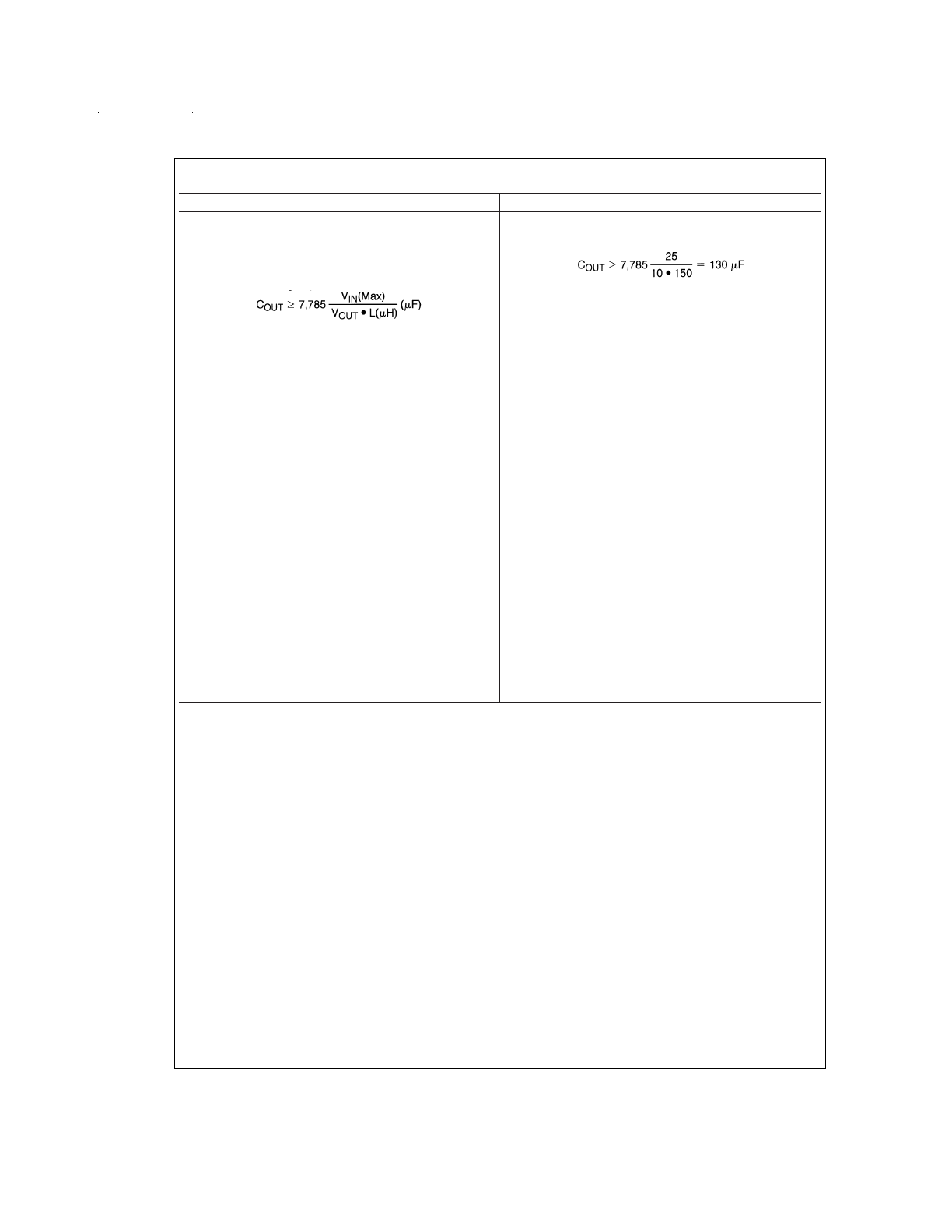
3. Output Capacitor Selection (C
OUT
)
A. The value of the output capacitor together with the induc-
tor defines the dominate pole-pair of the switching regulator
loop. For stable operation, the capacitor must satisfy the fol-
lowing requirement:
The above formula yields capacitor values between 10 µF
and 2000 µF that will satisfy the loop requirements for stable
operation. But to achieve an acceptable output ripple volt-
age, (approximately 1% of the output voltage) and transient
response, the output capacitor may need to be several times
larger than the above formula yields.
B. The capacitor’s voltage rating should be at last 1.5 times
greater than the output voltage. For a 10V regulator, a rating
of at least 15V or more is recommended.
Higher voltage electrolytic capacitors generally have lower
ESR numbers, and for this reasion it may be necessary to
select a capacitor rate for a higher voltage than would nor-
mally be needed.
3. Output Capacitor Selection (C
OUT
)
A.
However, for acceptable output ripple voltage select
C
OUT
≥
220 µF
C
OUT
= 220 µF electrolytic capacitor
4. Catch Diode Selection (D1)
A. The catch-diode current rating must be at least 1.2 times
greater than the maximum load current. Also, if the power
supply design must withstand a continuous output short, the
diode should have a current rating equal to the maximum
current limit of the LM2575. The most stressful condition for
this diode is an overload or shorted output. See diode selec-
tion guide in
Figure 8
.
B. The reverse voltage rating of the diode should be at least
1.25 times the maximum input voltage.
4. Catch Diode Selection (D1)
A. For this example, a 3A current rating is adequate.
B. Use a 40V MBR340 or 31DQ04 Schottky diode, or any of
the suggested fast-recovery diodes in
Figure 8
.
5. Input Capacitor (C
IN
)
An aluminum or tantalum electrolytic bypass capacitor lo-
cated close to the regulator is needed for stable operation.
5. Input Capacitor (C
IN
)
A 100 µF aluminum electrolytic capacitor located near the in-
put and ground pins provides sufficient bypassing.
To further simplify the buck regulator design procedure, National Semiconductor is making available computer design software to
be used with the Simple Switcher line of switching regulators. Switchers Made Simple (version 3.3) is available on a (3
1
⁄
2
") dis-
kette for IBM compatible computers from a National Semiconductor sales office in your area.
www.national.com
14
(Continued)
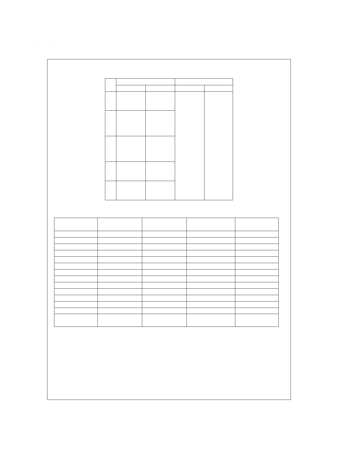
V
R
Schottky
Fast Recovery
1A
3A
1A
3A
20V
1N5817
1N5820
MBR120P
MBR320
SR102
SR302
30V
1N5818
1N5821
MBR130P
MBR330
The following
diodes are
all
rated to
100V
11DF1
MUR110
HER102
The following
diodes are
all
rated to
100V
31DF1
MURD310
HER302
11DQ03
31DQ03
SR103
SR303
40V
1N5819
IN5822
MBR140P
MBR340
11DQ04
31DQ04
SR104
SR304
50V
MBR150
MBR350
11DQ05
31DQ05
SR105
SR305
60V
MBR160
MBR360
11DQ06
31DQ06
SR106
SR306
FIGURE 8. Diode Selection Guide
Inductor
Inductor
Schott
Pulse Eng.
Renco
Code
Value
(Note 15)
(Note 16)
(Note 17)
L100
100 µH
67127000
PE-92108
RL2444
L150
150 µH
67127010
PE-53113
RL1954
L220
220 µH
67127020
PE-52626
RL1953
L330
330 µH
67127030
PE-52627
RL1952
L470
470 µH
67127040
PE-53114
RL1951
L680
680 µH
67127050
PE-52629
RL1950
H150
150 µH
67127060
PE-53115
RL2445
H220
220 µH
67127070
PE-53116
RL2446
H330
330 µH
67127080
PE-53117
RL2447
H470
470 µH
67127090
PE-53118
RL1961
H680
680 µH
67127100
PE-53119
RL1960
H1000
1000 µH
67127110
PE-53120
RL1959
H1500
1500 µH
67127120
PE-53121
RL1958
H2200
2200 µH
67127130
PE-53122
RL2448
Note 15: Schott Corp., (612) 475-1173, 1000 Parkers Lake Rd., Wayzata, MN 55391.
Note 16: Pulse Engineering, (619) 674-8100, P.O. Box 12236, San Diego, CA 92112.
Note 17: Renco Electronics Inc., (516) 586-5566, 60 Jeffryn Blvd. East, Deer Park, NY 11729.
FIGURE 9. Inductor Selection by Manufacturer’s Part Number
www.national.com
15
Application Hints
INPUT CAPACITOR (C
IN
)
To maintain stability, the regulator input pin must be by-
passed with at least a 47 µF electrolytic capacitor. The ca-
pacitor’s leads must be kept short, and located near the
regulator.
If the operating temperature range includes temperatures
below −25˚C, the input capacitor value may need to be
larger. With most electrolytic capacitors, the capacitance
value decreases and the ESR increases with lower tempera-
tures and age. Paralleling a ceramic or solid tantalum ca-
pacitor will increase the regulator stability at cold tempera-
tures. For maximum capacitor operating lifetime, the
capacitor’s RMS ripple current rating should be greater than
INDUCTOR SELECTION
All switching regulators have two basic modes of operation:
continuous and discontinuous. The difference between the
two types relates to the inductor current, whether it is flowing
continuously, or if it drops to zero for a period of time in the
normal switching cycle. Each mode has distinctively different
operating characteristics, which can affect the regulator per-
formance and requirements.
The LM2575 (or any of the Simple Switcher family) can be
used for both continuous and discontinuous modes of opera-
tion.
The inductor value selection guides in
Figure 3
through
Fig-
ure 7
were designed for buck regulator designs of the con-
tinuous inductor current type. When using inductor values
shown in the inductor selection guide, the peak-to-peak in-
ductor ripple current will be approximately 20% to 30% of the
maximum DC current. With relatively heavy load currents,
the circuit operates in the continuous mode (inductor current
always flowing), but under light load conditions, the circuit
will be forced to the discontinuous mode (inductor current
falls to zero for a period of time). This discontinuous mode of
operation is perfectly acceptable. For light loads (less than
approximately 200 mA) it may be desirable to operate the
regulator in the discontinuous mode, primarily because of
the lower inductor values required for the discontinuous
mode.
The selection guide chooses inductor values suitable for
continuous mode operation, but if the inductor value chosen
is prohibitively high, the designer should investigate the pos-
sibility of discontinuous operation. The computer design soft-
ware
Switchers Made Simple
will provide all component
values for discontinuous (as well as continuous) mode of op-
eration.
Inductors are available in different styles such as pot core,
toriod, E-frame, bobbin core, etc., as well as different core
materials, such as ferrites and powdered iron. The least ex-
pensive, the bobbin core type, consists of wire wrapped on a
ferrite rod core. This type of construction makes for an inex-
pensive inductor, but since the magnetic flux is not com-
pletely contained within the core, it generates more electro-
magnetic interference (EMI). This EMI can cause problems
in sensitive circuits, or can give incorrect scope readings be-
cause of induced voltages in the scope probe.
The inductors listed in the selection chart include ferrite pot
core construction for AIE, powdered iron toroid for Pulse En-
gineering, and ferrite bobbin core for Renco.
An inductor should not be operated beyond its maximum
rated current because it may saturate. When an inductor be-
gins to saturate, the inductance decreases rapidly and the
inductor begins to look mainly resistive (the DC resistance of
the winding). This will cause the switch current to rise very
rapidly. Different inductor types have different saturation
characteristics, and this should be kept in mind when select-
ing an inductor.
The inductor manufacturer’s data sheets include current and
energy limits to avoid inductor saturation.
INDUCTOR RIPPLE CURRENT
When the switcher is operating in the continuous mode, the
inductor current waveform ranges from a triangular to a saw-
tooth type of waveform (depending on the input voltage). For
a given input voltage and output voltage, the peak-to-peak
amplitude of this inductor current waveform remains con-
stant. As the load current rises or falls, the entire sawtooth
current waveform also rises or falls. The average DC value
of this waveform is equal to the DC load current (in the buck
regulator configuration).
If the load current drops to a low enough level, the bottom of
the sawtooth current waveform will reach zero, and the
switcher will change to a discontinuous mode of operation.
This is a perfectly acceptable mode of operation. Any buck
switching regulator (no matter how large the inductor value
is) will be forced to run discontinuous if the load current is
light enough.
OUTPUT CAPACITOR
An output capacitor is required to filter the output voltage and
is needed for loop stability. The capacitor should be located
near the LM2575 using short pc board traces. Standard alu-
minum electrolytics are usually adequate, but low ESR types
are recommended for low output ripple voltage and good
stability. The ESR of a capacitor depends on many factors,
some which are: the value, the voltage rating, physical size
and the type of construction. In general, low value or low
voltage (less than 12V) electrolytic capacitors usually have
higher ESR numbers.
The amount of output ripple voltage is primarily a function of
the ESR (Equivalent Series Resistance) of the output ca-
pacitor and the amplitude of the inductor ripple current
(
∆
I
IND
). See the section on inductor ripple current in Applica-
tion Hints.
The lower capacitor values (220 µF–680 µF) will allow typi-
cally 50 mV to 150 mV of output ripple voltage, while
larger-value capacitors will reduce the ripple to approxi-
mately 20 mV to 50 mV.
Output Ripple Voltage = (
∆
I
IND
) (ESR of C
OUT
)
To further reduce the output ripple voltage, several standard
electrolytic capacitors may be paralleled, or a higher-grade
capacitor may be used. Such capacitors are often called
“high-frequency,” “low-inductance,” or “low-ESR.” These will
reduce the output ripple to 10 mV or 20 mV. However, when
operating in the continuous mode, reducing the ESR below
0.05
Ω
can cause instability in the regulator.
www.national.com
16

Application Hints
(Continued)
Tantalum capacitors can have a very low ESR, and should
be carefully evaluated if it is the only output capacitor. Be-
cause of their good low temperature characteristics, a tanta-
lum can be used in parallel with aluminum electrolytics, with
the tantalum making up 10% or 20% of the total capacitance.
The capacitor’s ripple current rating at 52 kHz should be at
least 50% higher than the peak-to-peak inductor ripple cur-
rent.
CATCH DIODE
Buck regulators require a diode to provide a return path for
the inductor current when the switch is off. This diode should
be located close to the LM2575 using short leads and short
printed circuit traces.
Because of their fast switching speed and low forward volt-
age drop, Schottky diodes provide the best efficiency, espe-
cially in low output voltage switching regulators (less than
5V). Fast-Recovery, High-Efficiency, or Ultra-Fast Recovery
diodes are also suitable, but some types with an abrupt
turn-off characteristic may cause instability and EMI prob-
lems. A fast-recovery diode with soft recovery characteristics
is a better choice. Standard 60 Hz diodes (e.g., 1N4001 or
1N5400, etc.) are also not suitable. See
Figure 8
for Schot-
tky and “soft” fast-recovery diode selection guide.
OUTPUT VOLTAGE RIPPLE AND TRANSIENTS
The output voltage of a switching power supply will contain a
sawtooth ripple voltage at the switcher frequency, typically
about 1% of the output voltage, and may also contain short
voltage spikes at the peaks of the sawtooth waveform.
The output ripple voltage is due mainly to the inductor saw-
tooth ripple current multiplied by the ESR of the output ca-
pacitor. (See the inductor selection in the application hints.)
The voltage spikes are present because of the the fast
switching action of the output switch, and the parasitic induc-
tance of the output filter capacitor. To minimize these voltage
spikes, special low inductance capacitors can be used, and
their lead lengths must be kept short. Wiring inductance,
stray capacitance, as well as the scope probe used to evalu-
ate these transients, all contribute to the amplitude of these
spikes.
An additional small LC filter (20 µH & 100 µF) can be added
to the output (as shown in
Figure 15
) to further reduce the
amount of output ripple and transients. A 10 x reduction in
output ripple voltage and transients is possible with this filter.
FEEDBACK CONNECTION
The LM2575 (fixed voltage versions) feedback pin must be
wired to the output voltage point of the switching power sup-
ply. When using the adjustable version, physically locate
both output voltage programming resistors near the LM2575
to avoid picking up unwanted noise. Avoid using resistors
greater than 100 k
Ω
because of the increased chance of
noise pickup.
ON /OFF INPUT
For normal operation, the ON /OFF pin should be grounded
or driven with a low-level TTL voltage (typically below 1.6V).
To put the regulator into standby mode, drive this pin with a
high-level TTL or CMOS signal. The ON /OFF pin can be
safely pulled up to +V
IN
without a resistor in series with it.
The ON /OFF pin should not be left open.
GROUNDING
To maintain output voltage stability, the power ground con-
nections must be low-impedance (see
Figure 2
). For the
TO-3 style package, the case is ground. For the 5-lead
TO-220 style package, both the tab and pin 3 are ground and
either connection may be used, as they are both part of the
same copper lead frame.
With the N or M packages, all the pins labeled ground, power
ground, or signal ground should be soldered directly to wide
printed circuit board copper traces. This assures both low in-
ductance connections and good thermal properties.
HEAT SINK/THERMAL CONSIDERATIONS
In many cases, no heat sink is required to keep the LM2575
junction temperature within the allowed operating range. For
each application, to determine whether or not a heat sink will
be required, the following must be identified:
1.
Maximum ambient temperature (in the application).
2.
Maximum regulator power dissipation (in application).
3.
Maximum allowed junction temperature (150˚C for the
LM1575 or 125˚C for the LM2575). For a safe, conserva-
tive design, a temperature approximately 15˚C cooler
than the maximum temperature should be selected.
4.
LM2575 package thermal resistances
θ
JA
and
θ
JC
.
Total power dissipated by the LM2575 can be estimated as
follows:
P
D
= (V
IN
) (I
Q
) + (V
O
/V
IN
) (I
LOAD
) (V
SAT
)
where I
Q
(quiescent current) and V
SAT
can be found in the
Characteristic Curves shown previously, V
IN
is the applied
minimum input voltage, V
O
is the regulated output voltage,
and I
LOAD
is the load current. The dynamic losses during
turn-on and turn-off are negligible if a Schottky type catch di-
ode is used.
When no heat sink is used, the junction temperature rise can
be determined by the following:
∆
T
J
= (P
D
) (
θ
JA
)
To arrive at the actual operating junction temperature, add
the junction temperature rise to the maximum ambient tem-
perature.
T
J
=
∆
T
J
+ T
A
If the actual operating junction temperature is greater than
the selected safe operating junction temperature determined
in step 3, then a heat sink is required.
When using a heat sink, the junction temperature rise can be
determined by the following:
∆
T
J
= (P
D
) (
θ
JC
+
θ
interface
+
θ
Heat sink
)
The operating junction temperature will be:
T
J
= T
A
+
∆
T
J
As above, if the actual operating junction temperature is
greater than the selected safe operating junction tempera-
ture, then a larger heat sink is required (one that has a lower
thermal resistance).
When using the LM2575 in the plastic DIP (N) or surface
mount (M) packages, several items about the thermal prop-
erties of the packages should be understood. The majority of
the heat is conducted out of the package through the leads,
with a minor portion through the plastic parts of the package.
Since the lead frame is solid copper, heat from the die is
readily conducted through the leads to the printed circuit
board copper, which is acting as a heat sink.
For best thermal performance, the ground pins and all the
unconnected pins should be soldered to generous amounts
www.national.com
17
Application Hints
(Continued)
of printed circuit board copper, such as a ground plane.
Large areas of copper provide the best transfer of heat to the
surrounding air. Copper on both sides of the board is also
helpful in getting the heat away from the package, even if
there is no direct copper contact between the two sides.
Thermal resistance numbers as low as 40˚C/W for the SO
package, and 30˚C/W for the N package can be realized with
a carefully engineered pc board.
Included on the
Switchers Made Simple
design software is
a more precise (non-linear) thermal model that can be used
to determine junction temperature with different input-output
parameters or different component values. It can also calcu-
late the heat sink thermal resistance required to maintain the
regulators junction temperature below the maximum operat-
ing temperature.
Additional Applications
INVERTING REGULATOR
Figure 10
shows a LM2575-12 in a buck-boost configuration
to generate a negative 12V output from a positive input volt-
age. This circuit bootstraps the regulator’s ground pin to the
negative output voltage, then by grounding the feedback pin,
the regulator senses the inverted output voltage and regu-
lates it to −12V.
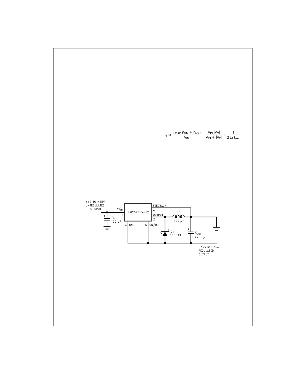
For an input voltage of 12V or more, the maximum available
output current in this configuration is approximately 0.35A. At
lighter loads, the minimum input voltage required drops to
approximately 4.7V.
The switch currents in this buck-boost configuration are
higher than in the standard buck-mode design, thus lowering
the available output current. Also, the start-up input current
of the buck-boost converter is higher than the standard
buck-mode regulator, and this may overload an input power
source with a current limit less than 1.5A. Using a delayed
turn-on or an undervoltage lockout circuit (described in the
next section) would allow the input voltage to rise to a high
enough level before the switcher would be allowed to turn
on.
Because of the structural differences between the buck and
the buck-boost regulator topologies, the buck regulator de-
sign procedure section can not be used to to select the in-
ductor or the output capacitor. The recommended range of
inductor values for the buck-boost design is between 68 µH
and 220 µH, and the output capacitor values must be larger
than what is normally required for buck designs. Low input
voltages or high output currents require a large value output
capacitor (in the thousands of micro Farads).
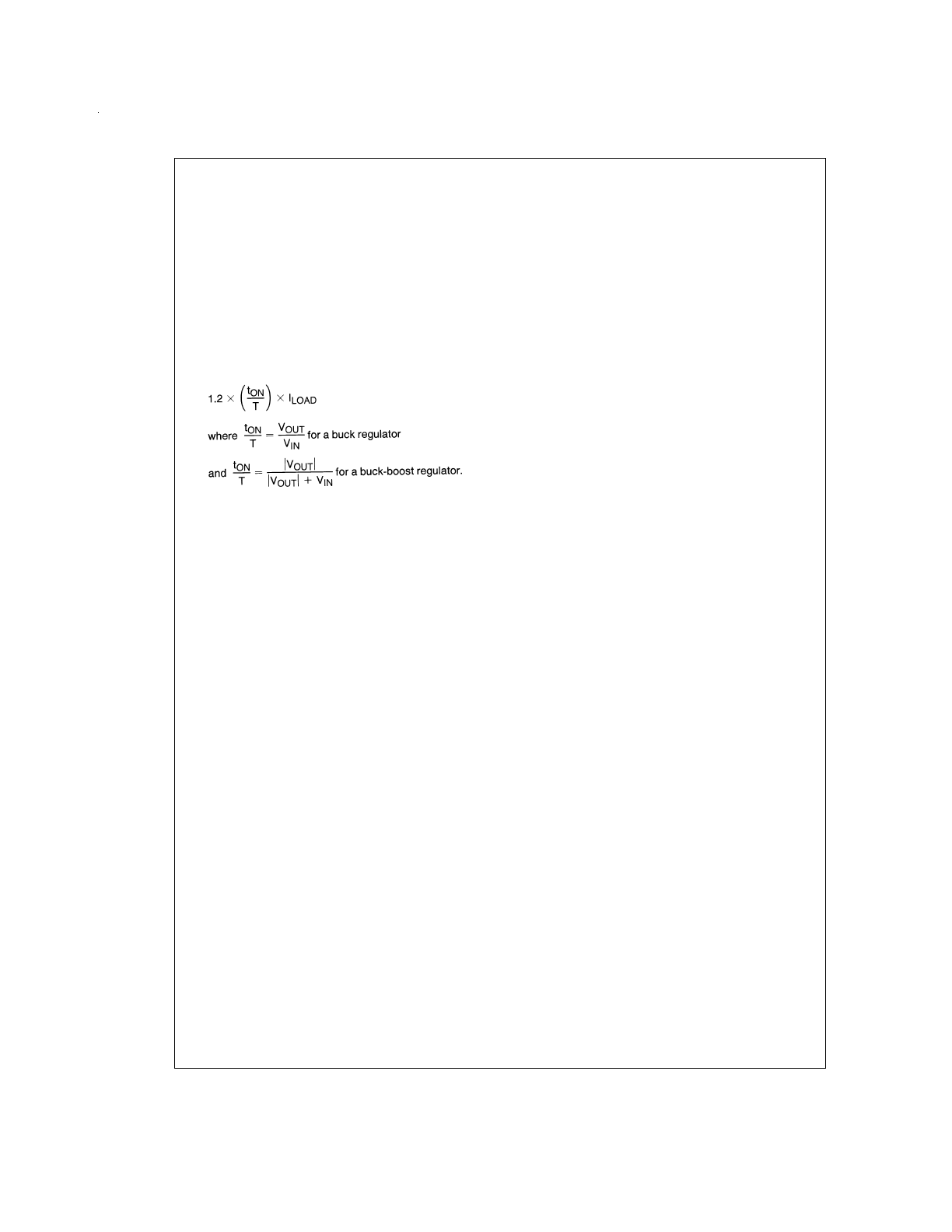
The peak inductor current, which is the same as the peak
switch current, can be calculated from the following formula:
Where f
osc
= 52 kHz. Under normal continuous inductor cur-
rent operating conditions, the minimum V
IN
represents the
worst case. Select an inductor that is rated for the peak cur-
rent anticipated.
Also, the maximum voltage appearing across the regulator is
the absolute sum of the input and output voltage. For a −12V
output, the maximum input voltage for the LM2575 is +28V,
or +48V for the LM2575HV.
The
Switchers Made Simple
(version 3.3) design software
can be used to determine the feasibility of regulator designs
using different topologies, different input-output parameters,
different components, etc.
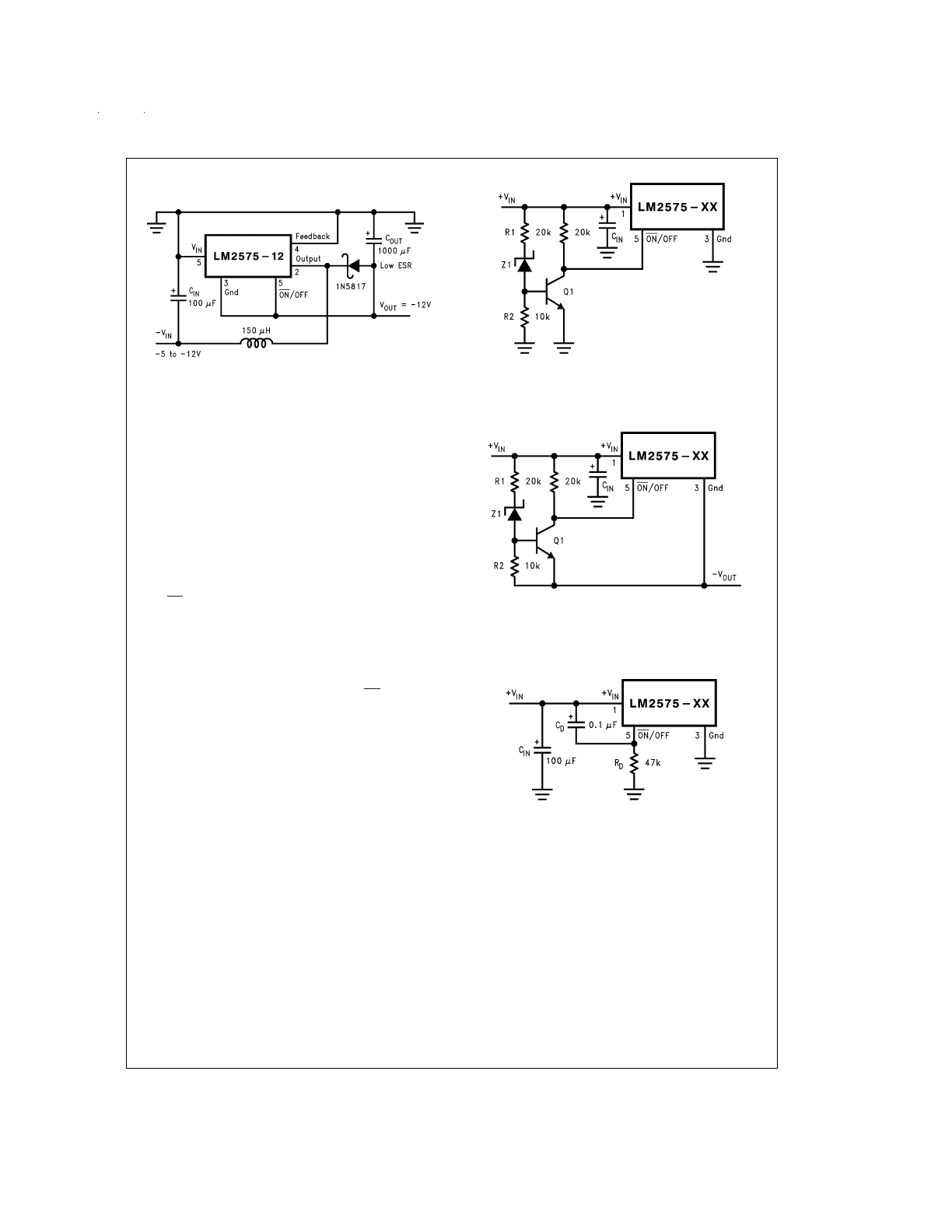
NEGATIVE BOOST REGULATOR
Another variation on the buck-boost topology is the negative
boost configuration. The circuit in
Figure 11
accepts an input
voltage ranging from −5V to −12V and provides a regulated
−12V output. Input voltages greater than −12V will cause the
output to rise above −12V, but will not damage the regulator.
Because of the boosting function of this type of regulator, the
switch current is relatively high, especially at low input volt-
ages. Output load current limitations are a result of the maxi-
mum current rating of the switch. Also, boost regulators can
not provide current limiting load protection in the event of a
shorted load, so some other means (such as a fuse) may be
necessary.
DS011475-15
FIGURE 10. Inverting Buck-Boost Develops −12V
www.national.com
18
Additional Applications
(Continued)
UNDERVOLTAGE LOCKOUT
In some applications it is desirable to keep the regulator off
until the input voltage reaches a certain threshold. An under-
voltage lockout circuit which accomplishes this task is shown
in
Figure 12
, while
Figure 13
shows the same circuit applied
to a buck-boost configuration. These circuits keep the regu-
lator off until the input voltage reaches a predetermined
level.
V
TH
≈
V
Z1
+ 2V
BE
(Q1)
DELAYED STARTUP
The ON /OFF pin can be used to provide a delayed startup
feature as shown in
Figure 14
. With an input voltage of 20V
and for the part values shown, the circuit provides approxi-
mately 10 ms of delay time before the circuit begins switch-
ing. Increasing the RC time constant can provide longer de-
lay times. But excessively large RC time constants can
cause problems with input voltages that are high in 60 Hz or
120 Hz ripple, by coupling the ripple into the ON /OFF pin.
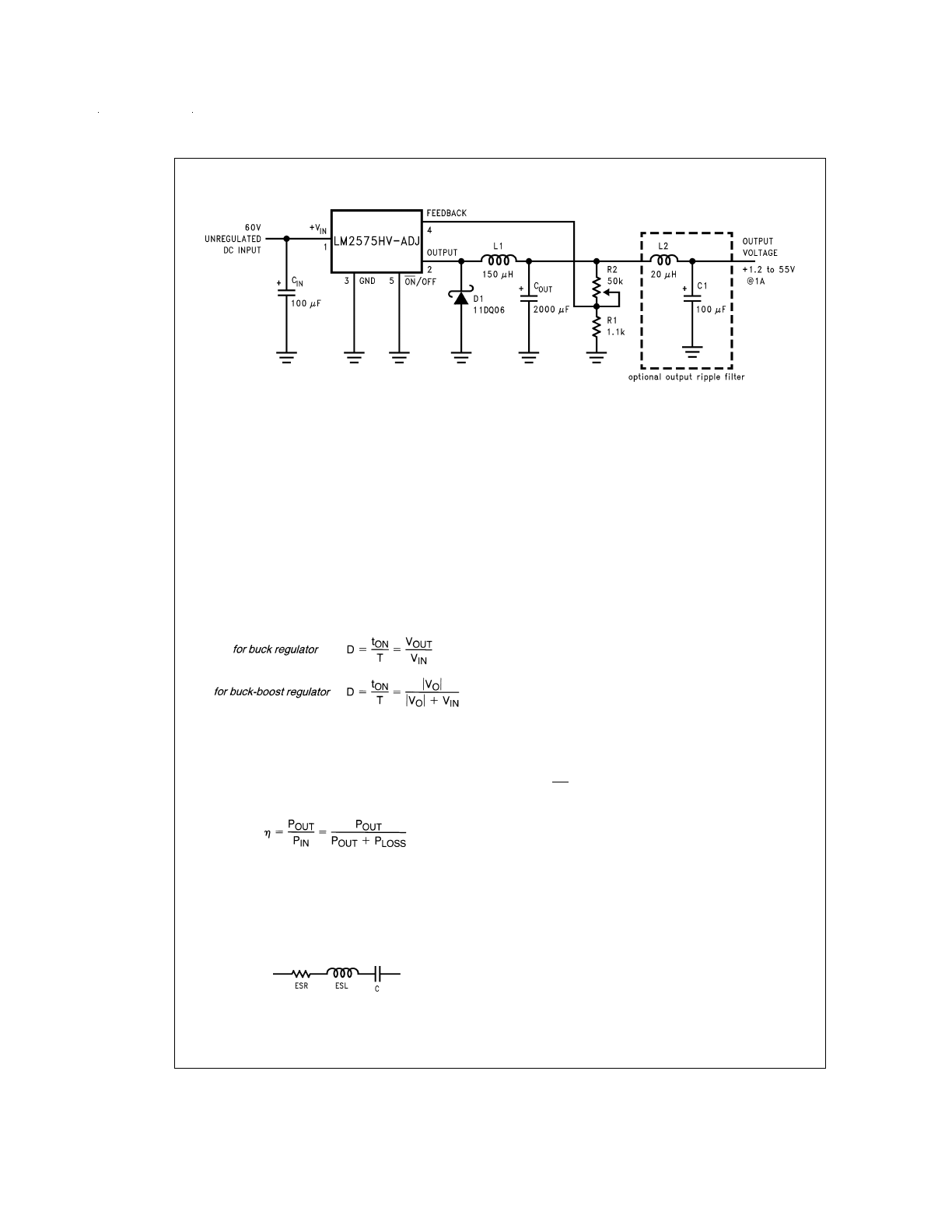
ADJUSTABLE OUTPUT, LOW-RIPPLE
POWER SUPPLY
A 1A power supply that features an adjustable output voltage
is shown in
Figure 15
. An additional L-C filter that reduces
the output ripple by a factor of 10 or more is included in this
circuit.
DS011475-16
Typical Load Current
200 mA for V
IN
= −5.2V
500 mA for V
IN
= −7V
Note: Pin numbers are for TO-220 package.
FIGURE 11. Negative Boost
DS011475-17
Note: Complete circuit not shown.
Note: Pin numbers are for the TO-220 package.
FIGURE 12. Undervoltage Lockout for Buck Circuit
DS011475-18
Note: Complete circuit not shown (see
Figure 10
).
Note: Pin numbers are for the TO-220 package.
FIGURE 13. Undervoltage Lockout
for Buck-Boost Circuit
DS011475-19
Note: Complete circuit not shown.
Note: Pin numbers are for the TO-220 package.
FIGURE 14. Delayed Startup
www.national.com
19
Additional Applications
(Continued)
Definition of Terms
BUCK REGULATOR
A switching regulator topology in which a higher voltage is
converted to a lower voltage. Also known as a step-down
switching regulator.
BUCK-BOOST REGULATOR
A switching regulator topology in which a positive voltage is
converted to a negative voltage without a transformer.
DUTY CYCLE (D)
Ratio of the output switch’s on-time to the oscillator period.
CATCH DIODE OR CURRENT STEERING DIODE
The diode which provides a return path for the load current
when the LM2575 switch is OFF.
EFFICIENCY (
η
)
The proportion of input power actually delivered to the load.
CAPACITOR EQUIVALENT SERIES RESISTANCE (ESR)
The purely resistive component of a real capacitor’s imped-
ance (see
Figure 16
). It causes power loss resulting in ca-
pacitor heating, which directly affects the capacitor’s operat-
ing lifetime. When used as a switching regulator output filter,
higher ESR values result in higher output ripple voltages.
Most standard aluminum electrolytic capacitors in the
100
µF–1000
µF
range
have
0.5
Ω
to
0.1
Ω
ESR.
Higher-grade capacitors (“low-ESR”, “high-frequency”, or
“low-inductance”’) in the 100 µF–1000 µF range generally
have ESR of less than 0.15
Ω
.
EQUIVALENT SERIES INDUCTANCE (ESL)
The pure inductance component of a capacitor (see
Figure
16
). The amount of inductance is determined to a large ex-
tent on the capacitor’s construction. In a buck regulator, this
unwanted inductance causes voltage spikes to appear on
the output.
OUTPUT RIPPLE VOLTAGE
The AC component of the switching regulator’s output volt-
age. It is usually dominated by the output capacitor’s ESR
multiplied by the inductor’s ripple current (
∆
I
IND
). The
peak-to-peak value of this sawtooth ripple current can be de-
termined by reading the Inductor Ripple Current section of
the Application hints.
CAPACITOR RIPPLE CURRENT
RMS value of the maximum allowable alternating current at
which a capacitor can be operated continuously at a speci-
fied temperature.
STANDBY QUIESCENT CURRENT (I
STBY
)
Supply current required by the LM2575 when in the standby
mode (ON /OFF pin is driven to TTL-high voltage, thus turn-
ing the output switch OFF).
INDUCTOR RIPPLE CURRENT (
∆
I
IND
)
The peak-to-peak value of the inductor current waveform,
typically a sawtooth waveform when the regulator is operat-
ing in the continuous mode (vs. discontinuous mode).
CONTINUOUS/DISCONTINUOUS MODE OPERATION
Relates to the inductor current. In the continuous mode, the
inductor current is always flowing and never drops to zero,
vs. the discontinuous mode, where the inductor current
drops to zero for a period of time in the normal switching
cycle.
DS011475-20
Note: Pin numbers are for the TO-220 package.
FIGURE 15. 1.2V to 55V Adjustable 1A Power Supply with Low Output Ripple
DS011475-21
FIGURE 16. Simple Model of a Real Capacitor
www.national.com
20

Definition of Terms
(Continued)
INDUCTOR SATURATION
The condition which exists when an inductor cannot hold any
more magnetic flux. When an inductor saturates, the induc-
tor appears less inductive and the resistive component domi-
nates. Inductor current is then limited only by the DC resis-
tance of the wire and the available source current.
OPERATING VOLT MICROSECOND CONSTANT (E
•
T
op
)
The product (in VoIt
•
µs) of the voltage applied to the inductor
and the time the voltage is applied. This E
•
T
op
constant is a
measure of the energy handling capability of an inductor and
is dependent upon the type of core, the core area, the num-
ber of turns, and the duty cycle.
www.national.com
21
Physical Dimensions
inches (millimeters) unless otherwise noted
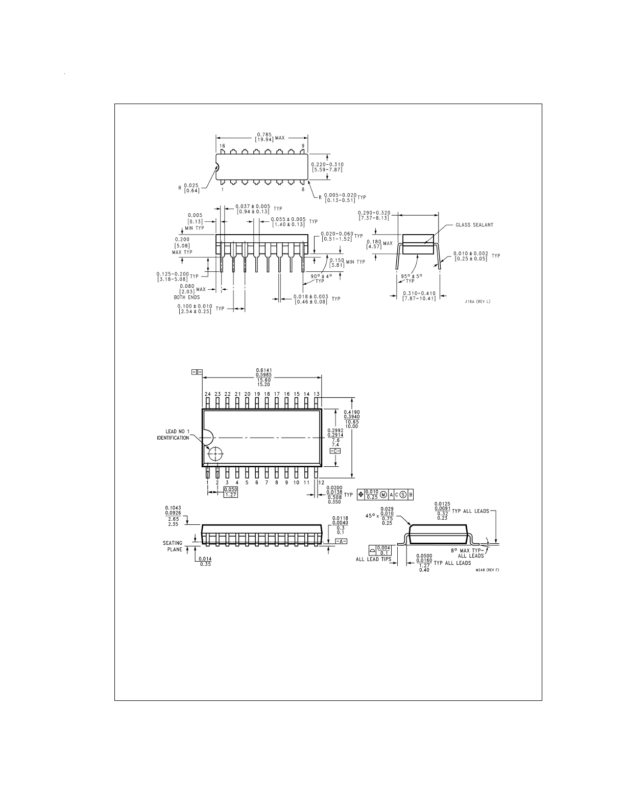
16-Lead Ceramic Dual-in-Line (J)
Order Number LM1575J-3.3/883, LM1575J-5.0/883,
LM1575J-12/883, LM1575J-15/883, or LM1575J-ADJ/883
NS Package Number J16A
14-Lead Wide Surface Mount (WM)
Order Number LM2575M-5.0, LM2575HVM-5.0, LM2575M-12,
LM2575HVM-12, LM2575M-15, LM2575HVM-15,
LM2575M-ADJ or LM2575HVM-ADJ
NS Package Number M24B
www.national.com
22
Physical Dimensions
inches (millimeters) unless otherwise noted (Continued)
16-Lead Molded DIP (N)
Order Number LM2575N-5.0, LM2575HVN-5.0, LM2575N-12, LM2575HVN-12,
LM2575N-15, LM2575HVN-15, LM2575N-ADJ or LM2575HVN-ADJ
NS Package Number N16A
5-Lead TO-220 (T)
Order Number LM2575T-3.3, LM2575HVT-3.3, LM2575T-5.0, LM2575HVT-5.0, LM2575T-12,
LM2575HVT-12, LM2575T-15, LM2575HVT-15, LM2575T-ADJ or LM2575HVT-ADJ
NS Package Number T05A
www.national.com
23
Physical Dimensions
inches (millimeters) unless otherwise noted (Continued)
TO-263, Molded, 5-Lead Surface Mount
Order Number LM2575S-3.3, LM2575HVS-3.3, LM2575S-5.0, LM2575HVS-5.0, LM2575S-12,
LM2575HVS-12, LM2575S-15, LM2575HVS-15, LM2575S-ADJ or LM2575HVS-ADJ
NS Package Number TS5B
www.national.com
24
Physical Dimensions
inches (millimeters) unless otherwise noted (Continued)
LIFE SUPPORT POLICY
NATIONAL’S PRODUCTS ARE NOT AUTHORIZED FOR USE AS CRITICAL COMPONENTS IN LIFE SUPPORT
DEVICES OR SYSTEMS WITHOUT THE EXPRESS WRITTEN APPROVAL OF THE PRESIDENT AND GENERAL
COUNSEL OF NATIONAL SEMICONDUCTOR CORPORATION. As used herein:
1. Life support devices or systems are devices or
systems which, (a) are intended for surgical implant
into the body, or (b) support or sustain life, and
whose failure to perform when properly used in
accordance with instructions for use provided in the
labeling, can be reasonably expected to result in a
significant injury to the user.
2. A critical component is any component of a life
support device or system whose failure to perform
can be reasonably expected to cause the failure of
the life support device or system, or to affect its
safety or effectiveness.
National Semiconductor
Corporation
Americas
Tel: 1-800-272-9959
Fax: 1-800-737-7018
Email: support@nsc.com
National Semiconductor
Europe
Fax: +49 (0) 1 80-530 85 86
Email: europe.support@nsc.com
Deutsch Tel: +49 (0) 1 80-530 85 85
English
Tel: +49 (0) 1 80-532 78 32
Français Tel: +49 (0) 1 80-532 93 58
Italiano
Tel: +49 (0) 1 80-534 16 80
National Semiconductor
Asia Pacific Customer
Response Group
Tel: 65-2544466
Fax: 65-2504466
Email: sea.support@nsc.com
National Semiconductor
Japan Ltd.
Tel: 81-3-5639-7560
Fax: 81-3-5639-7507
www.national.com
Bent, Staggered 5-Lead TO-220 (T)
Order Number LM2575T-3.3 Flow LB03, LM2575HVT-3.3 Flow LB03,
LM2575T-5.0 Flow LB03, LM2575HVT-5.0 Flow LB03,
LM2575T-12 Flow LB03, LM2575HVT-12 Flow LB03,
LM2575T-15 Flow LB03, LM2575HVT-15 Flow LB03,
LM2575T-ADJ Flow LB03 or LM2575HVT-ADJ Flow LB03
NS Package Number T05D
LM1575/LM2575/LM2575HV
Series
SIMPLE
SWITCHER
1A
Step-Down
V
oltage
Regulator
National does not assume any responsibility for use of any circuitry described, no circuit patent licenses are implied and National reserves the right at any time without notice to change said circuitry and specifications.