
TL/H/5706
LM139/LM239/LM339/LM2901/LM3302
Low
Power
Low
Offset
Voltage
Quad
Comparators
November 1994
LM139/LM239/LM339/LM2901/LM3302
Low Power Low Offset Voltage Quad Comparators
General Description
The LM139 series consists of four independent precision
voltage comparators with an offset voltage specification as
low as 2 mV max for all four comparators. These were de-
signed specifically to operate from a single power supply
over a wide range of voltages. Operation from split power
supplies is also possible and the low power supply current
drain is independent of the magnitude of the power supply
voltage. These comparators also have a unique characteris-
tic in that the input common-mode voltage range includes
ground, even though operated from a single power supply
voltage.
Application areas include limit comparators, simple analog
to digital converters; pulse, squarewave and time delay gen-
erators; wide range VCO; MOS clock timers; multivibrators
and high voltage digital logic gates. The LM139 series was
designed to directly interface with TTL and CMOS. When
operated from both plus and minus power supplies, they will
directly interface with MOS logicÐ where the low power
drain of the LM339 is a distinct advantage over standard
comparators.
Advantages
Y
High precision comparators
Y
Reduced V
OS
drift over temperature
Y
Eliminates need for dual supplies
Y
Allows sensing near GND
Y
Compatible with all forms of logic
Y
Power drain suitable for battery operation
Features
Y
Wide supply voltage range
LM139 series,
2 V
DC
to 36 V
DC
or
g
1 V
DC
to
g
18 V
DC
LM139A series, LM2901
2 V
DC
to 28 V
DC
LM3302
or
g
1 V
DC
to
g
14 V
DC
Y
Very low supply current drain (0.8 mA) Ð independent
of supply voltage
Y
Low input biasing current
25 nA
Y
Low input offset current
g
5 nA
and offset voltage
g
3 mV
Y
Input common-mode voltage range includes GND
Y
Differential input voltage range equal to the power
supply voltage
Y
Low output saturation voltage
250 mV at 4 mA
Y
Output voltage compatible with TTL, DTL, ECL, MOS
and CMOS logic systems
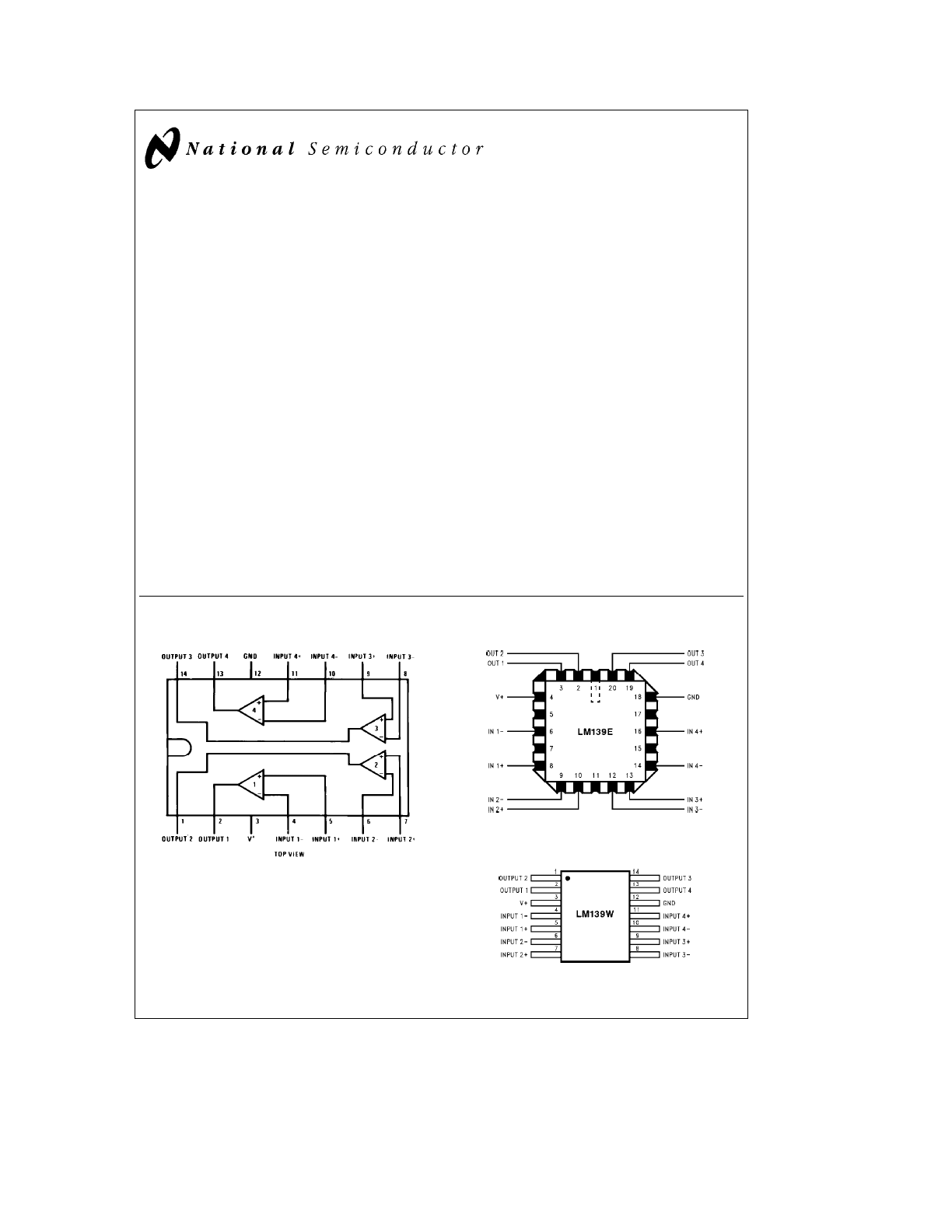
Connection Diagrams
Dual-In-Line Package
TL/H/5706 – 2
Order Number LM139J, LM139J/883
*, LM139AJ,
LM139AJ/883
**, LM239J, LM239AJ, LM339J,
See NS Package Number J14A
Order Number LM339AM, LM339M or LM2901M
See NS Package Number M14A
Order Number LM339N, LM339AN,
LM2901N or LM3302N
See NS Package Number N14A
*Available per JM38510/11201
**Available per SMD
Ý
5962-8873901
TL/H/5706 – 26
Order Number LM139AE/883 or LM139E/883
See NS Package Number E20A
TL/H/5706 – 27
Order Number LM139AW/883 or LM139W/883
*
See NS Package Number W14B
C1995 National Semiconductor Corporation
RRD-B30M115/Printed in U. S. A.
Absolute
Maximum
Ratings
(Note
10)
If
Military/Aerospace
specified
devices
are
required,
please
contact
the
National
Semiconductor
Sales
Office/Distributors
for
availability
and
specifications.
LM139/LM239/LM339
LM139A/LM239A/LM339A
LM3302
LM2901
Supply
Voltage,
V
a
36
V
DC
or
g
18
V
DC
28
V
DC
or
g
14
V
DC
Differential
Input
Voltage
(Note
8)
36
V
DC
28
V
DC
Input
Voltage
b
0.3
V
DC
to
a
36
V
DC
b
0.3
V
DC
to
a
28
V
DC
Input
Current
(V
IN
k
b
0.3
V
DC
),
(Note
3)
50
mA
50
mA
Power
Dissipation
(Note
1)
Molded
DIP
1050
mW
1050
mW
Cavity
DIP
1190
mW
Small
Outline
Package
760
mW
Output
Short-Circuit
to
GND,
(Note
2)
Continuous
Continuous
Storage
Temperature
Range
b
65
§
Ct
o
a
150
§
C
b
65
§
Ct
o
a
150
§
C
Lead
Temperature
(Soldering,
10
seconds)
260
§
C
260
§
C
LM139/LM239/LM339
LM139A/LM239A/LM339A
LM3302
LM2901
Operating
Temperature
Range
b
40
§
Ct
o
a
85
§
C
LM339/LM339A
0
§
Ct
o
a
70
§
C
LM239/LM239A
b
25
§
Ct
o
a
85
§
C
LM2901
b
40
§
Ct
o
a
85
§
C
LM139/LM139A
b
55
§
Ct
o
a
125
§
C
Soldering
Information
Dual-In-Line
Package
Soldering
(10
seconds)
260
§
C
260
§
C
Small
Outline
Package
Vapor
Phase
(60
seconds)
215
§
C
215
§
C
Infrared
(15
seconds)
220
§
C
220
§
C
See
AN-450
‘‘Surface
Mounting
Methods
and
Their
Effect
on
Product
Reliability’’
for
other
methods
of
soldering
surface
mount
devices.
ESD
rating
(1.5
k
X
in
series
with
100
pF)
600V
600V
Electrical
Characteristics
(V
a
e
5V
DC
,T
A
e
25
§
C,
unless
otherwise
stated)
Parameter
Conditions
LM139A
LM239A,
LM339A
LM139
LM239,
LM339
LM2901
LM3302
Units
Min
Typ
Max
Min
Typ
Max
Min
Typ
Max
Min
Typ
Max
Min
Typ
Max
Min
Typ
Max
Input
Offset
Voltage
(Note
9)
1.0
2.0
1.0
2.0
2.0
5.0
2.0
5.0
2.0
7.0
3
2
0
m
V
DC
Input
Bias
Current
I
IN(
a
)
or
I
IN(
b
)
with
Output
in
25
100
25
250
25
100
25
250
25
250
25
500
nA
DC
Linear
Range,
(Note
5),
V
CM
e
0V
Input
Offset
Current
I
IN(
a
)
b
I
IN(
b
)
,V
CM
e
0V
3.0
25
5.0
50
3.0
25
5.0
50
5
5
0
3
100
nA
DC
Input
Common-Mode
V
a
e
30
V
DC
(LM3302,
V
a
e
28
V
DC
)0
V
a
b
1.5
0
V
a
b
1.5
0
V
a
b
1.5
0
V
a
b
1.5
0
V
a
b
1.5
0
V
a
b
1.5
V
DC
Voltage
Range
(Note
6)
Supply
Current
R
L
e
%
on
all
Comparators,
0.8
2.0
0.8
2.0
0.8
2.0
0.8
2.0
0.8
2.0
0.8
2.0
mA
DC
R
L
e
%
,V
a
e
36V,
1.0
2.5
1.0
2.5
1.0
2.5
1.0
2.5
1.0
2.5
mA
DC
(LM3302,
V
a
e
28
V
DC
)
Voltage
Gain
R
L
t
15
k
X
,V
a
e
15
V
DC
50
200
50
200
50
200
50
200
25
100
2
3
0
V/mV
V
o
e
1V
DC
to
11
V
DC
Large
Signal
V
IN
e
TTL
Logic
Swing,
V
REF
e
300
300
300
300
300
300
ns
Response
Time
1.4
V
DC
,V
RL
e
5V
DC
,R
L
e
5.1
k
X
,
Response
Time
V
RL
e
5V
DC
,R
L
e
5.1
k
X
,
1.3
1.3
1.3
1.3
1.3
1.3
m
s
(Note
7)
Output
Sink
Current
V
IN(
b
)
e
1V
DC
,V
IN(
a
)
e
0,
6.0
16
6.0
16
6.0
16
6.0
16
6.0
16
6.0
16
mA
DC
V
O
s
1.5
V
DC
2
Electrical
Characteristics
(V
a
e
5V
DC
,T
A
e
25
§
C,
unless
otherwise
stated)
(Continued)
Parameter
Conditions
LM139A
LM239A,
LM339A
LM139
LM239,
LM339
LM2901
LM3302
Units
Min
Typ
Max
Min
Typ
Max
Min
Typ
Max
Min
Typ
Max
Min
Typ
Max
Min
Typ
Max
Saturation
Voltage
V
IN(
b
)
e
1V
DC
,V
IN(
a
)
e
0,
250
400
250
400
250
400
250
400
250
400
250
500
mV
DC
I
SINK
s
4m
A
Output
Leakage
V
IN(
a
)
e
1V
DC
,V
IN(
b
)
e
0,
0.1
0.1
0.1
0.1
0.1
0.1
nA
DC
Current
V
O
e
5V
DC
Electrical
Characteristics
(V
a
e
5.0
V
DC
,
Note
4)
Parameter
Conditions
LM139A
LM239A,
LM339A
LM139
LM239,
LM339
LM2901
LM3302
Units
Min
Typ
Max
Min
Typ
Max
Min
Typ
Max
Min
Typ
Max
Min
Typ
Max
Min
Typ
Max
Input
Offset
Voltage
(Note
9)
4.0
4.0
9.0
9.0
9
1
5
4
0
m
V
DC
Input
Offset
Current
I
IN(
a
)
b
I
IN(
b
)
,V
CM
e
0V
100
150
100
150
50
200
300
nA
DC
Input
Bias
Current
I
IN(
a
)
or
I
IN(
b
)
with
Output
in
300
400
300
400
200
500
1000
nA
DC
Linear
Range,
V
CM
e
0V
(Note
5)
Input
Common-Mode
V
a
e
30
V
DC
(LM3302,
V
a
e
28
V
DC
)0
V
a
b
2.0
0
V
a
b
2.0
0
V
a
b
2.0
V
a
b
2.0
0
V
a
b
2.0
0
V
a
b
2.0
V
DC
Voltage
Range
(Note
6)
Saturation
Voltage
V
IN(
b
)
e
1V
DC
,V
IN(
a
)
e
0,
700
700
700
700
400
700
700
mV
DC
I
SINK
s
4m
A
Output
Leakage
Current
V
IN(
a
)
e
1V
DC
,V
IN(
b
)
e
0,
1.0
1.0
1.0
1.0
1.0
1.0
m
A
DC
V
O
e
30
V
DC
,
(LM3302,
V
O
e
28
V
DC
)
Differential
Input
Voltage
Keep
all
V
IN
’s
t
0V
DC
(or
V
b
,
3
6
3
63
63
63
62
8
V
DC
if
used),
(Note
8)
Note
1:
For
operating
at
high
temperatures,
the
LM339/LM339A,
LM2901,
LM3302
must
be
derated
based
on
a
125
§
C
maximum
junction
temperature
and
a
thermal
resistance
of
95
§
C/W
which
applies
for
the
device
soldered
in
a
printed
circuit
board,
operating
in
a
still
air
ambient.
The
LM239
and
LM139
must
be
derated
based
on
a
150
§
C
maximum
junction
temperature.
The
low
bias
dissipation
and
the
‘‘ON-OFF’’
characteristic
of
the
outputs
keeps
the
chip
dissipation
very
small
(P
D
s
100
mW),
provided
the
output
transistors
are
allowed
to
saturate.
Note
2:
Short
circuits
from
the
output
to
V
a
can
cause
excessive
heating
and
eventual
destruction.
When
considering
short
circuits
to
ground,
the
maximum
output
current
is
approximately
20
mA
independent
of
the
magnitude
of
V
a
.
Note
3:
This
input
current
will
only
exist
when
the
voltage
at
any
of
the
input
leads
is
driven
negative.
It
is
due
to
the
collector-base
junction
of
the
input
PNP
transistors
becoming
forward
biased
and
thereby
acting
as
input
diode
clamps.
In
addition
to
this
diode
action,
there
is
also
lateral
NPN
parasitic
transistor
action
on
the
IC
chip.
This
transistor
action
can
cause
the
output
voltages
of
the
comparators
to
go
to
the
V
a
voltage
level
(or
to
ground
for
a
large
overdrive)
for
the
time
duration
that
an
input
is
driven
negative.
This
is
not
destructive
and
normal
output
states
will
re-establish
when
the
input
voltage,
which
was
negative,
again
returns
to
a
value
greater
than
b
0.3
V
DC
(at
25
§
)C.
Note
4:
These
specifications
are
limited
to
b
55
§
C
s
T
A
s
a
125
§
C,
for
the
LM139/LM139A.
With
the
LM239/LM239A,
all
temperature
specifications
are
limited
to
b
25
§
C
s
T
A
s
a
85
§
C,
the
LM339/LM339A
temperature
specifications
are
limited
to
0
§
C
s
T
A
s
a
70
§
C,
and
the
LM2901,
LM3302
temperature
range
is
b
40
§
C
s
T
A
s
a
85
§
C.
Note
5:
The
direction
of
the
input
current
is
out
of
the
IC
due
to
the
PNP
input
stage.
This
current
is
essentially
constant,
independent
of
the
state
of
the
output
so
no
loading
change
exists
on
the
reference
or
input
lines.
Note
6:
The
input
common-mode
voltage
or
either
input
signal
voltage
should
not
be
allowed
to
go
negative
by
more
than
0.3V.
The
upper
end
of
the
common-mode
voltage
range
is
V
a
b
1.5V
at
25
§
C,
but
either
or
both
inputs
can
go
to
a
30
V
DC
without
damage
(25V
for
LM3302),
independent
of
the
magnitude
of
V
a
.
Note
7:
The
response
time
specified
is
a
100
mV
input
step
with
5
m
V
overdrive.
For
larger
overdrive
signals
300
ns
can
be
obtained,
see
typical
performance
characteristics
section.
Note
8:
Positive
excursions
of
input
voltage
may
exceed
the
power
supply
level.
As
long
as
the
other
voltage
remains
within
the
common-mode
range,
the
comparator
will
provide
a
proper
output
state.
The
low
input
voltage
state
must
not
be
less
than
b
0.3
V
DC
(or
0.3
V
DC
below
the
magnitude
of
the
negative
power
supply,
if
used)
(at
25
§
C).
Note
9:
At
output
switch
point,
V
O
j
1.4
V
DC
,R
S
e
0
X
with
V
a
from
5
V
DC
to
30
V
DC
;
and
over
the
full
input
common-mode
range
(0
V
DC
to
V
a
b
1.5
V
DC
),
at
25
§
C.
For
LM3302,
V
a
from
5
V
DC
to
28
V
DC
.
Note
10:
Refer
to
RETS139AX
for
LM139A
military
specifications
and
to
RETS139X
for
LM139
military
specifications.
3
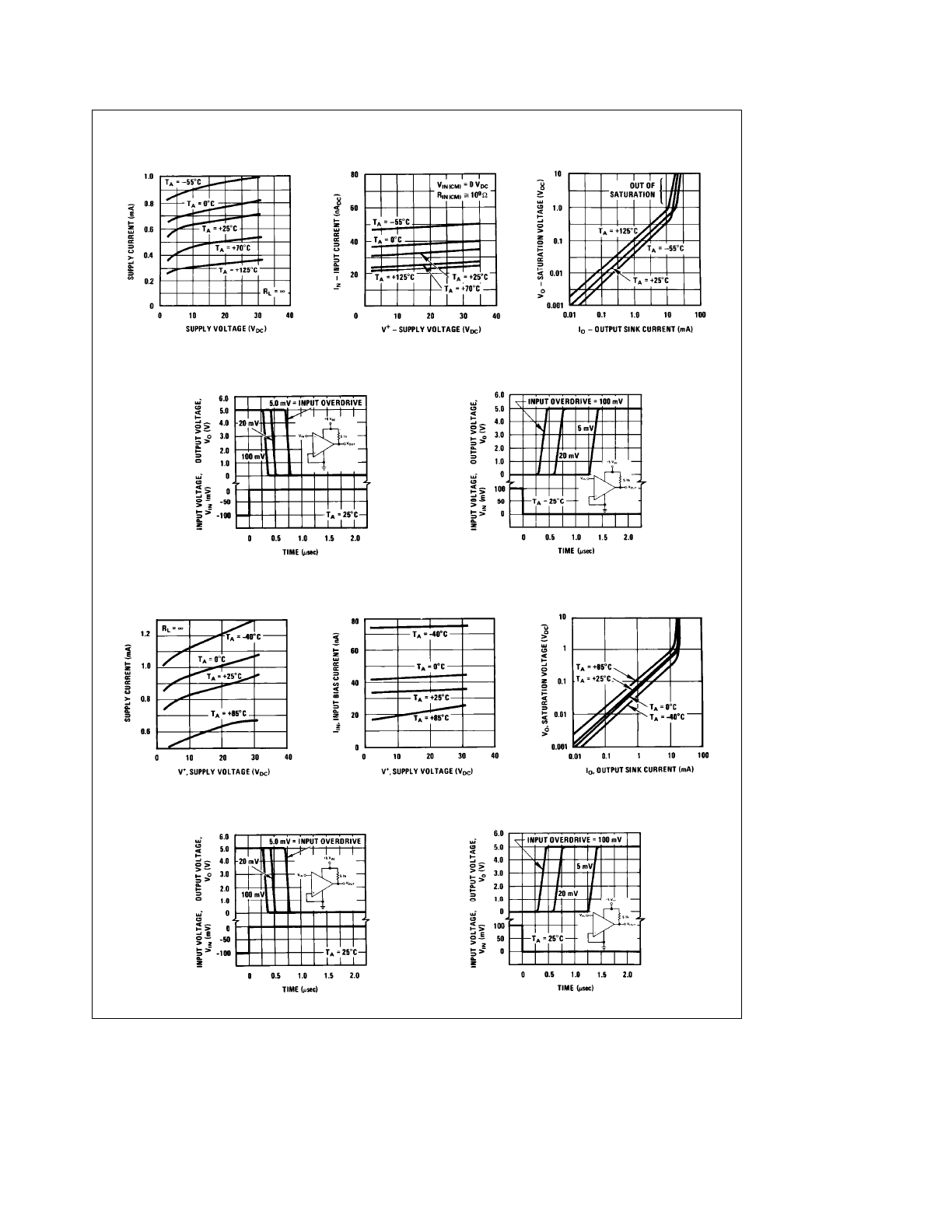
Typical Performance Characteristics
LM139/LM239/LM339, LM139A/LM239A/LM339A, LM3302
Supply Current
Input Current
Output Saturation Voltage
Response Time for Various
Input OverdrivesÐNegative
Transition
Response Time for Various
Input OverdrivesÐPositive
Transition
TL/H/5706 – 6
Typical Performance Characteristics
LM2901
Supply Current
Input Current
Output Saturation Voltage
Response Time for Various
Input Overdrives-Negative
Transition
Response Time for Various
Input Overdrives-Positive
Transition
TL/H/5706 – 7
4
Application Hints
The LM139 series are high gain, wide bandwidth devices
which, like most comparators, can easily oscillate if the out-
put lead is inadvertently allowed to capacitively couple to
the inputs via stray capacitance. This shows up only during
the output voltage transition intervals as the comparator
changes states. Power supply bypassing is not required to
solve this problem. Standard PC board layout is helpful as it
reduces stray input-output coupling. Reducing this input re-
sistors to
k
10 kX reduces the feedback signal levels and
finally, adding even a small amount (1 to 10 mV) of positive
feedback (hysteresis) causes such a rapid transition that
oscillations due to stray feedback are not possible. Simply
socketing the IC and attaching resistors to the pins will
cause input-output oscillations during the small transition in-
tervals unless hysteresis is used. If the input signal is a
pulse waveform, with relatively fast rise and fall times, hys-
teresis is not required.
All pins of any unused comparators should be grounded.
The bias network of the LM139 series establishes a drain
current which is independent of the magnitude of the power
supply voltage over the range of from 2 V
DC
to 30 V
DC
.
It is usually unnecessary to use a bypass capacitor across
the power supply line.
The differential input voltage may be larger than V
a
without
damaging the device. Protection should be provided to pre-
vent the input voltages from going negative more than
b
0.3
V
DC
(at 25
§
C). An input clamp diode can be used as shown
in the applications section.
The output of the LM139 series is the uncommitted collector
of a grounded-emitter NPN output transistor. Many collec-
tors can be tied together to provide an output OR’ing func-
tion. An output pull-up resistor can be connected to any
available power supply voltage within the permitted supply
voltage range and there is no restriction on this voltage due
to the magnitude of the voltage which is applied to the V
a
terminal of the LM139A package. The output can also be
used as a simple SPST switch to ground (when a pull-up
resistor is not used). The amount of current which the output
device can sink is limited by the drive available (which is
independent of V
a
) and the b of this device. When the
maximum current limit is reached (approximately 16 mA),
the output transistor will come out of saturation and the out-
put voltage will rise very rapidly. The output saturation volt-
age is limited by the approximately 60X R
SAT
of the output
transistor. The low offset voltage of the output transistor (1
mV) allows the output to clamp essentially to ground level
for small load currents.
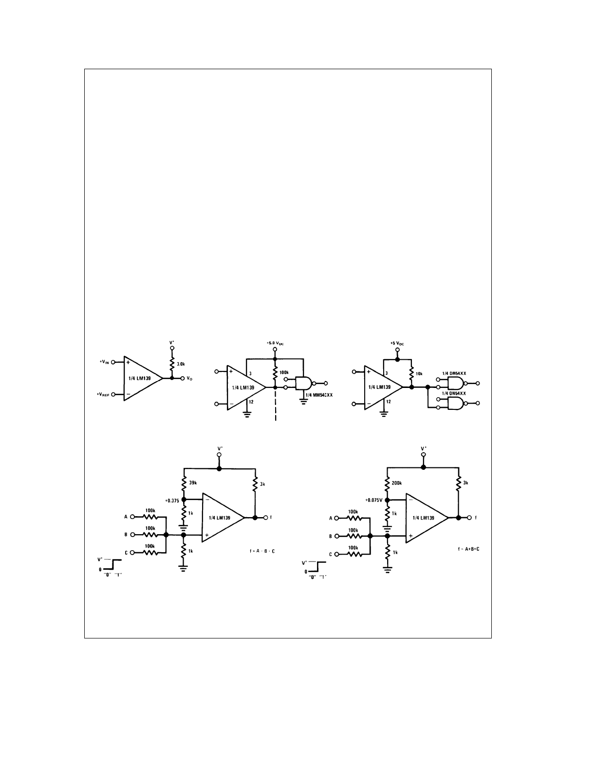
Typical Applications
(V
a
e
5.0 V
DC
)
Basic Comparator
TL/H/5706 – 3
Driving CMOS
TL/H/5706 – 4
Driving TTL
TL/H/5706 – 5
AND Gate
TL/H/5706 – 8
OR Gate
TL/H/5706 – 9
5
Typical Applications
(V
a
e
15 V
DC
) (Continued)
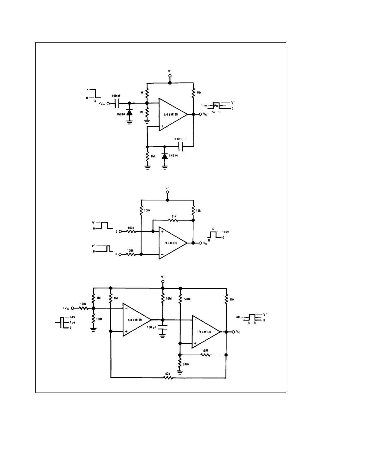
One-Shot Multivibrator
TL/H/5706 – 10
Bi-Stable Multivibrator
TL/H/5706 – 11
One-Shot Multivibrator with Input Lock Out
TL/H/5706 – 12
6
Typical Applications
(V
a
e
15 V
DC
) (Continued)
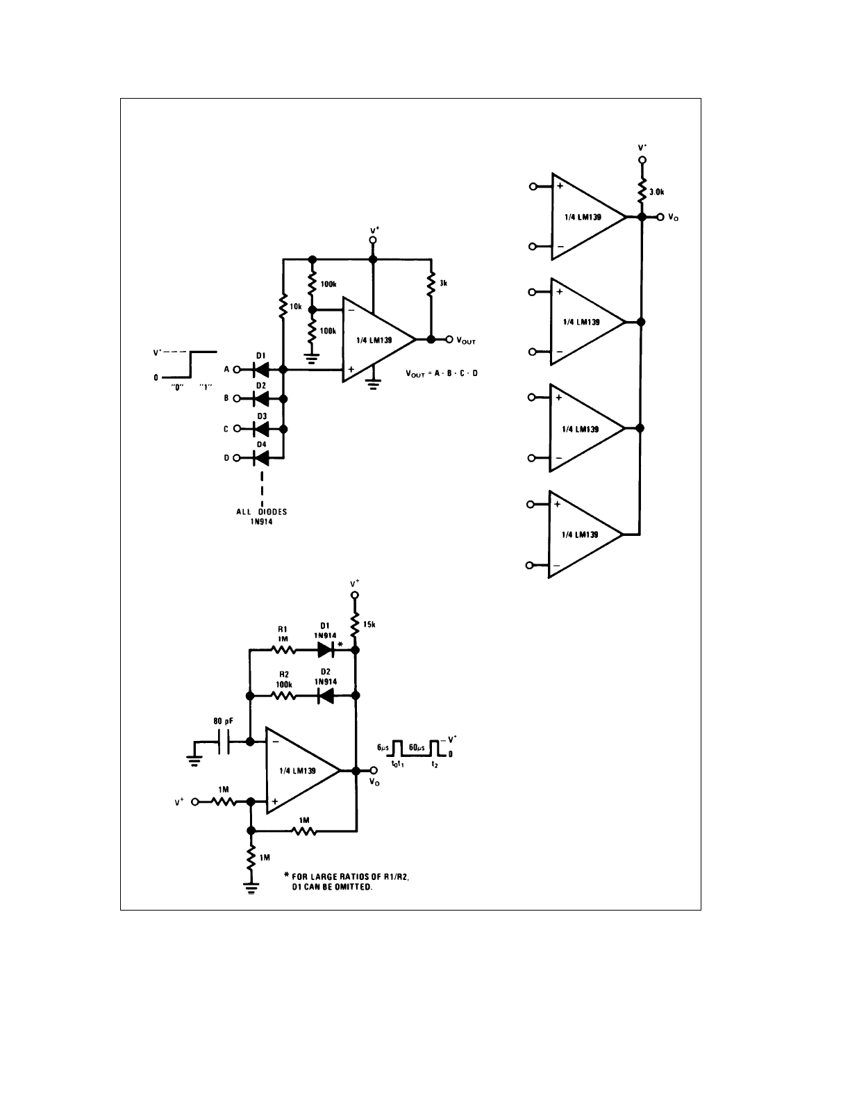
Large Fan-In AND Gate
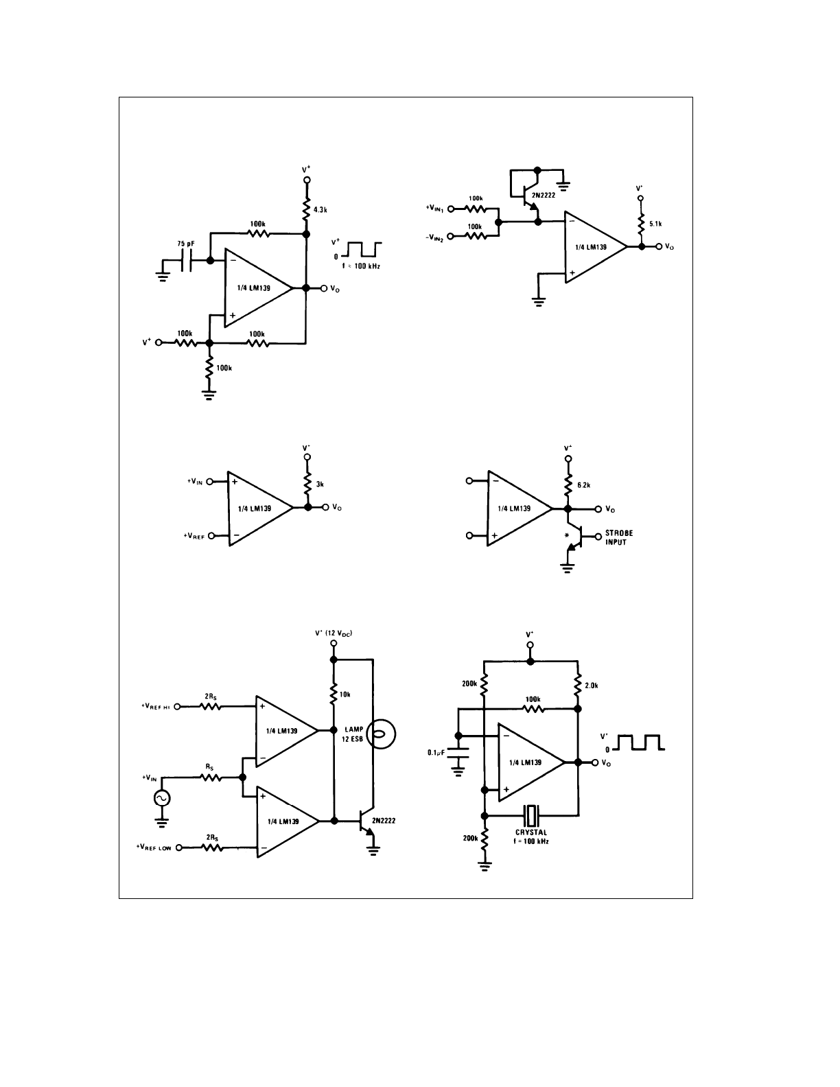
TL/H/5706 – 13
Pulse Generator
TL/H/5706 – 17
ORing the Outputs
TL/H/5706 – 15
7
Typical Applications
(V
a
e
15 V
DC
) (Continued)
Time Delay Generator
TL/H/5706 – 14
Non-Inverting Comparator with Hysteresis
TL/H/5706 – 18
Inverting Comparator with Hysteresis
TL/H/5706 – 19
8
Typical Applications
(V
a
e
15 V
DC
) (Continued)
Squarewave Oscillator
TL/H/5706 – 16
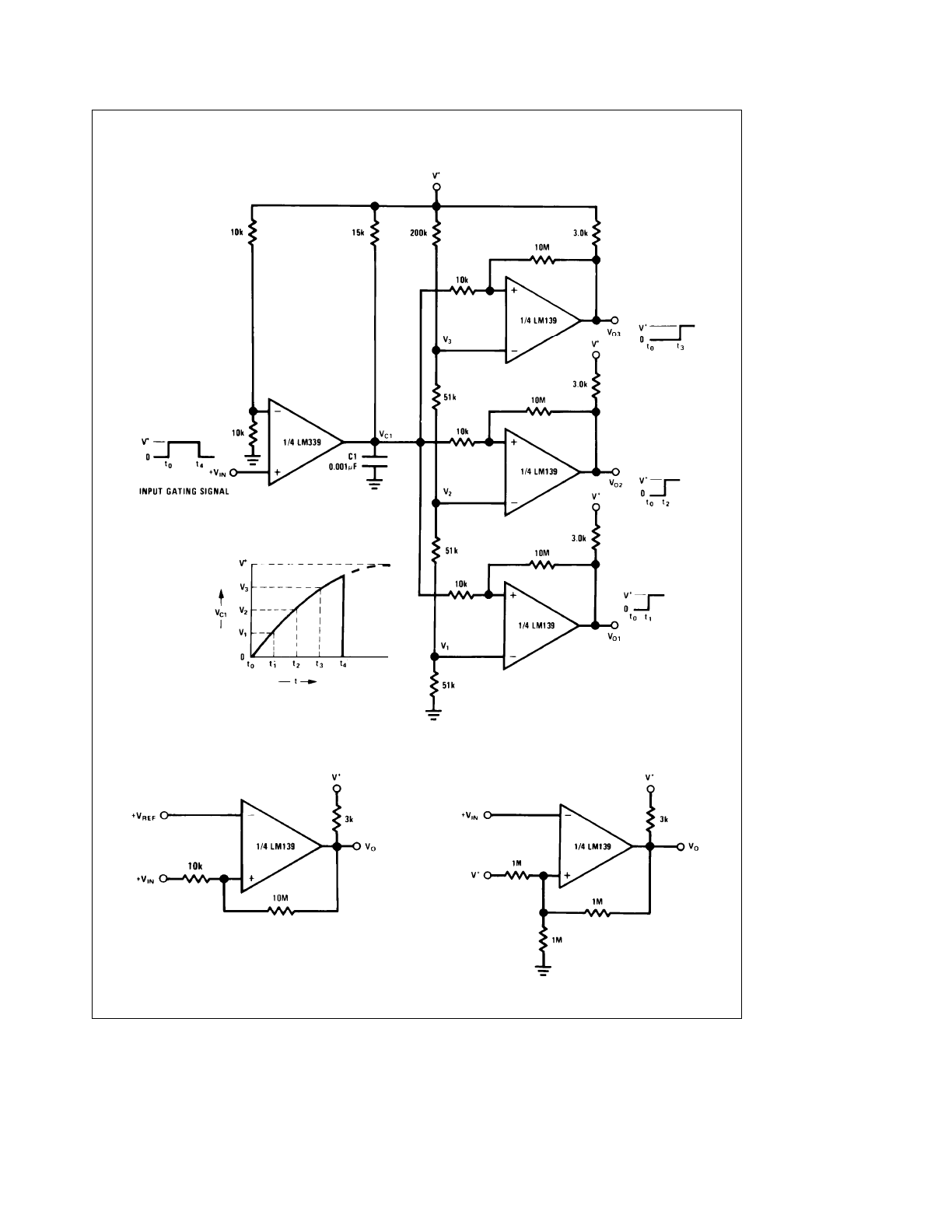
Comparing Input Voltages
of Opposite Polarity
TL/H/5706 – 20
Basic Comparator
TL/H/5706 – 21
Output Strobing
TL/H/5706 – 22
*Or open-collector logic gate without pull-up resistor
Limit Comparator
TL/H/5706 – 24
Crystal Controlled Oscillator
TL/H/5706 – 25
9
Typical Applications
(V
a
e
15 V
DC
) (Continued)
Two-Decade
High-Frequency
VCO
V
a
ea
30
V
DC
a
250
mV
DC
s
V
C
s
a
50
V
DC
700
Hz
s
f
o
s
100
kHz
TL/H/5706
–
2
3
10
Typical Applications
(V
a
e
5 V
DC
) (Continued)
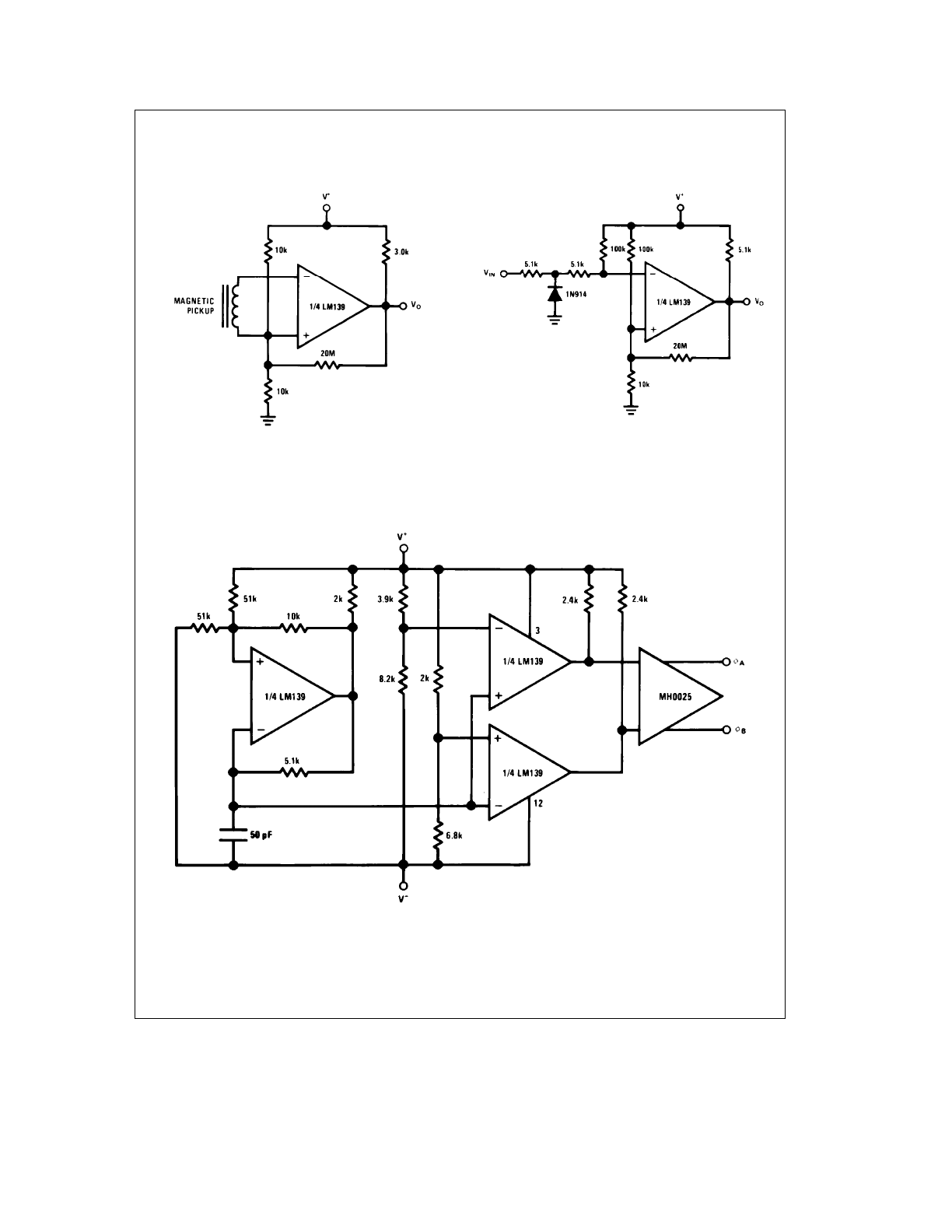
Transducer Amplifier
TL/H/5706 – 28
Zero Crossing Detector (Single Power Supply)
TL/H/5706 – 30
Split-Supply Applications
(V
a
e a
15 V
DC
and V
b
e b
15 V
DC
)
MOS Clock Driver
TL/H/5706 – 31
11
Split-Supply Applications
(V
a
e a
15 V
DC
and V
b
e b
15 V
DC
) (Continued)
Zero Crossing Detector
TL/H/5706 – 32
Comparator With a Negative
Reference
TL/H/5706 – 33
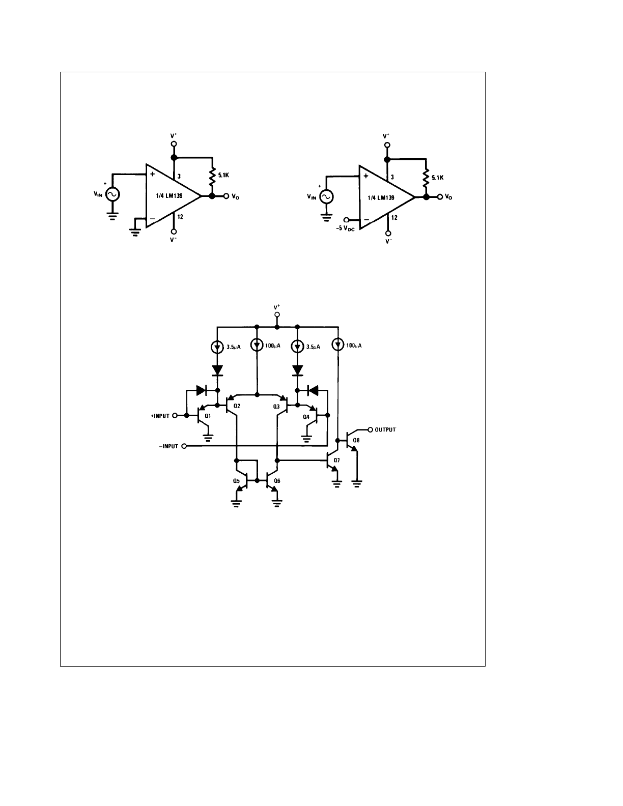
Schematic Diagram
TL/H/5706 – 1
12

13
Physical Dimensions
inches (millimeters)
Order Number LM139AE/883 or LM139E/883
NS Package Number E20A
Ceramic Dual-In-Line Package (J)
Order Number LM139J, LM139J/883, LM139AJ,
LM139AJ/883, LM239J, LM239AJ, LM339J
NS Package Number J14A
14
Physical Dimensions
inches (millimeters) (Continued)
S.O. Package (M)
Order Number LM339AM, LM339M or LM2901M
NS Package Number M14A
Molded Dual-In-Line Package (N)
Order Number LM339N, LM339AN, LM2901N or LM3302N
NS Package Number N14A
15
LM139/LM239/LM339/LM2901/LM3302
Low
Power
Low
Offset
Voltage
Quad
Comparators
Physical Dimensions
inches (millimeters) (Continued)
Order Number LM139AW/883 or LM139W/883
NS Package Number W14B
LIFE SUPPORT POLICY
NATIONAL’S PRODUCTS ARE NOT AUTHORIZED FOR USE AS CRITICAL COMPONENTS IN LIFE SUPPORT
DEVICES OR SYSTEMS WITHOUT THE EXPRESS WRITTEN APPROVAL OF THE PRESIDENT OF NATIONAL
SEMICONDUCTOR CORPORATION. As used herein:
1. Life support devices or systems are devices or
2. A critical component is any component of a life
systems which, (a) are intended for surgical implant
support device or system whose failure to perform can
into the body, or (b) support or sustain life, and whose
be reasonably expected to cause the failure of the life
failure to perform, when properly used in accordance
support device or system, or to affect its safety or
with instructions for use provided in the labeling, can
effectiveness.
be reasonably expected to result in a significant injury
to the user.
National Semiconductor
National Semiconductor
National Semiconductor
National Semiconductor
Corporation
Europe
Hong Kong Ltd.
Japan Ltd.
1111 West Bardin Road
Fax: (
a
49) 0-180-530 85 86
13th Floor, Straight Block,
Tel: 81-043-299-2309
Arlington, TX 76017
Email: cnjwge
@
tevm2.nsc.com
Ocean Centre, 5 Canton Rd.
Fax: 81-043-299-2408
Tel: 1(800) 272-9959
Deutsch Tel: (
a
49) 0-180-530 85 85
Tsimshatsui, Kowloon
Fax: 1(800) 737-7018
English
Tel: (
a
49) 0-180-532 78 32
Hong Kong
Fran
3ais Tel: (
a
49) 0-180-532 93 58
Tel: (852) 2737-1600
Italiano
Tel: (
a
49) 0-180-534 16 80
Fax: (852) 2736-9960
National does not assume any responsibility for use of any circuitry described, no circuit patent licenses are implied and National reserves the right at any time without notice to change said circuitry and specifications.