
LM124/LM224/LM324/LM2902
Low Power Quad Operational Amplifiers
General Description
The LM124 series consists of four independent, high gain,
internally frequency compensated operational amplifiers
which were designed specifically to operate from a single
power supply over a wide range of voltages. Operation from
split power supplies is also possible and the low power sup-
ply current drain is independent of the magnitude of the
power supply voltage.
Application areas include transducer amplifiers, DC gain
blocks and all the conventional op amp circuits which now
can be more easily implemented in single power supply sys-
tems. For example, the LM124 series can be directly oper-
ated off of the standard +5V power supply voltage which is
used in digital systems and will easily provide the required
interface electronics without requiring the additional
±
15V
power supplies.
Unique Characteristics
n
In the linear mode the input common-mode voltage
range includes ground and the output voltage can also
swing to ground, even though operated from only a
single power supply voltage
n
The unity gain cross frequency is temperature
compensated
n
The input bias current is also temperature compensated
Advantages
n
Eliminates need for dual supplies
n
Four internally compensated op amps in a single
package
n
Allows directly sensing near GND and V
OUT
also goes
to GND
n
Compatible with all forms of logic
n
Power drain suitable for battery operation
Features
n
Internally frequency compensated for unity gain
n
Large DC voltage gain
100 dB
n
Wide bandwidth (unity gain)
1 MHz
(temperature compensated)
n
Wide power supply range:
Single supply
3V to 32V
or dual supplies
±
1.5V to
±
16V
n
Very low supply current drain (700 µA) — essentially
independent of supply voltage
n
Low input biasing current
45 nA
(temperature compensated)
n
Low input offset voltage
2 mV
and offset current:
5 nA
n
Input common-mode voltage range includes ground
n
Differential input voltage range equal to the power
supply voltage
n
Large output voltage swing
0V to V
+
− 1.5V
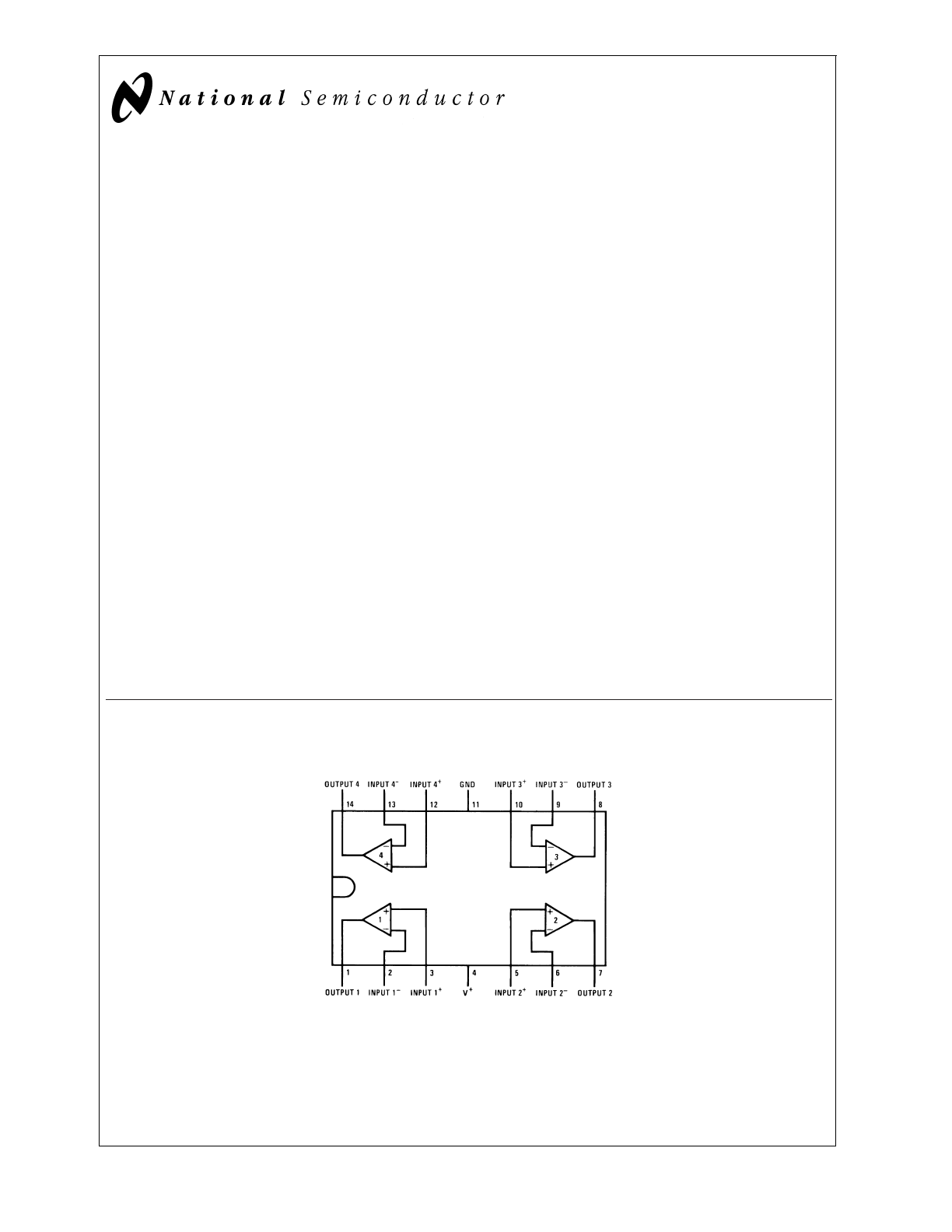
Connection Diagram
Note 1: LM124A available per JM38510/11006
Note 2: LM124 available per JM38510/11005
Dual-In-Line Package
DS009299-1
Top View
Order Number LM124J, LM124AJ, LM124J/883 (Note 2), LM124AJ/883 (Note 1), LM224J,
LM224AJ, LM324J, LM324M, LM324MX, LM324AM, LM324AMX, LM2902M, LM2902MX, LM324N, LM324AN,
LM324MT, LM324MTX or LM2902N LM124AJRQML and LM124AJRQMLV(Note 3)
See NS Package Number J14A, M14A or N14A
August 2000
LM124/LM224/LM324/LM2902
Low
Power
Quad
Operational
Amplifiers
© 2000 National Semiconductor Corporation
DS009299
www.national.com
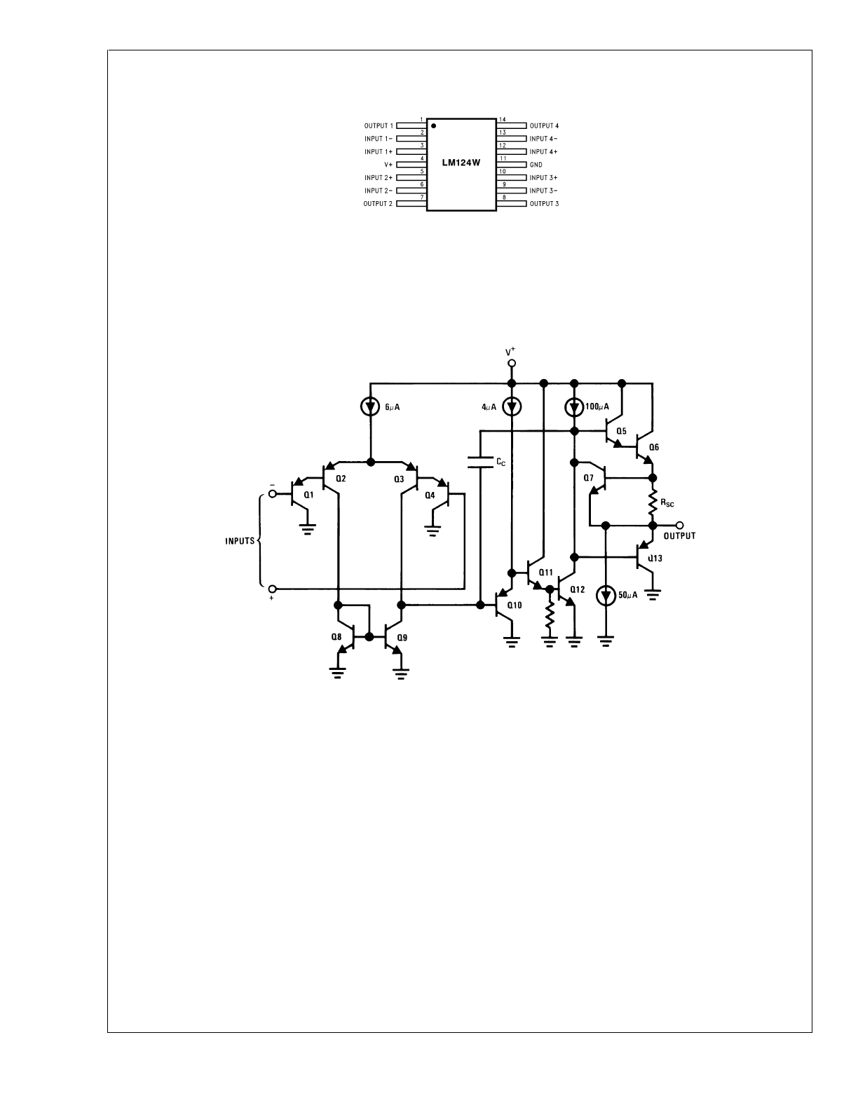
Connection Diagram
(Continued)
Note 3: See STD Mil DWG 5962R99504 for Radiation Tolerant Device
Schematic Diagram
(Each Amplifier)
DS009299-33
Order Number LM124AW/883, LM124AWG/883, LM124W/883 or LM124WG/883
LM124AWRQML and LM124AWRQMLV(Note 3)
See NS Package Number W14B
LM124AWGRQML and LM124AWGRQMLV(Note 3)
See NS Package Number WG14A
DS009299-2
LM124/LM224/LM324/LM2902
www.national.com
2
Absolute Maximum Ratings
(Note 12)
If Military/Aerospace specified devices are required,
please contact the National Semiconductor Sales Office/
Distributors for availability and specifications.
LM124/LM224/LM324
LM2902
LM124A/LM224A/LM324A
Supply Voltage, V
+
32V
26V
Differential Input Voltage
32V
26V
Input Voltage
−0.3V to +32V
−0.3V to +26V
Input Current
(V
IN
<
−0.3V) (Note 6)
50 mA
50 mA
Power Dissipation (Note 4)
Molded DIP
1130 mW
1130 mW
Cavity DIP
1260 mW
1260 mW
Small Outline Package
800 mW
800 mW
Output Short-Circuit to GND
(One Amplifier) (Note 5)
V
+
≤
15V and T
A
= 25˚C
Continuous
Continuous
Operating Temperature Range
−40˚C to +85˚C
LM324/LM324A
0˚C to +70˚C
LM224/LM224A
−25˚C to +85˚C
LM124/LM124A
−55˚C to +125˚C
Storage Temperature Range
−65˚C to +150˚C
−65˚C to +150˚C
Lead Temperature (Soldering, 10 seconds)
260˚C
260˚C
Soldering Information
Dual-In-Line Package
Soldering (10 seconds)
260˚C
260˚C
Small Outline Package
Vapor Phase (60 seconds)
215˚C
215˚C
Infrared (15 seconds)
220˚C
220˚C
See AN-450 “Surface Mounting Methods and Their Effect on Product Reliability” for other methods of soldering surface mount
devices.
ESD Tolerance (Note 13)
250V
250V
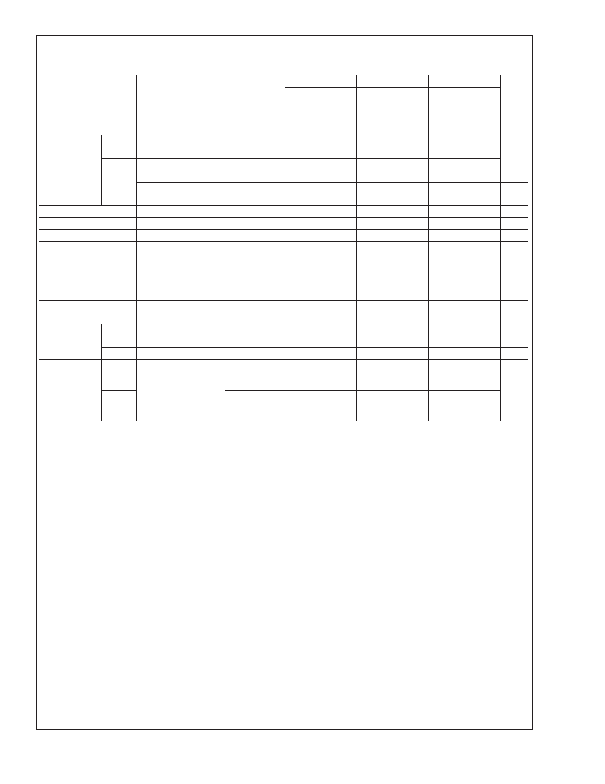
Electrical Characteristics
V
+
= +5.0V, (Note 7), unless otherwise stated
Parameter
Conditions
LM124A
LM224A
LM324A
Units
Min
Typ
Max
Min
Typ
Max
Min
Typ
Max
Input Offset Voltage
(Note 8) T
A
= 25˚C
1
2
1
3
2
3
mV
Input Bias Current
I
IN(+)
or I
IN(−)
, V
CM
= 0V,
20
50
40
80
45
100
nA
(Note 9)
T
A
= 25˚C
Input Offset Current
I
IN(+)
or I
IN(−)
, V
CM
= 0V,
2
10
2
15
5
30
nA
T
A
= 25˚C
Input Common-Mode
V
+
= 30V, (LM2902, V
+
= 26V),
0
V
+
−1.5
0
V
+
−1.5
0
V
+
−1.5
V
Voltage Range (Note 10)
T
A
= 25˚C
Supply Current
Over Full Temperature Range
R
L
=
∞
On All Op Amps
mA
V
+
= 30V (LM2902 V
+
= 26V)
1.5
3
1.5
3
1.5
3
V
+
= 5V
0.7
1.2
0.7
1.2
0.7
1.2
Large Signal
V
+
= 15V, R
L
≥
2k
Ω
,
50
100
50
100
25
100
V/mV
Voltage Gain
(V
O
= 1V to 11V), T
A
= 25˚C
Common-Mode
DC, V
CM
= 0V to V
+
− 1.5V,
70
85
70
85
65
85
dB
Rejection Ratio
T
A
= 25˚C
LM124/LM224/LM324/LM2902
www.national.com
3
Electrical Characteristics
(Continued)
V
+
= +5.0V, (Note 7), unless otherwise stated
Parameter
Conditions
LM124A
LM224A
LM324A
Units
Min
Typ
Max
Min
Typ
Max
Min
Typ
Max
Power Supply
V
+
= 5V to 30V
Rejection Ratio
(LM2902, V
+
= 5V to 26V),
65
100
65
100
65
100
dB
T
A
= 25˚C
Amplifier-to-Amplifier
f = 1 kHz to 20 kHz, T
A
= 25˚C
−120
−120
−120
dB
Coupling (Note 11)
(Input Referred)
Output Current
Source
V
IN
+
= 1V, V
IN
−
= 0V,
20
40
20
40
20
40
V
+
= 15V, V
O
= 2V, T
A
= 25˚C
mA
Sink
V
IN
−
= 1V, V
IN
+
= 0V,
10
20
10
20
10
20
V
+
= 15V, V
O
= 2V, T
A
= 25˚C
V
IN
−
= 1V, V
IN
+
= 0V,
12
50
12
50
12
50
µA
V
+
= 15V, V
O
= 200 mV, T
A
= 25˚C
Short Circuit to Ground
(Note 5) V
+
= 15V, T
A
= 25˚C
40
60
40
60
40
60
mA
Input Offset Voltage
(Note 8)
4
4
5
mV
V
OS
Drift
R
S
= 0
Ω
7
20
7
20
7
30
µV/˚C
Input Offset Current
I
IN(+)
− I
IN(−)
, V
CM
= 0V
30
30
75
nA
I
OS
Drift
R
S
= 0
Ω
10
200
10
200
10
300
pA/˚C
Input Bias Current
I
IN(+)
or I
IN(−)
40
100
40
100
40
200
nA
Input Common-Mode
V
+
= +30V
0
V
+
−2
0
V
+
−2
0
V
+
−2
V
Voltage Range (Note 10)
(LM2902, V
+
= 26V)
Large Signal
V
+
= +15V (V
O
Swing = 1V to 11V)
Voltage Gain
R
L
≥
2 k
Ω
25
25
15
V/mV
Output Voltage
V
OH
V
+
= 30V
R
L
= 2 k
Ω
26
26
26
V
Swing
(LM2902, V
+
= 26V)
R
L
= 10 k
Ω
27
28
27
28
27
28
V
OL
V
+
= 5V, R
L
= 10 k
Ω
5
20
5
20
5
20
mV
Output Current
Source
V
O
= 2V
V
IN
+
= +1V,
10
20
10
20
10
20
V
IN
−
= 0V,
V
+
= 15V
mA
Sink
V
IN
−
= +1V,
10
15
5
8
5
8
V
IN
+
= 0V,
V
+
= 15V
Electrical Characteristics
V
+
= +5.0V, (Note 7), unless otherwise stated
Parameter
Conditions
LM124/LM224
LM324
LM2902
Units
Min
Typ
Max
Min
Typ
Max
Min
Typ
Max
Input Offset Voltage
(Note 8) T
A
= 25˚C
2
5
2
7
2
7
mV
Input Bias Current
I
IN(+)
or I
IN(−)
, V
CM
= 0V,
45
150
45
250
45
250
nA
(Note 9)
T
A
= 25˚C
Input Offset Current
I
IN(+)
or I
IN(−)
, V
CM
= 0V,
3
30
5
50
5
50
nA
T
A
= 25˚C
Input Common-Mode
V
+
= 30V, (LM2902, V
+
= 26V),
0
V
+
−1.5
0
V
+
−1.5
0
V
+
−1.5
V
Voltage Range (Note 10)
T
A
= 25˚C
Supply Current
Over Full Temperature Range
R
L
=
∞
On All Op Amps
mA
V
+
= 30V (LM2902 V
+
= 26V)
1.5
3
1.5
3
1.5
3
V
+
= 5V
0.7
1.2
0.7
1.2
0.7
1.2
Large Signal
V
+
= 15V, R
L
≥
2k
Ω
,
50
100
25
100
25
100
V/mV
Voltage Gain
(V
O
= 1V to 11V), T
A
= 25˚C
Common-Mode
DC, V
CM
= 0V to V
+
− 1.5V,
70
85
65
85
50
70
dB
Rejection Ratio
T
A
= 25˚C
Power Supply
V
+
= 5V to 30V
Rejection Ratio
(LM2902, V
+
= 5V to 26V),
65
100
65
100
50
100
dB
LM124/LM224/LM324/LM2902
www.national.com
4
Electrical Characteristics
(Continued)
V
+
= +5.0V, (Note 7), unless otherwise stated
Parameter
Conditions
LM124/LM224
LM324
LM2902
Units
Min
Typ
Max
Min
Typ
Max
Min
Typ
Max
T
A
= 25˚C
Amplifier-to-Amplifier
f = 1 kHz to 20 kHz, T
A
= 25˚C
−120
−120
−120
dB
Coupling (Note 11)
(Input Referred)
Output Current
Source
V
IN
+
= 1V, V
IN
−
= 0V,
20
40
20
40
20
40
V
+
= 15V, V
O
= 2V, T
A
= 25˚C
mA
Sink
V
IN
−
= 1V, V
IN
+
= 0V,
10
20
10
20
10
20
V
+
= 15V, V
O
= 2V, T
A
= 25˚C
V
IN
−
= 1V, V
IN
+
= 0V,
12
50
12
50
12
50
µA
V
+
= 15V, V
O
= 200 mV, T
A
= 25˚C
Short Circuit to Ground
(Note 5) V
+
= 15V, T
A
= 25˚C
40
60
40
60
40
60
mA
Input Offset Voltage
(Note 8)
7
9
10
mV
V
OS
Drift
R
S
= 0
Ω
7
7
7
µV/˚C
Input Offset Current
I
IN(+)
− I
IN(−)
, V
CM
= 0V
100
150
45
200
nA
I
OS
Drift
R
S
= 0
Ω
10
10
10
pA/˚C
Input Bias Current
I
IN(+)
or I
IN(−)
40
300
40
500
40
500
nA
Input Common-Mode
V
+
= +30V
0
V
+
−2
0
V
+
−2
0
V
+
−2
V
Voltage Range (Note 10)
(LM2902, V
+
= 26V)
Large Signal
V
+
= +15V (V
O
Swing = 1V to 11V)
Voltage Gain
R
L
≥
2 k
Ω
25
15
15
V/mV
Output Voltage
V
OH
V
+
= 30V
R
L
= 2 k
Ω
26
26
22
V
Swing
(LM2902, V
+
= 26V)
R
L
= 10 k
Ω
27
28
27
28
23
24
V
OL
V
+
= 5V, R
L
= 10 k
Ω
5
20
5
20
5
100
mV
Output Current
Source
V
O
= 2V
V
IN
+
= +1V,
10
20
10
20
10
20
V
IN
−
= 0V,
V
+
= 15V
mA
Sink
V
IN
−
= +1V,
5
8
5
8
5
8
V
IN
+
= 0V,
V
+
= 15V
Note 4: For operating at high temperatures, the LM324/LM324A/LM2902 must be derated based on a +125˚C maximum junction temperature and a thermal resis-
tance of 88˚C/W which applies for the device soldered in a printed circuit board, operating in a still air ambient. The LM224/LM224A and LM124/LM124A can be de-
rated based on a +150˚C maximum junction temperature. The dissipation is the total of all four amplifiers — use external resistors, where possible, to allow the am-
plifier to saturate of to reduce the power which is dissipated in the integrated circuit.
Note 5: Short circuits from the output to V
+
can cause excessive heating and eventual destruction. When considering short circuits to ground, the maximum output
current is approximately 40 mA independent of the magnitude of V
+
. At values of supply voltage in excess of +15V, continuous short-circuits can exceed the power
dissipation ratings and cause eventual destruction. Destructive dissipation can result from simultaneous shorts on all amplifiers.
Note 6: This input current will only exist when the voltage at any of the input leads is driven negative. It is due to the collector-base junction of the input PNP tran-
sistors becoming forward biased and thereby acting as input diode clamps. In addition to this diode action, there is also lateral NPN parasitic transistor action on the
IC chip. This transistor action can cause the output voltages of the op amps to go to the V
+
voltage level (or to ground for a large overdrive) for the time duration that
an input is driven negative. This is not destructive and normal output states will re-establish when the input voltage, which was negative, again returns to a value
greater than −0.3V (at 25˚C).
Note 7: These specifications are limited to −55˚C
≤
T
A
≤
+125˚C for the LM124/LM124A. With the LM224/LM224A, all temperature specifications are limited to −25˚C
≤
T
A
≤
+85˚C, the LM324/LM324A temperature specifications are limited to 0˚C
≤
T
A
≤
+70˚C, and the LM2902 specifications are limited to −40˚C
≤
T
A
≤
+85˚C.
Note 8: V
O
.
1.4V, R
S
= 0
Ω
with V
+
from 5V to 30V; and over the full input common-mode range (0V to V
+
− 1.5V) for LM2902, V
+
from 5V to 26V.
Note 9: The direction of the input current is out of the IC due to the PNP input stage. This current is essentially constant, independent of the state of the output so
no loading change exists on the input lines.
Note 10: The input common-mode voltage of either input signal voltage should not be allowed to go negative by more than 0.3V (at 25˚C). The upper end of the
common-mode voltage range is V
+
− 1.5V (at 25˚C), but either or both inputs can go to +32V without damage (+26V for LM2902), independent of the magnitude of
V
+
.
Note 11: Due to proximity of external components, insure that coupling is not originating via stray capacitance between these external parts. This typically can be
detected as this type of capacitance increases at higher frequencies.
Note 12: Refer to RETS124AX for LM124A military specifications and refer to RETS124X for LM124 military specifications.
Note 13: Human body model, 1.5 k
Ω
in series with 100 pF.
LM124/LM224/LM324/LM2902
www.national.com
5
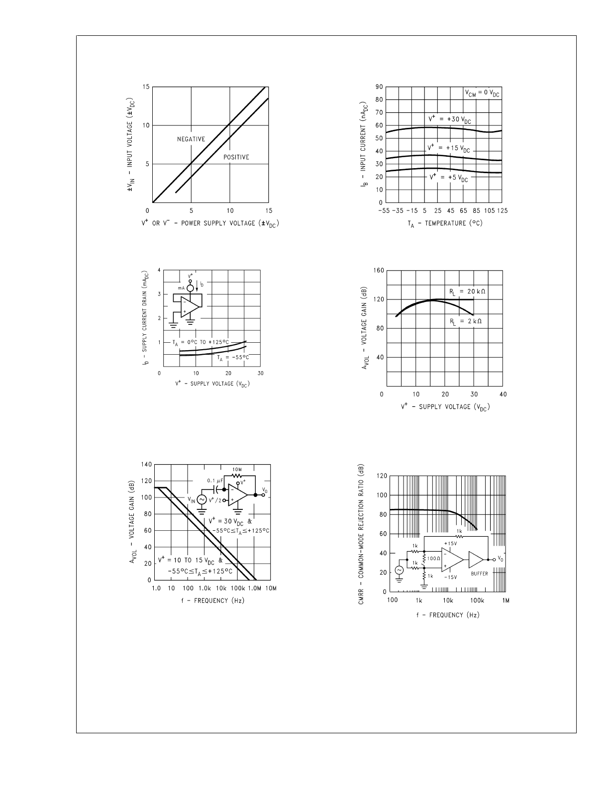
Typical Performance Characteristics
Input Voltage Range
DS009299-34
Input Current
DS009299-35
Supply Current
DS009299-36
Voltage Gain
DS009299-37
Open Loop Frequency
Response
DS009299-38
Common Mode Rejection
Ratio
DS009299-39
LM124/LM224/LM324/LM2902
www.national.com
6
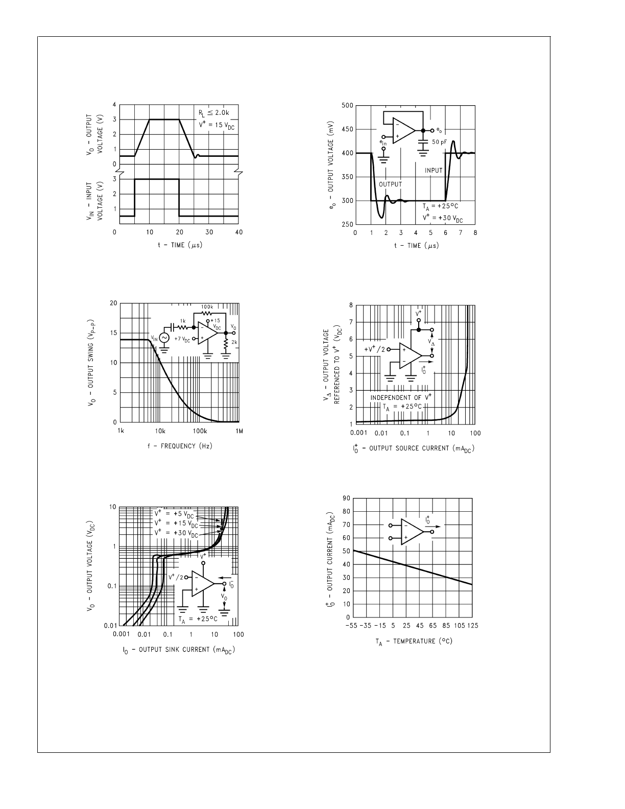
Typical Performance Characteristics
(Continued)
Voltage Follower Pulse
Response
DS009299-40
Voltage Follower Pulse
Response (Small Signal)
DS009299-41
Large Signal Frequency
Response
DS009299-42
Output Characteristics
Current Sourcing
DS009299-43
Output Characteristics
Current Sinking
DS009299-44
Current Limiting
DS009299-45
LM124/LM224/LM324/LM2902
www.national.com
7
Typical Performance Characteristics
(Continued)
Application Hints
The LM124 series are op amps which operate with only a
single power supply voltage, have true-differential inputs,
and remain in the linear mode with an input common-mode
voltage of 0 V
DC
. These amplifiers operate over a wide range
of power supply voltage with little change in performance
characteristics. At 25˚C amplifier operation is possible down
to a minimum supply voltage of 2.3 V
DC
.
The pinouts of the package have been designed to simplify
PC board layouts. Inverting inputs are adjacent to outputs for
all of the amplifiers and the outputs have also been placed at
the corners of the package (pins 1, 7, 8, and 14).
Precautions should be taken to insure that the power supply
for the integrated circuit never becomes reversed in polarity
or that the unit is not inadvertently installed backwards in a
test socket as an unlimited current surge through the result-
ing forward diode within the IC could cause fusing of the in-
ternal conductors and result in a destroyed unit.
Large differential input voltages can be easily accommo-
dated and, as input differential voltage protection diodes are
not needed, no large input currents result from large differen-
tial input voltages. The differential input voltage may be
larger than V
+
without damaging the device. Protection
should be provided to prevent the input voltages from going
negative more than −0.3 V
DC
(at 25˚C). An input clamp diode
with a resistor to the IC input terminal can be used.
To reduce the power supply drain, the amplifiers have a
class A output stage for small signal levels which converts to
class B in a large signal mode. This allows the amplifiers to
both source and sink large output currents. Therefore both
NPN and PNP external current boost transistors can be used
to extend the power capability of the basic amplifiers. The
output voltage needs to raise approximately 1 diode drop
above ground to bias the on-chip vertical PNP transistor for
output current sinking applications.
For ac applications, where the load is capacitively coupled to
the output of the amplifier, a resistor should be used, from
the output of the amplifier to ground to increase the class A
bias current and prevent crossover distortion.
Where the load is directly coupled, as in dc applications,
there is no crossover distortion.
Capacitive loads which are applied directly to the output of
the amplifier reduce the loop stability margin. Values of
50 pF
can
be
accommodated
using
the
worst-case
non-inverting unity gain connection. Large closed loop gains
or resistive isolation should be used if larger load capaci-
tance must be driven by the amplifier.
The bias network of the LM124 establishes a drain current
which is independent of the magnitude of the power supply
voltage over the range of from 3 V
DC
to 30 V
DC
.
Output short circuits either to ground or to the positive power
supply should be of short time duration. Units can be de-
stroyed, not as a result of the short circuit current causing
metal fusing, but rather due to the large increase in IC chip
dissipation which will cause eventual failure due to exces-
sive junction temperatures. Putting direct short-circuits on
more than one amplifier at a time will increase the total IC
power dissipation to destructive levels, if not properly pro-
tected with external dissipation limiting resistors in series
with the output leads of the amplifiers. The larger value of
output source current which is available at 25˚C provides a
larger output current capability at elevated temperatures
(see typical performance characteristics) than a standard IC
op amp.
The circuits presented in the section on typical applications
emphasize operation on only a single power supply voltage.
If complementary power supplies are available, all of the
standard op amp circuits can be used. In general, introduc-
ing a pseudo-ground (a bias voltage reference of V
+
/2) will
allow operation above and below this value in single power
supply systems. Many application circuits are shown which
take advantage of the wide input common-mode voltage
range which includes ground. In most cases, input biasing is
not required and input voltages which range to ground can
easily be accommodated.
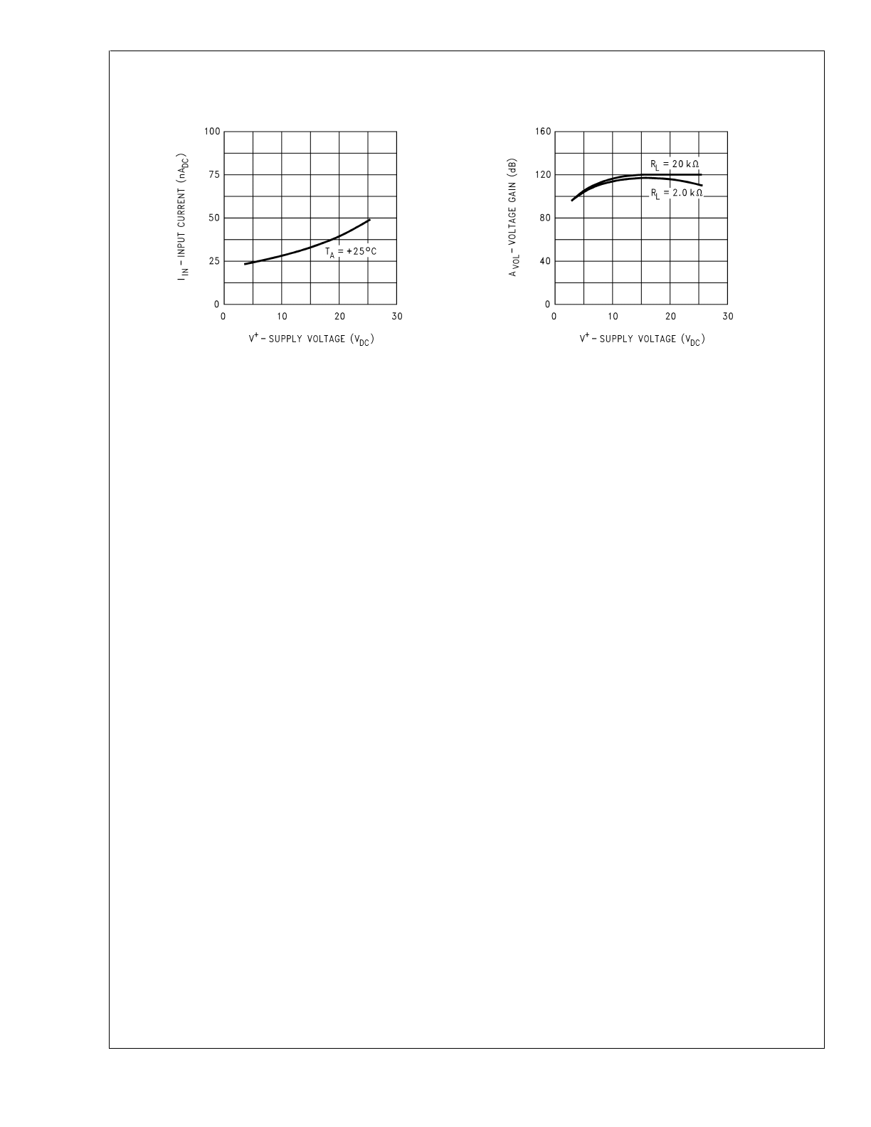
Input Current (LM2902 only)
DS009299-46
Voltage Gain (LM2902 only)
DS009299-47
LM124/LM224/LM324/LM2902
www.national.com
8
Typical Single-Supply Applications
(V
+
= 5.0 V
DC
)
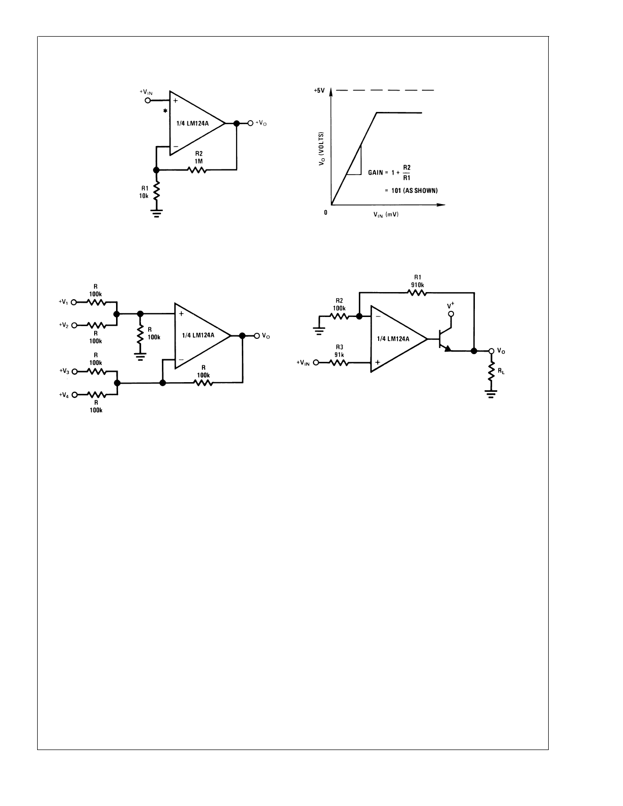
Non-Inverting DC Gain (0V Input = 0V Output)
DS009299-5
*
R not needed due to temperature independent I
IN
DC Summing Amplifier
(V
IN’S
≥
0 V
DC
and V
O
≥
V
DC
)
DS009299-6
Where: V
0
= V
1
+ V
2
− V
3
− V
4
(V
1
+ V
2
)
≥
(V
3
+ V
4
) to keep V
O
>
0 V
DC
Power Amplifier
DS009299-7
V
0
= 0 V
DC
for V
IN
= 0 V
DC
A
V
= 10
LM124/LM224/LM324/LM2902
www.national.com
9
Typical Single-Supply Applications
(V
+
= 5.0 V
DC
) (Continued)
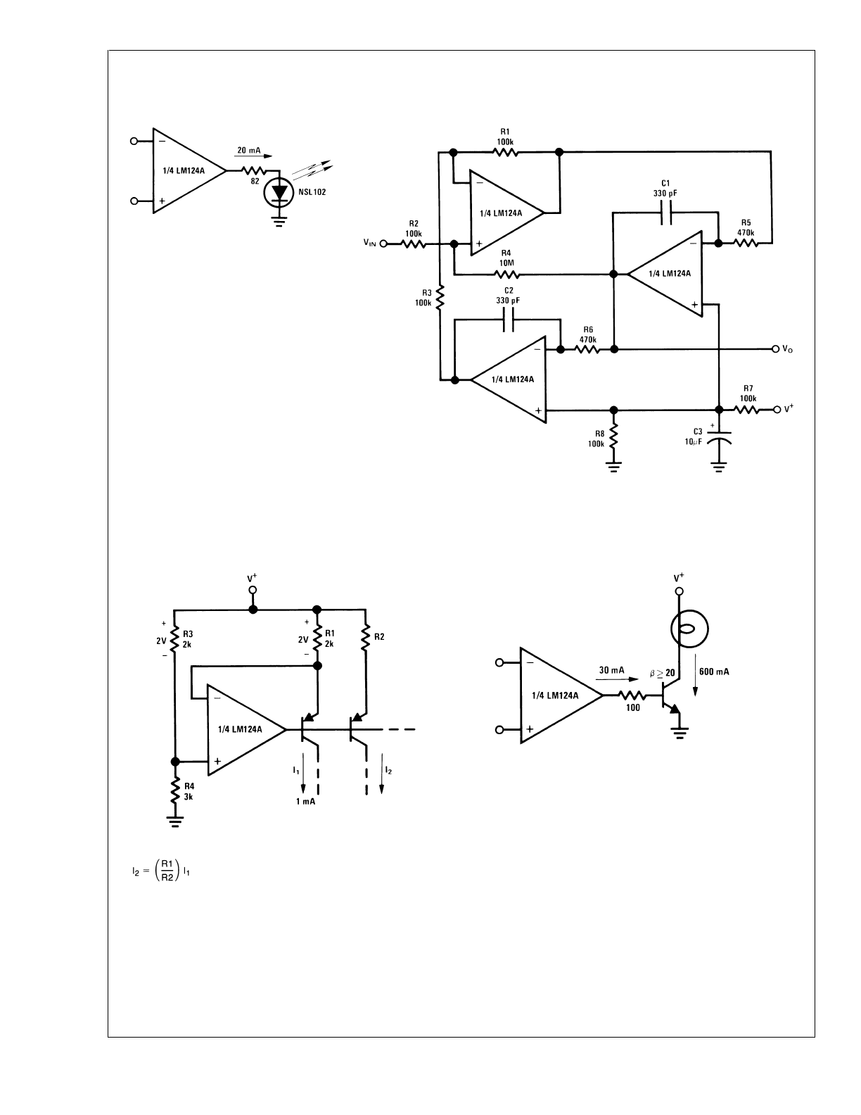
LED Driver
DS009299-8
“BI-QUAD” RC Active Bandpass Filter
DS009299-9
f
o
= 1 kHz
Q = 50
A
V
= 100 (40 dB)
Fixed Current Sources
DS009299-10
Lamp Driver
DS009299-11
LM124/LM224/LM324/LM2902
www.national.com
10
Typical Single-Supply Applications
(V
+
= 5.0 V
DC
) (Continued)
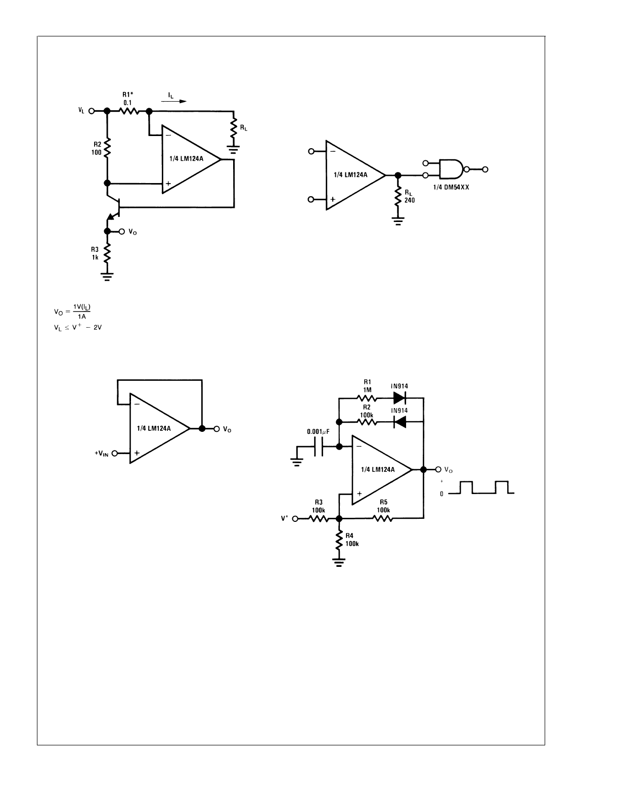
Current Monitor
DS009299-12
*
(Increase R1 for I
L
small)
Driving TTL
DS009299-13
Voltage Follower
DS009299-14
Pulse Generator
DS009299-15
LM124/LM224/LM324/LM2902
www.national.com
11
Typical Single-Supply Applications
(V
+
= 5.0 V
DC
) (Continued)
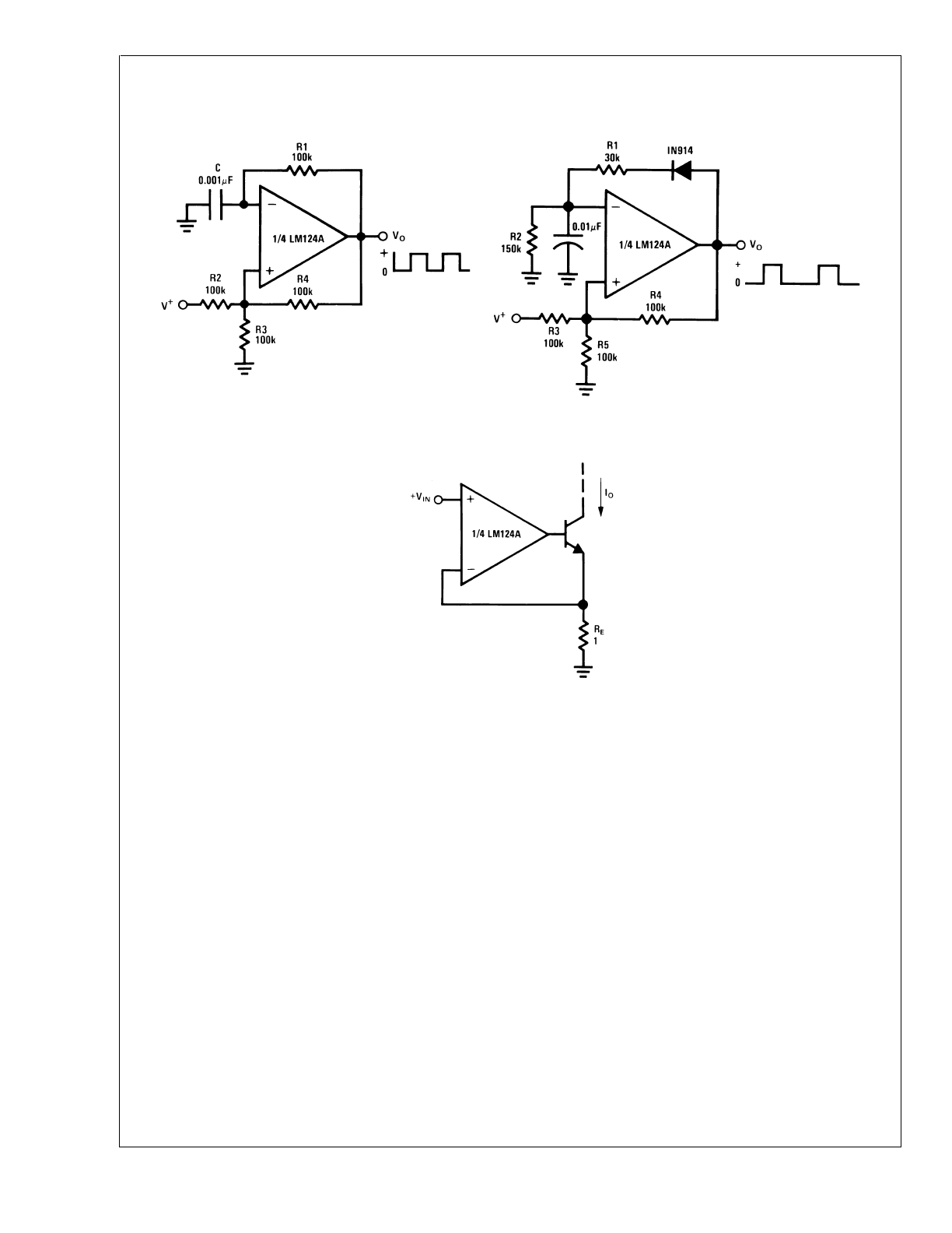
Squarewave Oscillator
DS009299-16
Pulse Generator
DS009299-17
High Compliance Current Sink
DS009299-18
I
O
= 1 amp/volt V
IN
(Increase R
E
for I
o
small)
LM124/LM224/LM324/LM2902
www.national.com
12
Typical Single-Supply Applications
(V
+
= 5.0 V
DC
) (Continued)
Low Drift Peak Detector
DS009299-19
Comparator with Hysteresis
DS009299-20
Ground Referencing a Differential Input Signal
DS009299-21
V
O
= V
R
LM124/LM224/LM324/LM2902
www.national.com
13
Typical Single-Supply Applications
(V
+
= 5.0 V
DC
) (Continued)
Voltage Controlled Oscillator Circuit
DS009299-22
*
Wide control voltage range: 0 V
DC
≤
V
C
≤
2 (V
+
−1.5 V
DC
)
Photo Voltaic-Cell Amplifier
DS009299-23
AC Coupled Inverting Amplifier
DS009299-24
LM124/LM224/LM324/LM2902
www.national.com
14
Typical Single-Supply Applications
(V
+
= 5.0 V
DC
) (Continued)
AC Coupled Non-Inverting Amplifier
DS009299-25
DC Coupled Low-Pass RC Active Filter
DS009299-26
f
O
= 1 kHz
Q = 1
A
V
= 2
LM124/LM224/LM324/LM2902
www.national.com
15
Typical Single-Supply Applications
(V
+
= 5.0 V
DC
) (Continued)
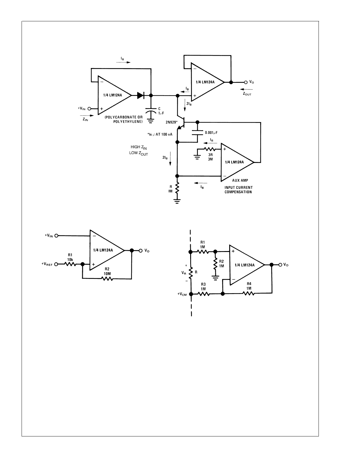
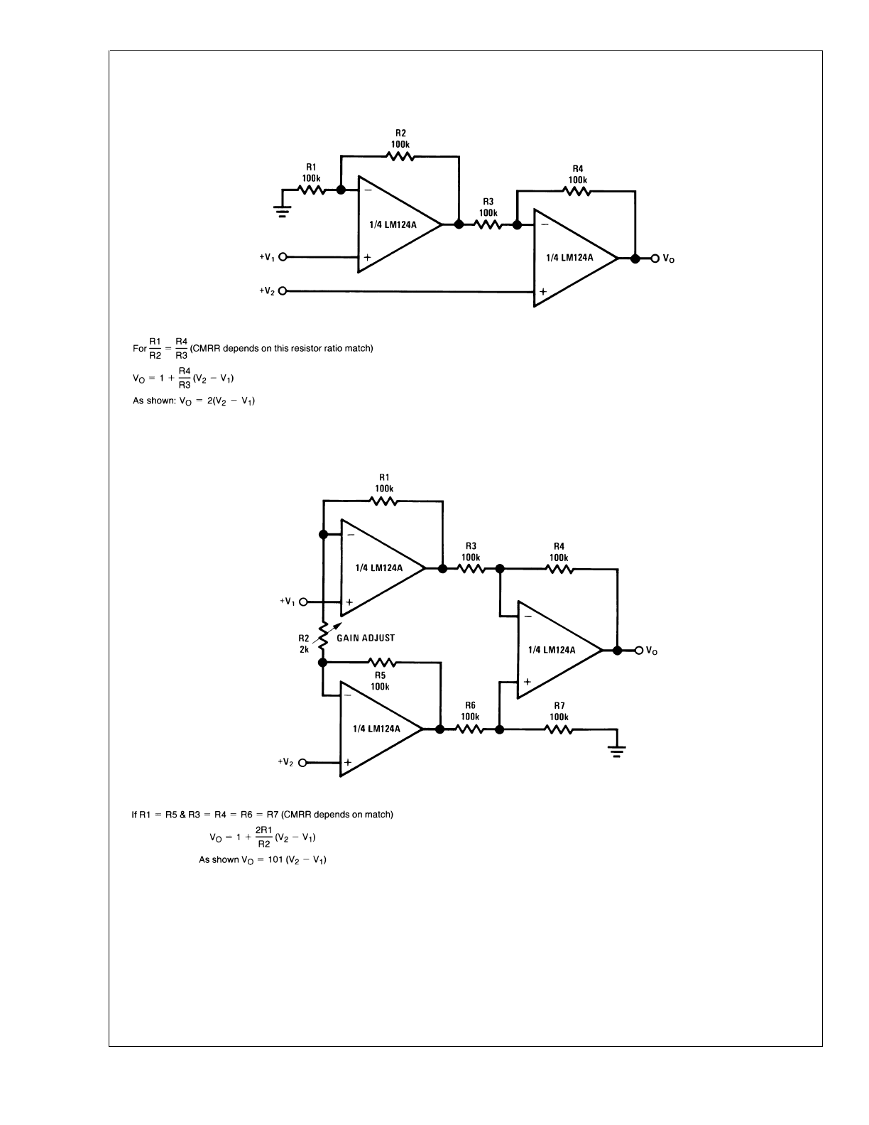
High Input Z, DC Differential Amplifier
DS009299-27
High Input Z Adjustable-Gain
DC Instrumentation Amplifier
DS009299-28
LM124/LM224/LM324/LM2902
www.national.com
16
Typical Single-Supply Applications
(V
+
= 5.0 V
DC
) (Continued)
Using Symmetrical Amplifiers to
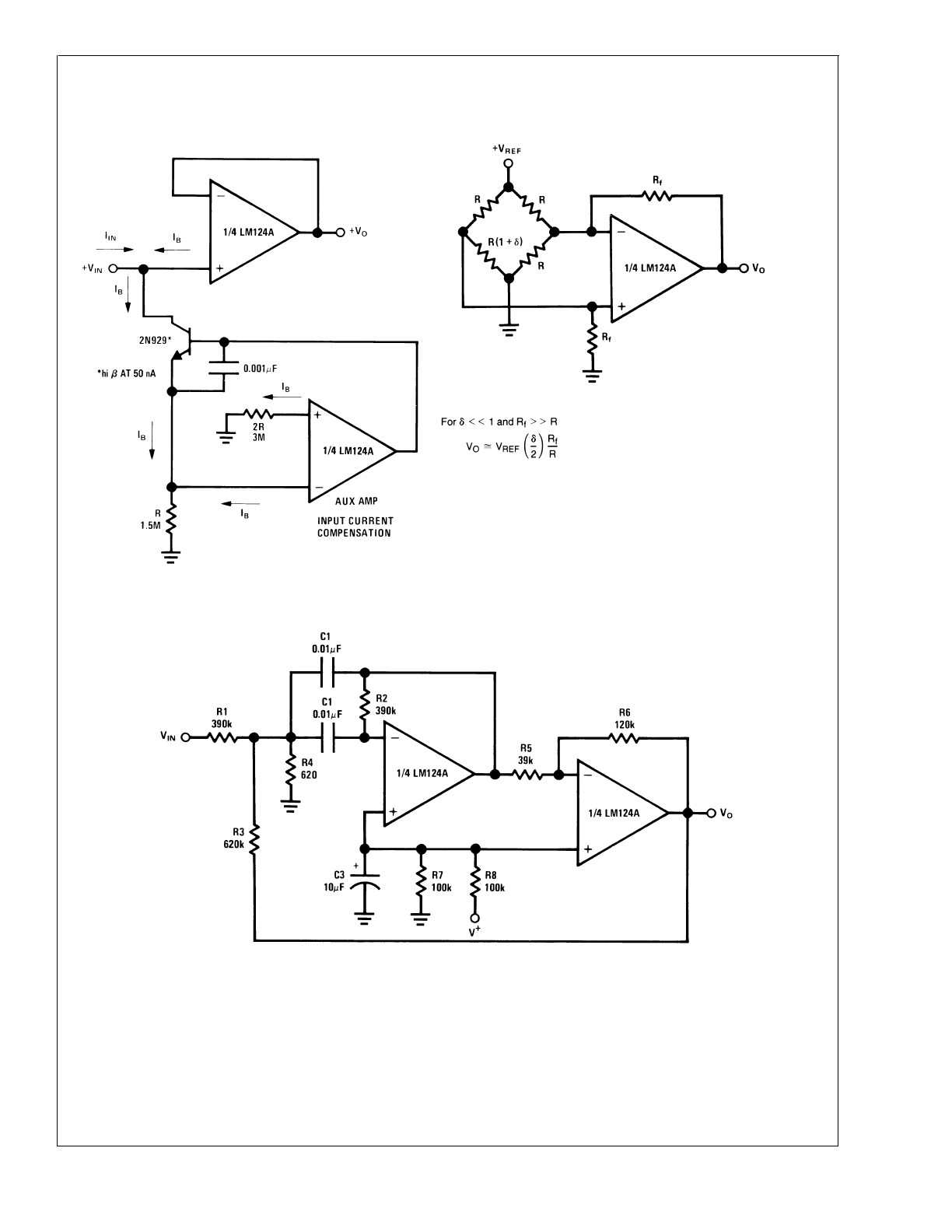
Reduce Input Current (General Concept)
DS009299-29
Bridge Current Amplifier
DS009299-30
Bandpass Active Filter
DS009299-31
f
O
= 1 kHz
Q = 25
LM124/LM224/LM324/LM2902
www.national.com
17
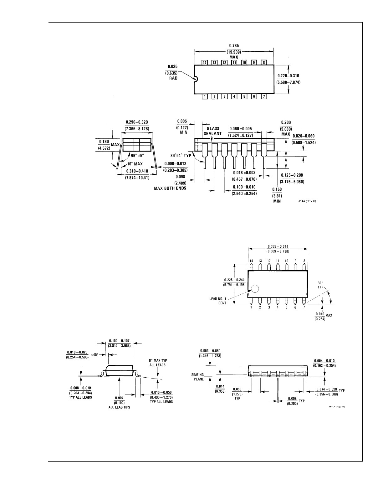
Physical Dimensions
inches (millimeters) unless otherwise noted
Ceramic Dual-In-Line Package (J)
Order Number JL124ABCA, JL124BCA, JL124ASCA, JL124SCA, LM124J,
LM124AJ, LM124AJ/883, LM124J/883, LM224J, LM224AJ or LM324J
NS Package Number J14A
MX S.O. Package (M)
Order Number LM324M, LM324MX, LM324AM, LM324AMX, LM2902M or LM2902MX
NS Package Number M14A
LM124/LM224/LM324/LM2902
www.national.com
18
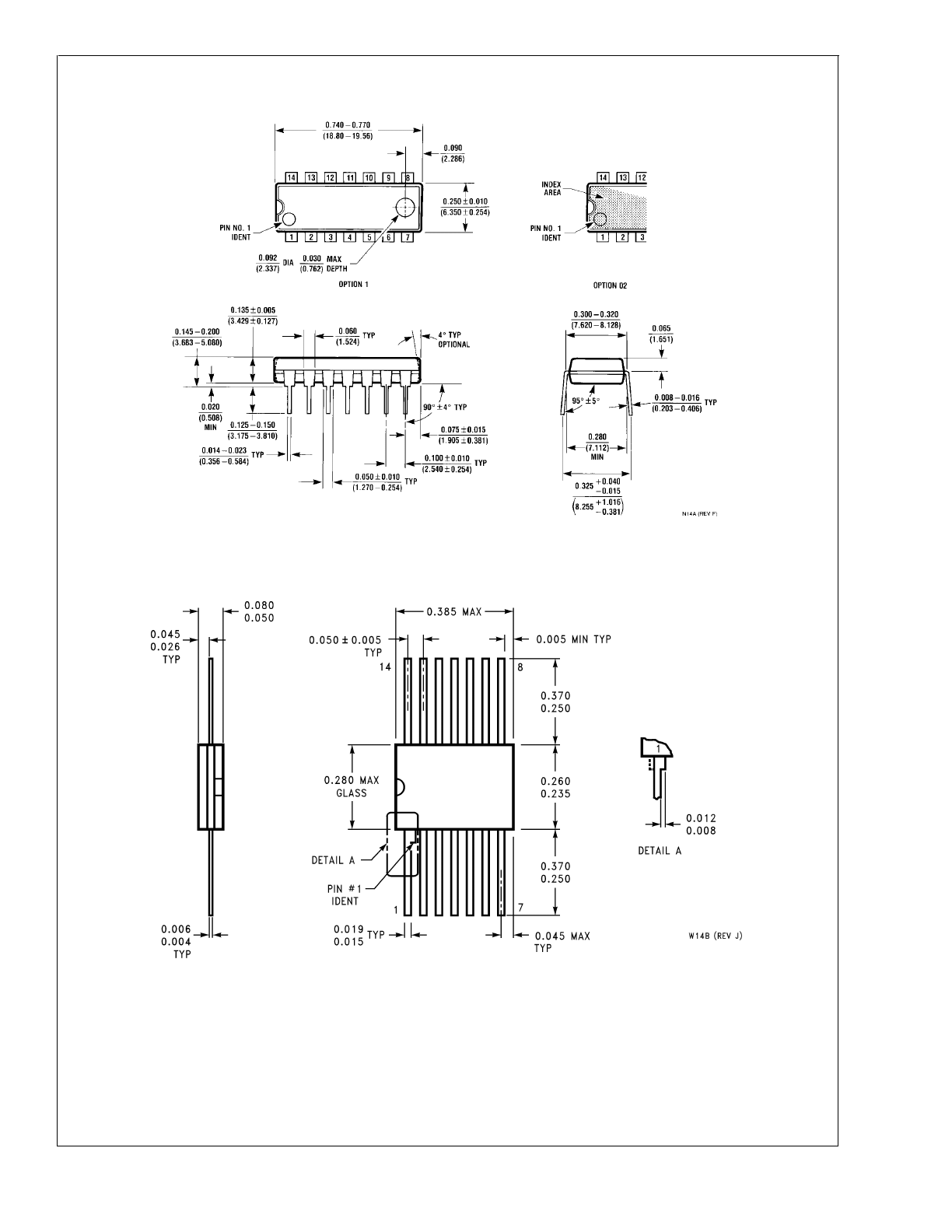
Physical Dimensions
inches (millimeters) unless otherwise noted (Continued)
Molded Dual-In-Line Package (N)
Order Number LM324N, LM324AN or LM2902N
NS Package Number N14A
Ceramic Flatpak Package
Order Number JL124ABDA, JL124ABZA, JL124ASDA, JL124BDA, JL124BZA,
JL124SDA, LM124AW/883, LM124AWG/883, LM124W/883 or LM124WG/883
NS Package Number W14B
LM124/LM224/LM324/LM2902
www.national.com
19
Physical Dimensions
inches (millimeters) unless otherwise noted (Continued)
LIFE SUPPORT POLICY
NATIONAL’S PRODUCTS ARE NOT AUTHORIZED FOR USE AS CRITICAL COMPONENTS IN LIFE SUPPORT
DEVICES OR SYSTEMS WITHOUT THE EXPRESS WRITTEN APPROVAL OF THE PRESIDENT AND GENERAL
COUNSEL OF NATIONAL SEMICONDUCTOR CORPORATION. As used herein:
1. Life support devices or systems are devices or
systems which, (a) are intended for surgical implant
into the body, or (b) support or sustain life, and
whose failure to perform when properly used in
accordance with instructions for use provided in the
labeling, can be reasonably expected to result in a
significant injury to the user.
2. A critical component is any component of a life
support device or system whose failure to perform
can be reasonably expected to cause the failure of
the life support device or system, or to affect its
safety or effectiveness.
National Semiconductor
Corporation
Americas
Tel: 1-800-272-9959
Fax: 1-800-737-7018
Email: support@nsc.com
National Semiconductor
Europe
Fax: +49 (0) 180-530 85 86
Email: europe.support@nsc.com
Deutsch Tel: +49 (0) 69 9508 6208
English
Tel: +44 (0) 870 24 0 2171
Français Tel: +33 (0) 1 41 91 8790
National Semiconductor
Asia Pacific Customer
Response Group
Tel: 65-2544466
Fax: 65-2504466
Email: ap.support@nsc.com
National Semiconductor
Japan Ltd.
Tel: 81-3-5639-7560
Fax: 81-3-5639-7507
www.national.com
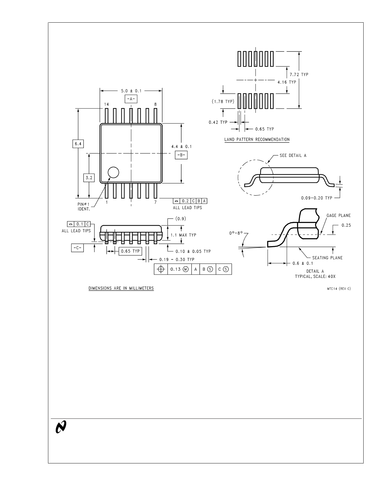
14-Pin TSSOP
Order NumberLM324MT or LM324MTX
NS Package Number MTC14
LM124/LM224/LM324/LM2902
Low
Power
Quad
Operational
Amplifiers
National does not assume any responsibility for use of any circuitry described, no circuit patent licenses are implied and National reserves the right at any time without notice to change said circuitry and specifications.