
LM119/LM219/LM319
High Speed Dual Comparator
General Description
The LM119 series are precision high speed dual compara-
tors fabricated on a single monolithic chip. They are de-
signed to operate over a wide range of supply voltages down
to a single 5V logic supply and ground. Further, they have
higher gain and lower input currents than devices like the
LM710. The uncommitted collector of the output stage
makes the LM119 compatible with RTL, DTL and TTL as well
as capable of driving lamps and relays at currents up to 25
mA.
The LM319A offers improved precision over the standard
LM319, with tighter tolerances on offset voltage, offset cur-
rent, and voltage gain.
Although designed primarily for applications requiring opera-
tion from digital logic supplies, the LM119 series are fully
specified for power supplies up to
±
15V. It features faster re-
sponse than the LM111 at the expense of higher power dis-
sipation. However, the high speed, wide operating voltage
range and low package count make the LM119 much more
versatile than older devices like the LM711.
The LM119 is specified from −55˚C to +125˚C, the LM219 is
specified from −25˚C to +85˚C, and the LM319A and LM319
are specified from 0˚C to +70˚C.
Features
n
Two independent comparators
n
Operates from a single 5V supply
n
Typically 80 ns response time at
±
15V
n
Minimum fan-out of 2 each side
n
Maximum input current of 1 µA over temperature
n
Inputs and outputs can be isolated from system ground
n
High common mode slew rate
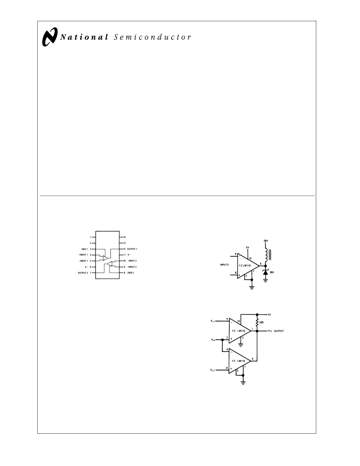
Connection Diagram
Note 1: Also available per SMD# 8601401 or JM38510/10306
Typical Applications
(Note 2)
Dual-In-Line Package
DS005705-4
Top View
Order Number LM119J, LM119J/883 (Note 1),
LM219J, LM319J, LM319AM,
LM319M, LM319AN or LM319N
See NS Package Number J14A, M14A or N14A
Relay Driver
DS005705-5
Note 2: Pin numbers are for metal can package.
Window Detector
DS005705-6
V
OUT
= 5V for V
LT
≤
V
IN
≤
V
UT
V
OUT
= 0 for V
IN
≤
V
LT
or V
IN
≥
V
UT
August 2000
LM1
19/LM219/LM319
High
Speed
Dual
Comparator
© 2000 National Semiconductor Corporation
DS005705
www.national.com
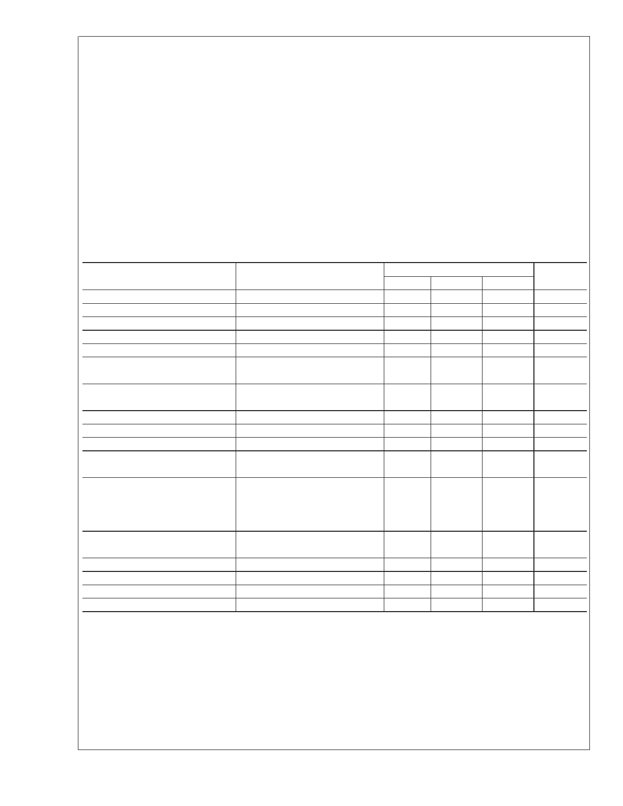
Absolute Maximum Ratings
(Note 9)
If Military/Aerospace specified devices are required,
please contact the National Semiconductor Sales Office/
Distributors for availability and specifications.
Total Supply Voltage
36V
Output to Negative Supply Voltage
36V
Ground to Negative Supply Voltage
25V
Ground to Positive Supply Voltage
18V
Differential Input Voltage
±
5V
Input Voltage (Note 3)
±
15V
ESD rating (1.5 k
Ω
in series with
100 pF)
800V
Power Dissipation (Note 4)
500 mW
Output Short Circuit Duration
10 sec
Storage Temperature Range
−65˚C to 150˚C
Lead Temperature
(Soldering, 10 sec.)
260˚C
Soldering Information
Dual-In-Line Package
Soldering (10 seconds)
260˚C
Small Outline Package
Vapor Phase (60 seconds)
215˚C
Infrared (15 seconds)
220˚C
See AN-450 “Surface Mounting Methods and Their Effect
on Product Reliability” for other methods of soldering
surface mount devices.
Operating Temperature Range
LM119
−55˚C to 125˚C
LM219
−25˚C to 85˚C
Electrical Characteristics
(Note 5)
Parameter
Conditions
LM119/LM219
Units
Min
Typ
Max
Input Offset Voltage (Note 6)
T
A
= 25˚C, R
S
≤
5k
0.7
4.0
mV
Input Offset Current (Note 6)
T
A
= 25˚C
30
75
nA
Input Bias Current
T
A
= 25˚C
150
500
nA
Voltage Gain
T
A
= 25˚C (Note 8)
10
40
V/mV
Response Time (Note 7)
T
A
= 25˚C, V
S
=
±
15V
80
ns
Saturation Voltage
V
IN
≤
−5 mV, I
OUT
= 25 mA
T
A
= 25˚C
0.75
1.5
V
Output Leakage Current
V
IN
≥
5 mV, V
OUT
= 35V
T
A
= 25˚C
0.2
2
µA
Input Offset Voltage (Note 6)
R
S
≤
5k
7
mV
Input Offset Current (Note 6)
100
nA
Input Bias Current
1000
nA
Input Voltage Range
V
S
=
±
15V
−12
±
13
+12
V
V
+
= 5V, V
−
= 0
1
3
V
Saturation Voltage
V
+
≥
4.5V, V
−
= 0
V
IN
≤
−6 mV, I
SINK
≤
3.2 mA
T
A
≥
0˚C
0.23
0.4
V
T
A
≤
0˚C
0.6
V
Output Leakage Current
V
IN
≥
5 mV, V
OUT
= 35V,
1
10
µA
V
−
= V
GND
= 0V
Differential Input Voltage
±
5
V
Positive Supply Current
T
A
= 25˚C, V
+
= 5V, V
−
= 0
4.3
mA
Positive Supply Current
T
A
= 25˚C, V
S
=
±
15V
8
11.5
mA
Negative Supply Current
T
A
= 25˚C, V
S
=
±
15V
3
4.5
mA
Note 3: For supply voltages less than
±
15V the absolute maximum input voltage is equal to the supply voltage.
Note 4: The maximum junction temperature of the LM119 is 150˚C, while that of the LM219 is 110˚C. For operating at elevated temperatures, devices in the H10
package must be derated based on a thermal resistance of 160˚C/W, junction to ambient, or 19˚C/W, junction to case. The thermal resistance of the J14 and N14
packages is 100˚C/W, junction to ambient.
Note 5: These specifications apply for V
S
=
±
15V, and the Ground pin at ground, and −55˚C
≤
T
A
≤
+125˚C, unless otherwise stated. With the LM219, however, all
temperature specifications are limited to −25˚C
≤
T
A
≤
+85˚C. The offset voltage, offset current and bias current specifications apply for any supply voltage from a
single 5V supply up to
±
15V supplies. Do not operate the device with more than 16V from ground to V
S
.
Note 6: The offset voltages and offset currents given are the maximum values required to drive the output within a volt of either supply with a 1 mA load. Thus, these
parameters define an error band and take into account the worst case effects of voltage gain and input impedance.
Note 7: The response time specified (see definitions) is for a 100 mV input step with 5 mV overdrive.
Note 8: Output is pulled up to 15V through a 1.4 k
Ω
resistor.
Note 9: Refer to RETS119X for LM119H/883 and LM119J/883 specifications.
LM1
19/LM219/LM319
www.national.com
2
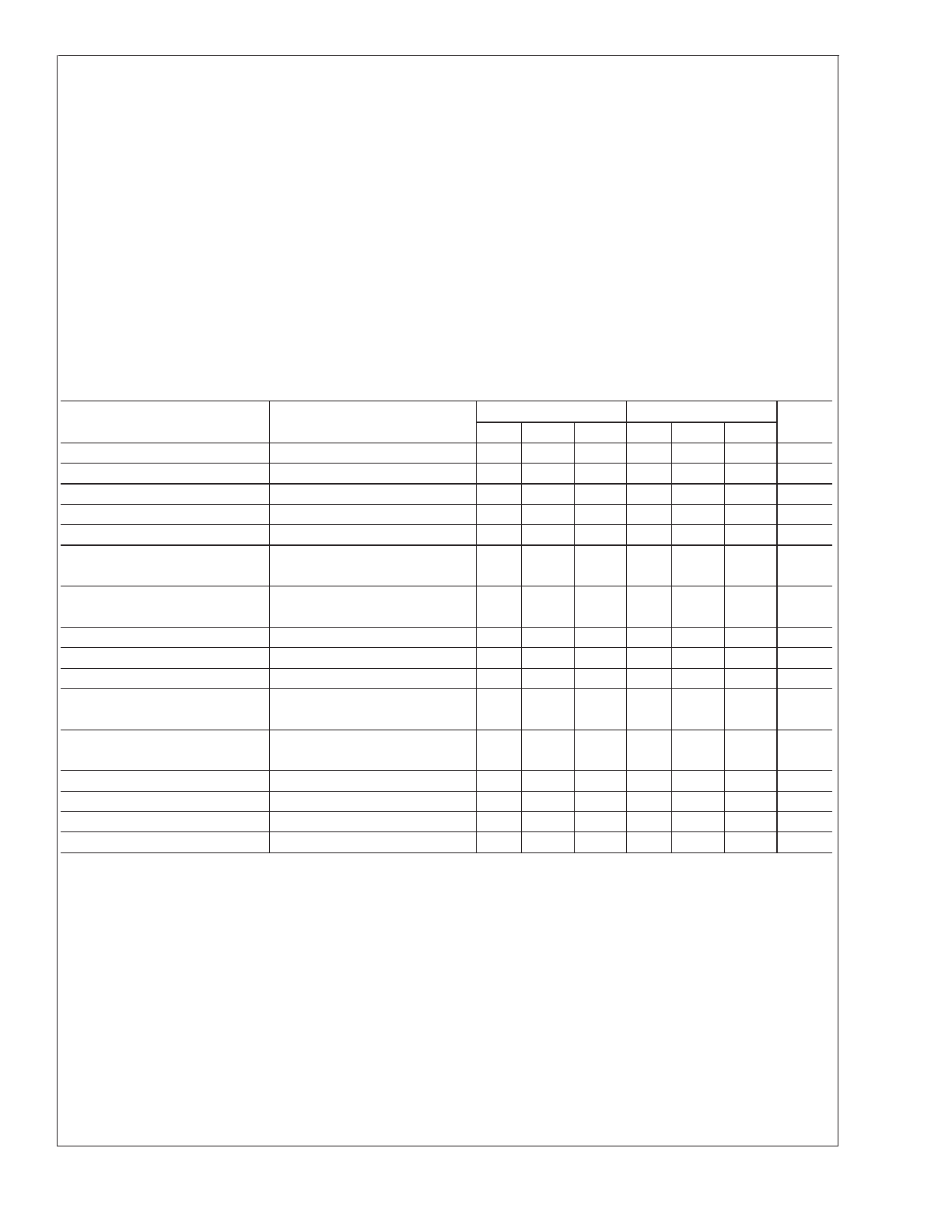
Absolute Maximum Ratings
LM319A/319
(Note 9)
If Military/Aerospace specified devices are required,
please contact the National Semiconductor Sales Office/
Distributors for availability and specifications.
Total Supply Voltage
36V
Output to Negative Supply Voltage
36V
Ground to Negative Supply Voltage
25V
Ground to Positive Supply Voltage
18V
Differential Input Voltage
±
5V
Input Voltage (Note 10)
±
15V
Power Dissipation (Note 11)
500 mW
Output Short Circuit Duration
10 sec
ESD rating (1.5 k
Ω
in series with
100 pF)
800V
Storage Temperature Range
−65˚C to 150˚C
Lead Temperature
(Soldering, 10 sec.)
260˚C
Soldering Information
Dual-In-Line Package
Soldering (10 sec.)
260˚C
Small Outline Package
Vapor Phase (60 sec.)
215˚C
Infrared (15 sec.)
220˚C
See AN-450 “Surface Mounting Methods and Their Effect
on Product Reliability” for other methods of soldering
surface mount devices.
Operating Temperature Range
LM319A, LM319
0˚C to 70˚C
Electrical Characteristics
(Note 12)
Parameter
Conditions
LM319A
LM319
Units
Min
Typ
Max
Min
Typ
Max
Input Offset Voltage (Note 13)
T
A
= 25˚C, R
S
≤
5k
0.5
1.0
2.0
8.0
mV
Input Offset Current (Note 13)
T
A
= 25˚C
20
40
80
200
nA
Input Bias Current
T
A
= 25˚C
150
500
250
1000
nA
Voltage Gain
T
A
= 25˚C (Note 15)
20
40
8
40
V/mV
Response Time (Note 14)
T
A
= 25˚C, V
S
=
±
15V
80
80
ns
Saturation Voltage
V
IN
≤
−10 mV, I
OUT
= 25 mA
T
A
= 25˚C
0.75
1.5
0.75
1.5
V
Output Leakage Current
V
IN
≥
10 mV, V
OUT
= 35V,
V
− = V
GND = 0V, T
A
= 25˚C
0.2
10
0.2
10
µA
Input Offset Voltage (Note 13)
R
S
≤
5k
10
10
mV
Input Offset Current (Note 13)
300
300
nA
Input Bias Current
1000
1200
nA
Input Voltage Range
V
S
=
±
15V
±
13
±
13
V
V
+
= 5V, V
−
= 0
1
3
1
3
V
Saturation Voltage
V
+
≥
4.5V, V
−
= 0
0.3
0.4
0.3
0.4
V
V
IN
≤
−10 mV, I
SINK
≤
3.2 mA
Differential Input Voltage
±
5
±
5
V
Positive Supply Current
T
A
= 25˚C, V
+
= 5V, V
−
= 0
4.3
4.3
mA
Positive Supply Current
T
A
= 25˚C, V
S
=
±
15V
8
12.5
8
12.5
mA
Negative Supply Current
T
A
= 25˚C, V
S
=
±
15V
3
5
3
5
mA
Note 10: For supply voltages less than
±
15 the absolute maximum input voltage is equal to the supply voltage.
Note 11: The maximum junction temperature of the LM319A and LM319 is 85˚C. For operating at elevated temperatures, devices in the H10 package must be de-
rated based on a thermal resistance of 160˚C/W, junction to ambient, or 19˚C/W, junction to case. The thermal resistance of the N14 and J14 package is 100˚C/W,
junction to ambient. The thermal resistance of the M14 package is 115˚C/W, junction to ambient.
Note 12: These specifications apply for V
S
=
±
15V, and 0˚C
≤
T
A
≤
70˚C, unless otherwise stated. The offset voltage, offset current and bias current specifications
apply for any supply voltage from a single 5V supply up to
±
15V supplies. Do not operate the device with more than 16V from ground to V
S
.
Note 13: The offset voltages and offset currents given are the maximum values required to drive the output within a volt of either supply with a 1 mA load. Thus, these
parameters define an error band and take into account the worst case effects of voltage gain and input impedance.
Note 14: The response time specified is for a 100 mV input step with 5 mV overdrive.
Note 15: Output is pulled up to 15V through a 1.4 k
Ω
resistor.
LM1
19/LM219/LM319
www.national.com
3
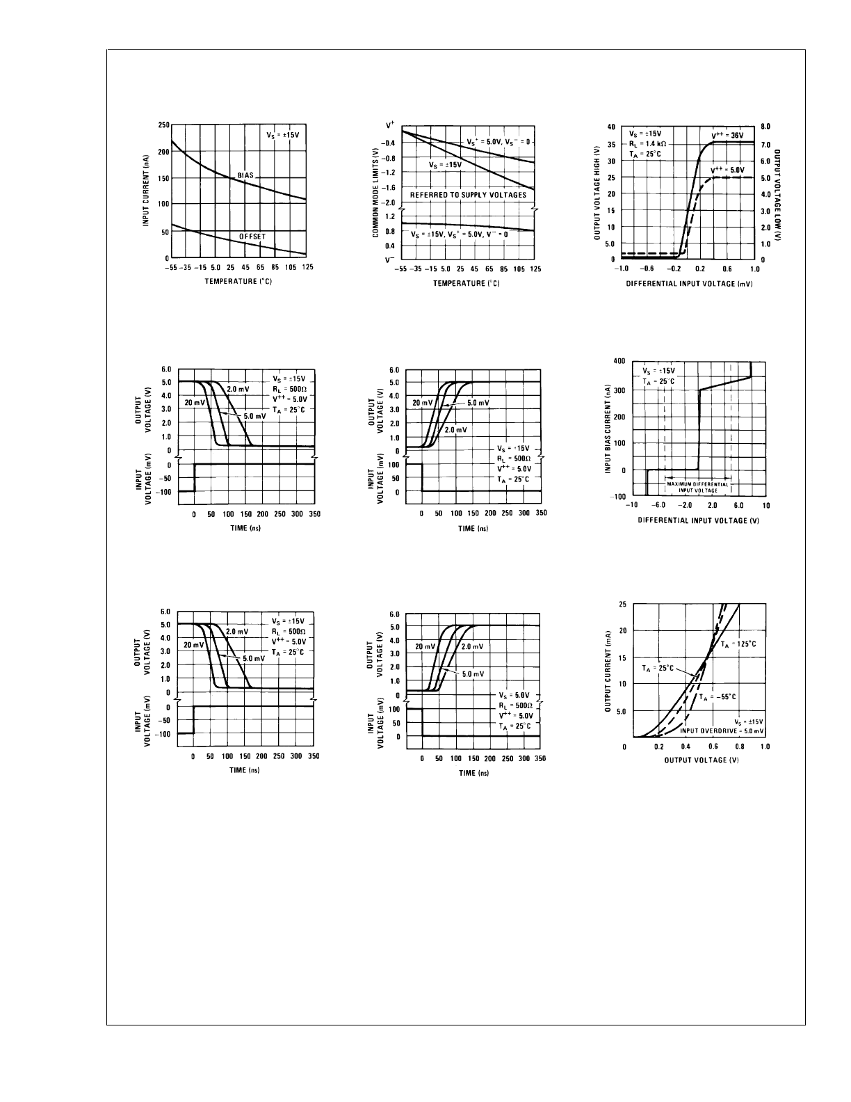
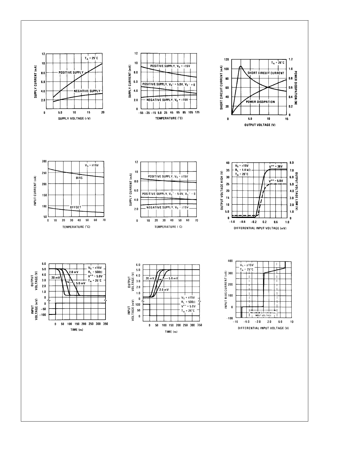
Typical Performance Characteristics
LM119A/LM119/LM219
Input Currents
DS005705-10
Common Mode Limits
DS005705-11
Transfer Function
DS005705-12
Response Time for Various
Input Overdrives
DS005705-13
Response Time for Various
Input Overdrives
DS005705-14
Input Characteristics
DS005705-15
Response Time for Various
Input Overdrives
DS005705-16
Response Time for Various
Input Overdrives
DS005705-17
Output Saturation Voltage
DS005705-18
LM1
19/LM219/LM319
www.national.com
4
Typical Performance Characteristics
LM119A/LM119/LM219 (Continued)
Typical Performance Characteristics
LM319A, LM319
Supply Current
DS005705-19
Supply Current
DS005705-20
Output Limiting
Characteristics
DS005705-21
Input Currents
DS005705-22
Supply Currents
DS005705-23
Transfer Function
DS005705-24
Response Time for Various
Input Overdrives
DS005705-25
Response Time for Various
Input Overdrives
DS005705-26
Input Characteristics
DS005705-27
LM1
19/LM219/LM319
www.national.com
5
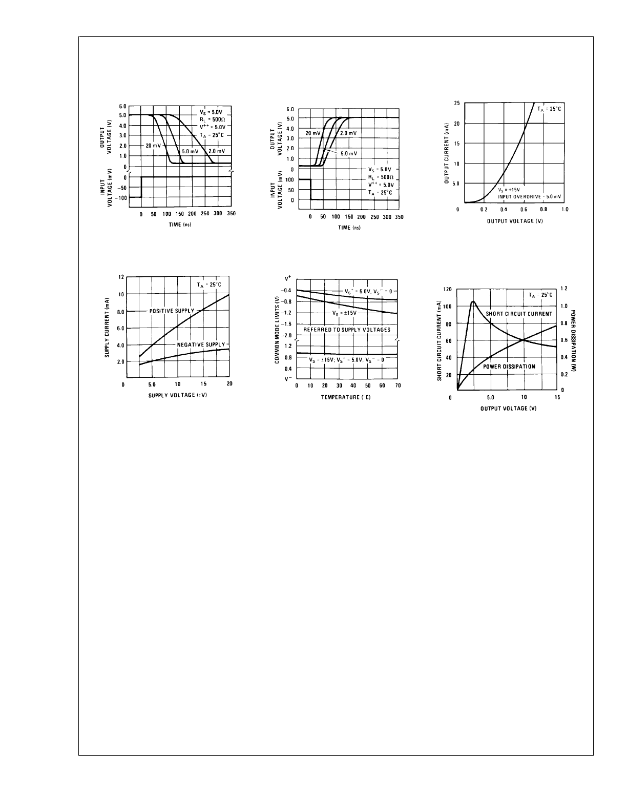
Typical Performance Characteristics
LM319A, LM319 (Continued)
Response Time for Various
Input Overdrives
DS005705-28
Response Time for Various
Input Overdrives
DS005705-29
Output Saturation Voltage
DS005705-30
Supply Current
DS005705-31
Common Mode Limits
DS005705-32
Output Limiting
Characteristics
DS005705-33
LM1
19/LM219/LM319
www.national.com
6
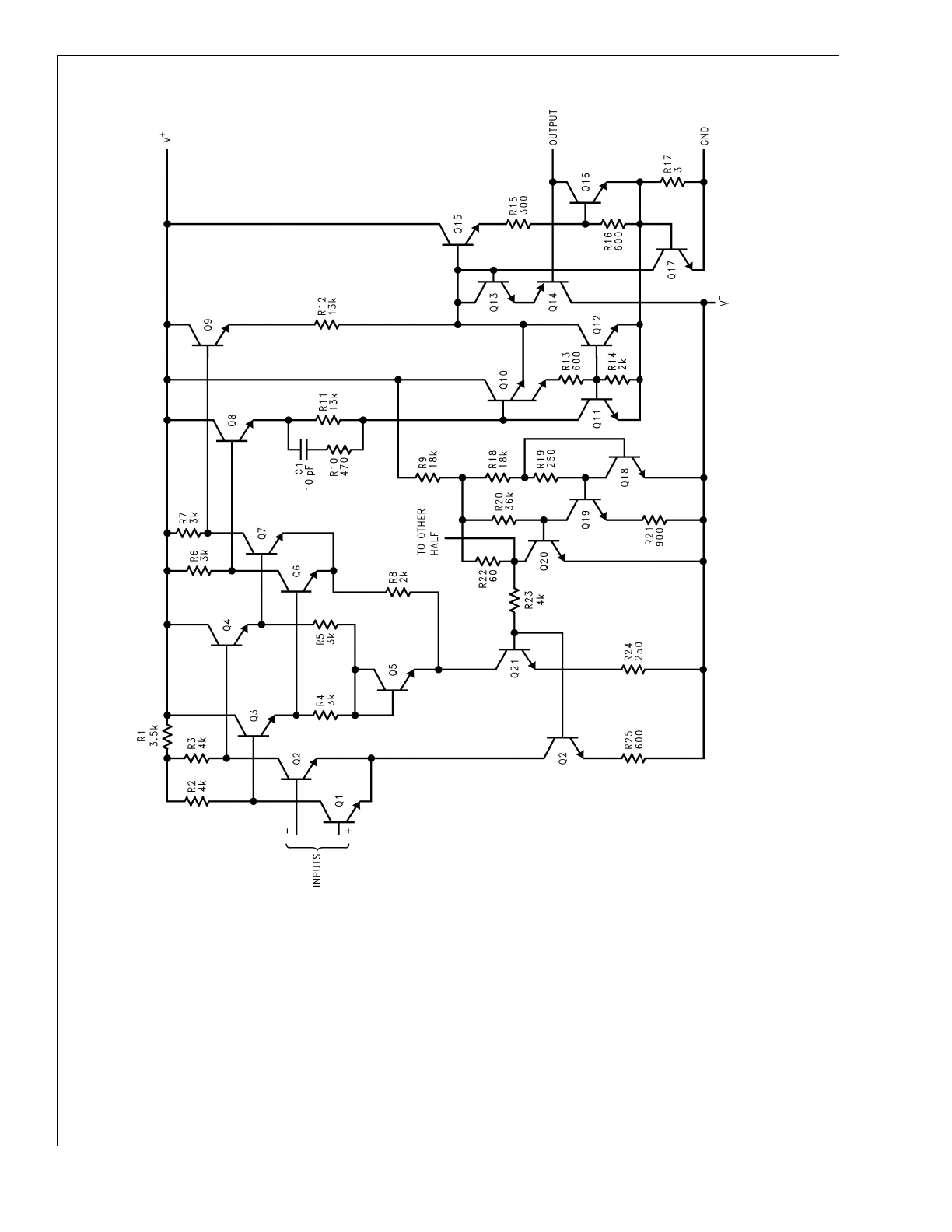
Schematic Diagram
DS005705-1
*Do
not
operate
the
LM1
19
with
more
than
16V
between
GND
and
V
+
LM1
19/LM219/LM319
www.national.com
7
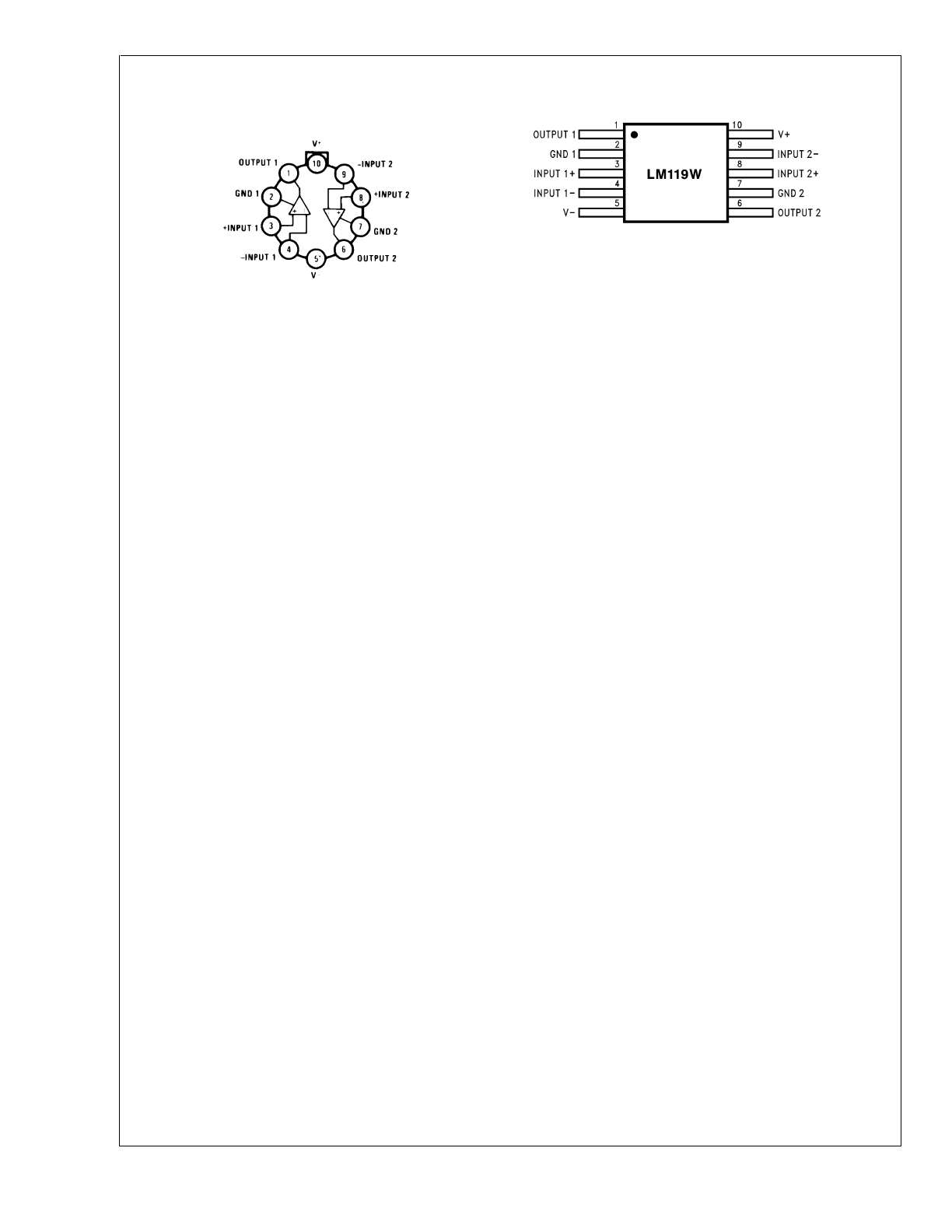
Connection Diagrams
Metal Can Package
DS005705-7
Case is connected to pin 5 (V
−
)
Top View
Order Number LM119H, LM119H/883 (Note 1),
or LM319H
See NS Package Number H10C
DS005705-9
Order Number LM119W/883
See NS Package Number W10A
LM1
19/LM219/LM319
www.national.com
8
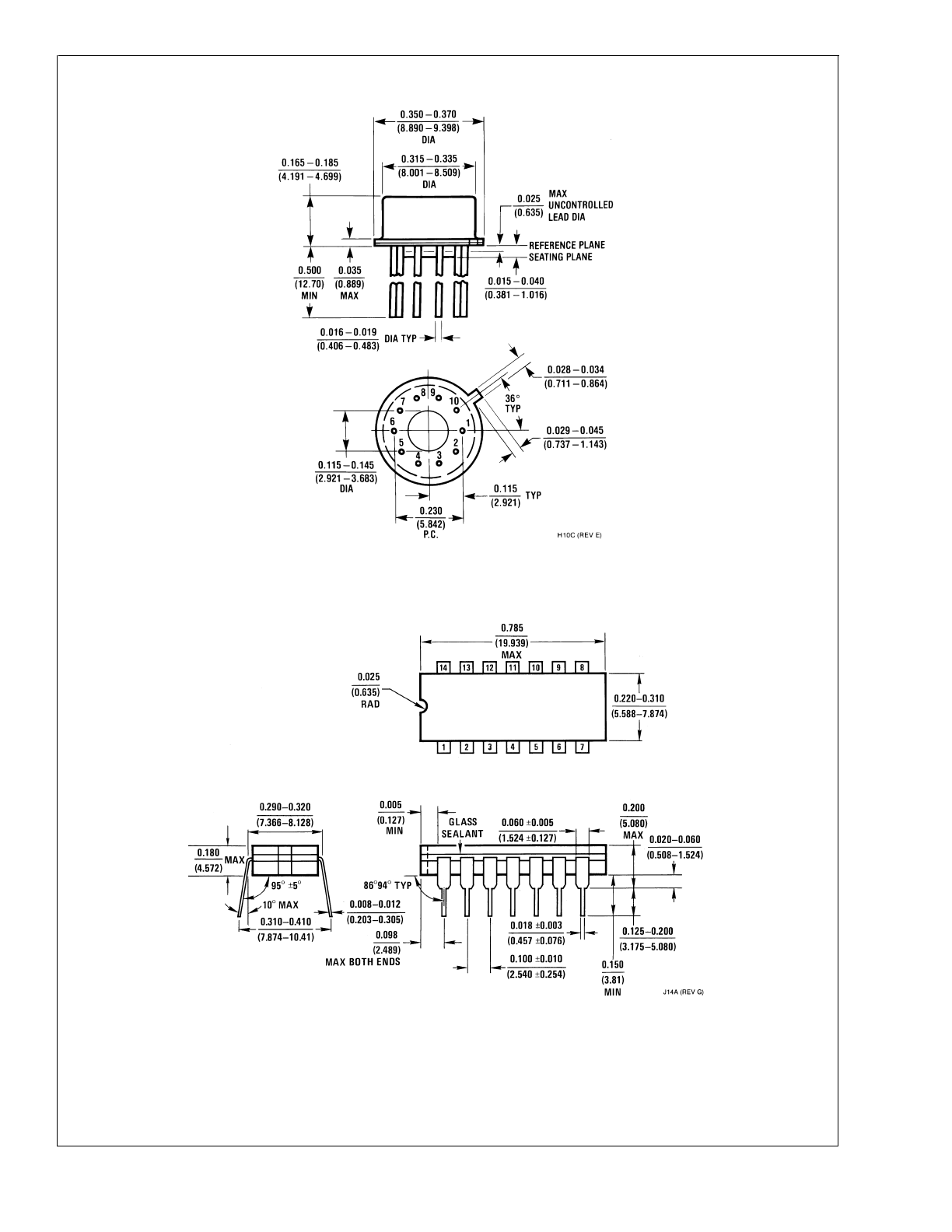
Physical Dimensions
inches (millimeters) unless otherwise noted
Metal Can Package (H)
Order Number LM119H, LM119H/883, LM319AH or LM319H
NS Package Number H10C
Cavity Dual-In-Line Package (J)
Order Number LM119J, LM119J/883, LM219J, LM319AJ or LM319J
NS Package Number J14A
LM1
19/LM219/LM319
www.national.com
9
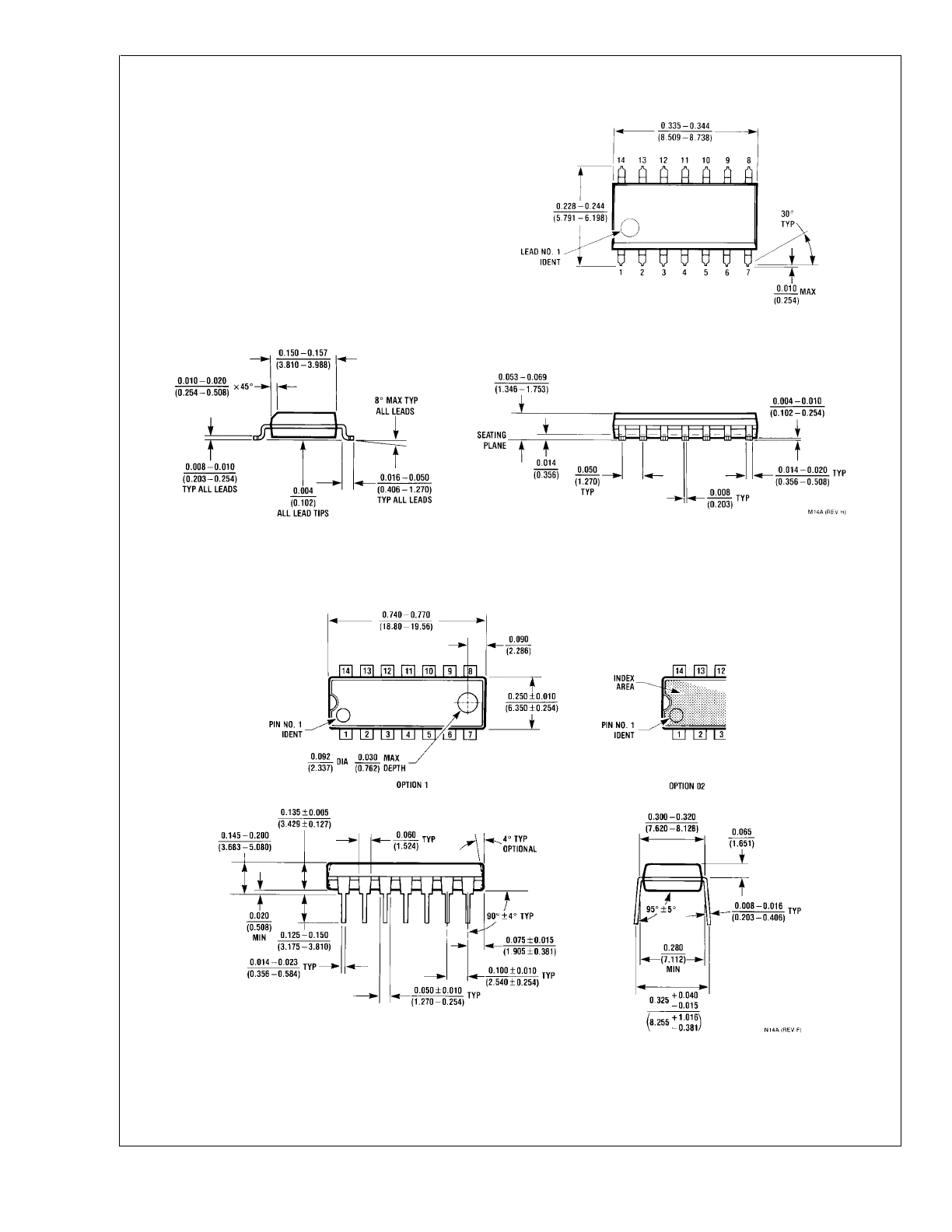
Physical Dimensions
inches (millimeters) unless otherwise noted (Continued)
Dual-In-Line Package (M)
Order Number LM319AM or LM319M
NS Package Number M14A
Molded Dual-In-Line Package (N)
Order Number LM319AN or LM319N
NS Package Number N14A
LM1
19/LM219/LM319
www.national.com
10
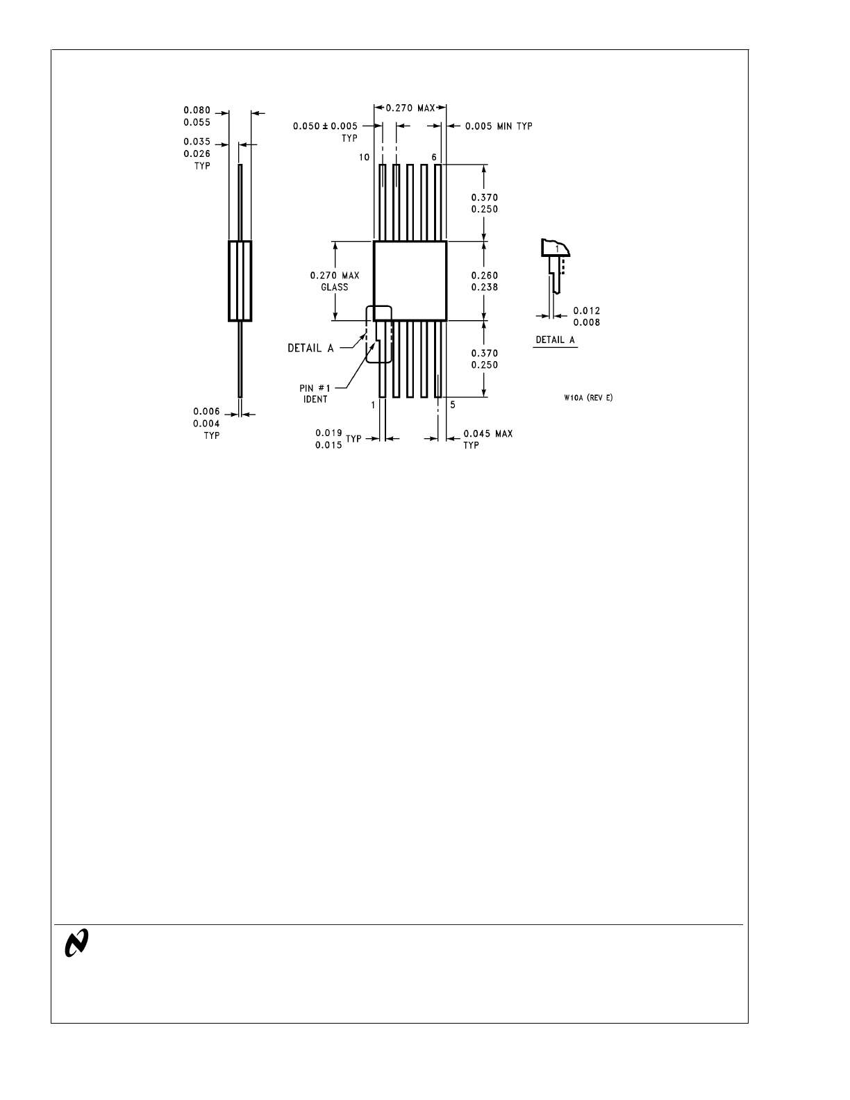
Physical Dimensions
inches (millimeters) unless otherwise noted (Continued)
LIFE SUPPORT POLICY
NATIONAL’S PRODUCTS ARE NOT AUTHORIZED FOR USE AS CRITICAL COMPONENTS IN LIFE SUPPORT
DEVICES OR SYSTEMS WITHOUT THE EXPRESS WRITTEN APPROVAL OF THE PRESIDENT AND GENERAL
COUNSEL OF NATIONAL SEMICONDUCTOR CORPORATION. As used herein:
1. Life support devices or systems are devices or
systems which, (a) are intended for surgical implant
into the body, or (b) support or sustain life, and
whose failure to perform when properly used in
accordance with instructions for use provided in the
labeling, can be reasonably expected to result in a
significant injury to the user.
2. A critical component is any component of a life
support device or system whose failure to perform
can be reasonably expected to cause the failure of
the life support device or system, or to affect its
safety or effectiveness.
National Semiconductor
Corporation
Americas
Tel: 1-800-272-9959
Fax: 1-800-737-7018
Email: support@nsc.com
National Semiconductor
Europe
Fax: +49 (0) 180-530 85 86
Email: europe.support@nsc.com
Deutsch Tel: +49 (0) 69 9508 6208
English
Tel: +44 (0) 870 24 0 2171
Français Tel: +33 (0) 1 41 91 8790
National Semiconductor
Asia Pacific Customer
Response Group
Tel: 65-2544466
Fax: 65-2504466
Email: ap.support@nsc.com
National Semiconductor
Japan Ltd.
Tel: 81-3-5639-7560
Fax: 81-3-5639-7507
www.national.com
Order Number LM119W/883, LM119WG/883
NS Package Number W10A, WG10A
LM1
19/LM219/LM319
High
Speed
Dual
Comparator
National does not assume any responsibility for use of any circuitry described, no circuit patent licenses are implied and National reserves the right at any time without notice to change said circuitry and specifications.