
LM1117/LM1117I
800mA Low-Dropout Linear Regulator
General Description
The LM1117 is a series of low dropout voltage regulators
with a dropout of 1.2V at 800mA of load current. It has the
same pin-out as National Semiconductor’s industry standard
LM317.
The LM1117 is available in an adjustable version, which can
set the output voltage from 1.25V to 13.8V with only two
external resistors. In addition, it is also available in five fixed
voltages, 1.8V, 2.5V, 2.85V, 3.3V, and 5V.
The LM1117 offers current limiting and thermal shutdown. Its
circuit includes a zener trimmed bandgap reference to as-
sure output voltage accuracy to within
±
1%.
The LM1117 series is available in SOT-223, TO-220, and
TO-252 D-PAK packages. A minimum of 10µF tantalum ca-
pacitor is required at the output to improve the transient
response and stability.
Features
n
Available in 1.8V, 2.5V, 2.85V, 3.3V, 5V, and Adjustable
Versions
n
Space Saving SOT-223 Package
n
Current Limiting and Thermal Protection
n
Output Current
800mA
n
Line Regulation
0.2% (Max)
n
Load Regulation
0.4% (Max)
n
Temperature Range
— LM1117
0˚C to 125˚C
— LM1117I
−40˚C to 125˚C
Applications
n
2.85V Model for SCSI-2 Active Termination
n
Post Regulator for Switching DC/DC Converter
n
High Efficiency Linear Regulators
n
Battery Charger
n
Battery Powered Instrumentation
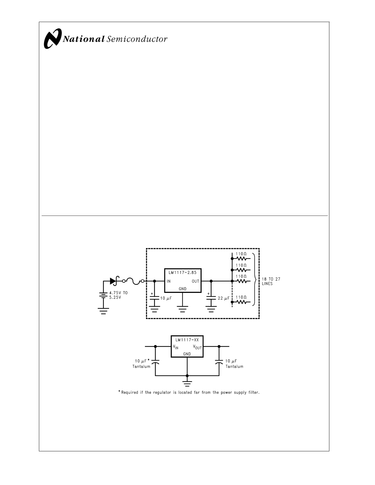
Typical Application
Active Terminator for SCSI-2 Bus
DS100919-5
Fixed Output Regulator
DS100919-28
July 2001
LM1
1
17/LM1
1
17I
800mA
Low-Dropout
Linear
Regulator
© 2001 National Semiconductor Corporation
DS100919
www.national.com
Ordering Information
Package
Temperature
Range
Part Number
Packaging Marking
Transport Media
NSC
Drawing
3-lead
SOT-223
0˚C to +125˚C
LM1117MPX-ADJ
N03A
Tape and Reel
MA04A
LM1117MPX-1.8
N12A
Tape and Reel
LM1117MPX-2.5
N13A
Tape and Reel
LM1117MPX-2.85
N04A
Tape and Reel
LM1117MPX-3.3
N05A
Tape and Reel
LM1117MPX-5.0
N06A
Tape and Reel
−40˚C to +125˚C
LM1117IMPX-ADJ
N03B
Tape and Reel
LM1117IMPX-5.0
N06B
Tape and Reel
3-lead TO-220
0˚C to +125˚C
LM1117T-ADJ
LM1117T-ADJ
Rails
T03B
LM1117T-2.85
LM1117T-2.85
Rails
LM1117T-3.3
LM1117T-3.3
Rails
LM1117T-5.0
LM1117T-5.0
Rails
3-lead TO-252
0˚C to +125˚C
LM1117DTX-ADJ
LM1117DT-ADJ
Tape and Reel
TD03B
LM1117DTX-1.8
LM1117DT-1.8
Tape and Reel
LM1117DTX-2.5
LM1117DT-2.5
Tape and Reel
LM1117DTX-2.85
LM1117DT-2.85
Tape and Reel
LM1117DTX-3.3
LM1117DT-3.3
Tape and Reel
LM1117DTX-5.0
LM1117DT-5.0
Tape and Reel
−40˚C to +125˚C
LM1117IDTX-ADJ
LM1117IDT-ADJ
Tape and Reel
LM1117IDTX-5.0
LM1117IDT-5.0
Tape and Reel
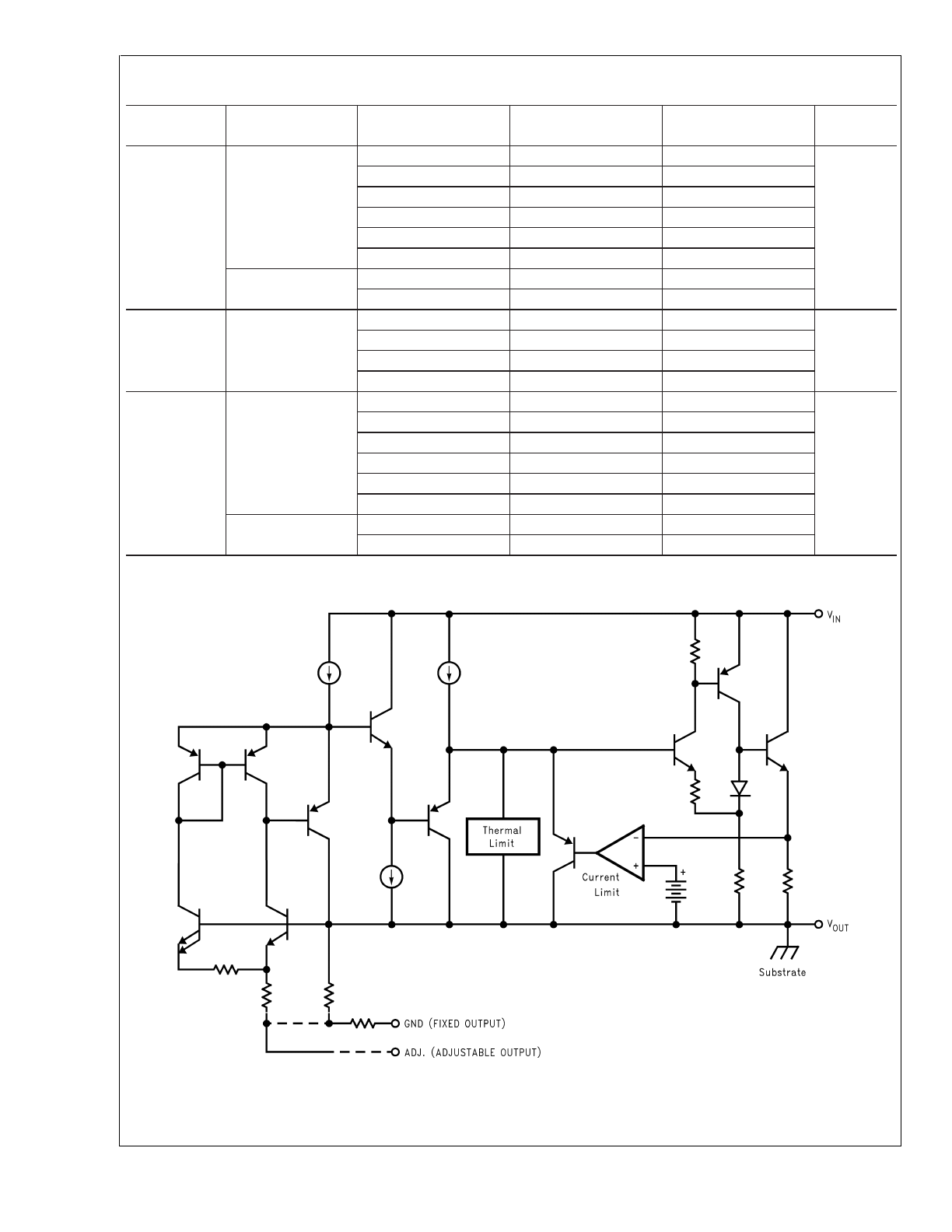
Block Diagram
DS100919-1
LM1
1
17/LM1
1
17I
www.national.com
2
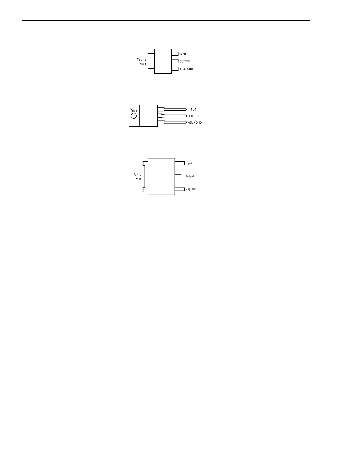
Connection Diagrams
SOT-223
DS100919-4
Top View
TO-220
DS100919-2
Top View
TO-252
DS100919-38
Top View
LM1
1
17/LM1
1
17I
www.national.com
3
Absolute Maximum Ratings
(Note 1)
If Military/Aerospace specified devices are required,
please contact the National Semiconductor Sales Office/
Distributors for availability and specifications.
Maximum Input Voltage (V
IN
to GND)
LM1117-ADJ, LM1117-1.8,
LM1117-2.5, LM1117-3.3,
LM1117-5.0, LM1117I-ADJ,
LM1117I-5.0
20V
Power Dissipation (Note 2)
Internally Limited
Junction Temperature (T
J
)
(Note 2)
150˚C
Storage Temperature Range
-65˚C to 150˚C
Lead Temperature
TO-220 (T) Package
260˚C, 10 sec
SOT-223 (IMP) Package
260˚C, 4 sec
ESD Tolerance (Note 3)
2000V
Operating Ratings
(Note 1)
Input Voltage (V
IN
to GND)
LM1117-ADJ, LM1117-1.8,
LM1117-2.5, LM1117-3.3,
LM1117-5.0, LM1117I-ADJ,
LM1117I-5.0
15V
LM1117-2.85
10V
Junction Temperature Range (T
J
)(Note 2)
LM1117
0˚C to 125˚C
LM1117I
−40˚C to 125˚C
LM1117 Electrical Characteristics
Typicals and limits appearing in normal type apply for T
J
= 25˚C. Limits appearing in Boldface type apply over the entire junc-
tion temperature range for operation, 0˚C to 125˚C.
Symbol
Parameter
Conditions
Min
(Note 5)
Typ
(Note 4)
Max
(Note 5)
Units
V
REF
Reference Voltage
LM1117-ADJ
I
OUT
= 10mA, V
IN
-V
OUT
= 2V, T
J
= 25˚C
10mA
≤
I
OUT
≤
800mA, 1.4V
≤
V
IN
-V
OUT
≤
10V
1.238
1.225
1.250
1.250
1.262
1.270
V
V
V
OUT
Output Voltage
LM1117-1.8
I
OUT
= 10mA, V
IN
= 3.8V, T
J
= 25˚C
0
≤
I
OUT
≤
800mA, 3.2V
≤
V
IN
≤
10V
1.782
1.746
1.800
1.800
1.818
1.854
V
V
LM1117-2.5
I
OUT
= 10mA, V
IN
= 4.5V, T
J
= 25˚C
0
≤
I
OUT
≤
800mA, 3.9V
≤
V
IN
≤
10V
2.475
2.450
2.500
2.500
2.525
2.550
V
V
LM1117-2.85
I
OUT
= 10mA, V
IN
= 4.85V, T
J
= 25˚C
0
≤
I
OUT
≤
800mA, 4.25V
≤
V
IN
≤
10V
0
≤
I
OUT
≤
500mA, V
IN
= 4.10V
2.820
2.790
2.790
2.850
2.850
2.850
2.880
2.910
2.910
V
V
V
LM1117-3.3
I
OUT
= 10mA, V
IN
= 5V T
J
= 25˚C
0
≤
I
OUT
≤
800mA, 4.75V
≤
V
IN
≤
10V
3.267
3.235
3.300
3.300
3.333
3.365
V
V
LM1117-5.0
I
OUT
= 10mA, V
IN
= 7V, T
J
= 25˚C
0
≤
I
OUT
≤
800mA, 6.5V
≤
V
IN
≤
12V
4.950
4.900
5.000
5.000
5.050
5.100
V
V
∆
V
OUT
Line Regulation
(Note 6)
LM1117-ADJ
I
OUT
= 10mA, 1.5V
≤
V
IN
-V
OUT
≤
13.75V
0.035
0.2
%
LM1117-1.8
I
OUT
= 0mA, 3.2V
≤
V
IN
≤
10V
1
6
mV
LM1117-2.5
I
OUT
= 0mA, 3.9V
≤
V
IN
≤
10V
1
6
mV
LM1117-2.85
I
OUT
= 0mA, 4.25V
≤
V
IN
≤
10V
1
6
mV
LM1117-3.3
I
OUT
= 0mA, 4.75V
≤
V
IN
≤
15V
1
6
mV
LM1117-5.0
I
OUT
= 0mA, 6.5V
≤
V
IN
≤
15V
1
10
mV
LM1
1
17/LM1
1
17I
www.national.com
4
LM1117 Electrical Characteristics
(Continued)
Typicals and limits appearing in normal type apply for T
J
= 25˚C. Limits appearing in Boldface type apply over the entire junc-
tion temperature range for operation, 0˚C to 125˚C.
Symbol
Parameter
Conditions
Min
(Note 5)
Typ
(Note 4)
Max
(Note 5)
Units
∆
V
OUT
Load Regulation
(Note 6)
LM1117-ADJ
V
IN
-V
OUT
= 3V, 10
≤
I
OUT
≤
800mA
0.2
0.4
%
LM1117-1.8
V
IN
= 3.2V, 0
≤
I
OUT
≤
800mA
1
10
mV
LM1117-2.5
V
IN
= 3.9V, 0
≤
I
OUT
≤
800mA
1
10
mV
LM1117-2.85
V
IN
= 4.25V, 0
≤
I
OUT
≤
800mA
1
10
mV
LM1117-3.3
V
IN
= 4.75V, 0
≤
I
OUT
≤
800mA
1
10
mV
LM1117-5.0
V
IN
= 6.5V, 0
≤
I
OUT
≤
800mA
1
15
mV
V
IN
-V
OUT
Dropout Voltage
(Note 7)
I
OUT
= 100mA
1.10
1.20
V
I
OUT
= 500mA
1.15
1.25
V
I
OUT
= 800mA
1.20
1.30
V
I
LIMIT
Current Limit
V
IN
-V
OUT
= 5V, T
J
= 25˚C
800
1200
1500
mA
Minimum Load
Current (Note 8)
LM1117-ADJ
V
IN
= 15V
1.7
5
mA
Quiescent Current
LM1117-1.8
V
IN
≤
15V
5
10
mA
LM1117-2.5
V
IN
≤
15V
5
10
mA
LM1117-2.85
V
IN
≤
10V
5
10
mA
LM1117-3.3
V
IN
≤
15V
5
10
mA
LM1117-5.0
V
IN
≤
15V
5
10
mA
Thermal Regulation
T
A
= 25˚C, 30ms Pulse
0.01
0.1
%/W
Ripple Regulation
f
RIPPLE
=1 20Hz, V
IN
-V
OUT
= 3V
V
RIPPLE
= 1V
PP
60
75
dB
Adjust Pin Current
60
120
µA
Adjust Pin Current
Change
10
≤
I
OUT
≤
800mA,
1.4V
≤
V
IN
-V
OUT
≤
10V
0.2
5
µA
Temperature Stability
0.5
%
Long Term Stability
T
A
= 125˚C, 1000Hrs
0.3
%
RMS Output Noise
(% of V
OUT
), 10Hz
≤
f
≤
10kHz
0.003
%
Thermal Resistance
Junction-to-Case
3-Lead SOT-223
3-Lead TO-220
3-Lead TO-252
15.0
3.0
10
˚C/W
˚C/W
˚C/W
Thermal Resistance
Junction-to-Ambient
(No heat sink;
No air flow)
3-Lead SOT-223
3-Lead TO-220
3-Lead TO-252 (Note 9)
136
79
92
˚C/W
˚C/W
˚C/W
LM1
1
17/LM1
1
17I
www.national.com
5
LM1117I Electrical Characteristics
Typicals and limits appearing in normal type apply for T
J
= 25˚C. Limits appearing in Boldface type apply over the entire junc-
tion temperature range for operation, −40˚C to 125˚C.
Symbol
Parameter
Conditions
Min
(Note 5)
Typ
(Note 4)
Max
(Note 5)
Units
V
REF
Reference Voltage
LM1117I-ADJ
I
OUT
= 10mA, V
IN
-V
OUT
= 2V, T
J
= 25˚C
10mA
≤
I
OUT
≤
800mA, 1.4V
≤
V
IN
-V
OUT
≤
10V
1.238
1.200
1.250
1.250
1.262
1.290
V
V
V
OUT
Output Voltage
LM1117I-5.0
I
OUT
= 10mA, V
IN
= 7V, T
J
= 25˚C
0
≤
I
OUT
≤
800mA, 6.5V
≤
V
IN
≤
12V
4.950
4.800
5.000
5.000
5.050
5.200
V
V
∆
V
OUT
Line Regulation
(Note 6)
LM1117I-ADJ
I
OUT
= 10mA, 1.5V
≤
V
IN
-V
OUT
≤
13.75V
0.035
0.3
%
LM1117I-5.0
I
OUT
= 0mA, 6.5V
≤
V
IN
≤
15V
1
15
mV
∆
V
OUT
Load Regulation
(Note 6)
LM1117I-ADJ
V
IN
-V
OUT
= 3V, 10
≤
I
OUT
≤
800mA
0.2
0.5
%
LM1117I-5.0
V
IN
= 6.5V, 0
≤
I
OUT
≤
800mA
1
20
mV
V
IN
-V
OUT
Dropout Voltage
(Note 7)
I
OUT
= 100mA
1.10
1.30
V
I
OUT
= 500mA
1.15
1.35
V
I
OUT
= 800mA
1.20
1.40
V
I
LIMIT
Current Limit
V
IN
-V
OUT
= 5V, T
J
= 25˚C
800
1200
1500
mA
Minimum Load
Current (Note 8)
LM1117I-ADJ
V
IN
= 15V
1.7
5
mA
Quiescent Current
LM1117I-5.0
V
IN
≤
15V
5
15
mA
Thermal Regulation
T
A
= 25˚C, 30ms Pulse
0.01
0.1
%/W
Ripple Regulation
f
RIPPLE
=1 20Hz, V
IN
-V
OUT
= 3V
V
RIPPLE
= 1V
PP
60
75
dB
Adjust Pin Current
60
120
µA
Adjust Pin Current
Change
10
≤
I
OUT
≤
800mA,
1.4V
≤
V
IN
-V
OUT
≤
10V
0.2
10
µA
Temperature Stability
0.5
%
Long Term Stability
T
A
= 125˚C, 1000Hrs
0.3
%
RMS Output Noise
(% of V
OUT
), 10Hz
≤
f
≤
10kHz
0.003
%
Thermal Resistance
Junction-to-Case
3-Lead SOT-223
-Lead TO-252
15.0
10
˚C/W
˚C/W
Thermal Resistance
Junction-to-Ambient
(No heat sink;
No air flow)
3-Lead SOT-223
3-Lead TO-252 (Note 9)
136
92
˚C/W
˚C/W
Note 1: Absolute Maximum Ratings indicate limits beyond which damage to the device may occur. Operating Ratings indicate conditions for which the device is
intended to be functional, but specific performance is not guaranteed. For guaranteed specifications and the test conditions, see the Electrical Characteristics.
Note 2: The maximum power dissipation is a function of T
J(max)
,
θ
JA
, and T
A
. The maximum allowable power dissipation at any ambient temperature is
P
D
= (T
J(max)
–T
A
)/
θ
JA
. All numbers apply for packages soldered directly into a PC board.
Note 3: For testing purposes, ESD was applied using human body model, 1.5k
Ω
in series with 100pF.
Note 4: Typical Values represent the most likely parametric norm.
Note 5: All limits are guaranteed by testing or statistical analysis.
Note 6: Load and line regulation are measured at constant junction room temperature.
Note 7: The dropout voltage is the input/output differential at which the circuit ceases to regulate against further reduction in input voltage. It is measured when the
output voltage has dropped 100mV from the nominal value obtained at V
IN
= V
OUT
+1.5V.
Note 8: The minimum output current required to maintain regulation.
Note 9: Minimum pad size of 0.038in
2
LM1
1
17/LM1
1
17I
www.national.com
6
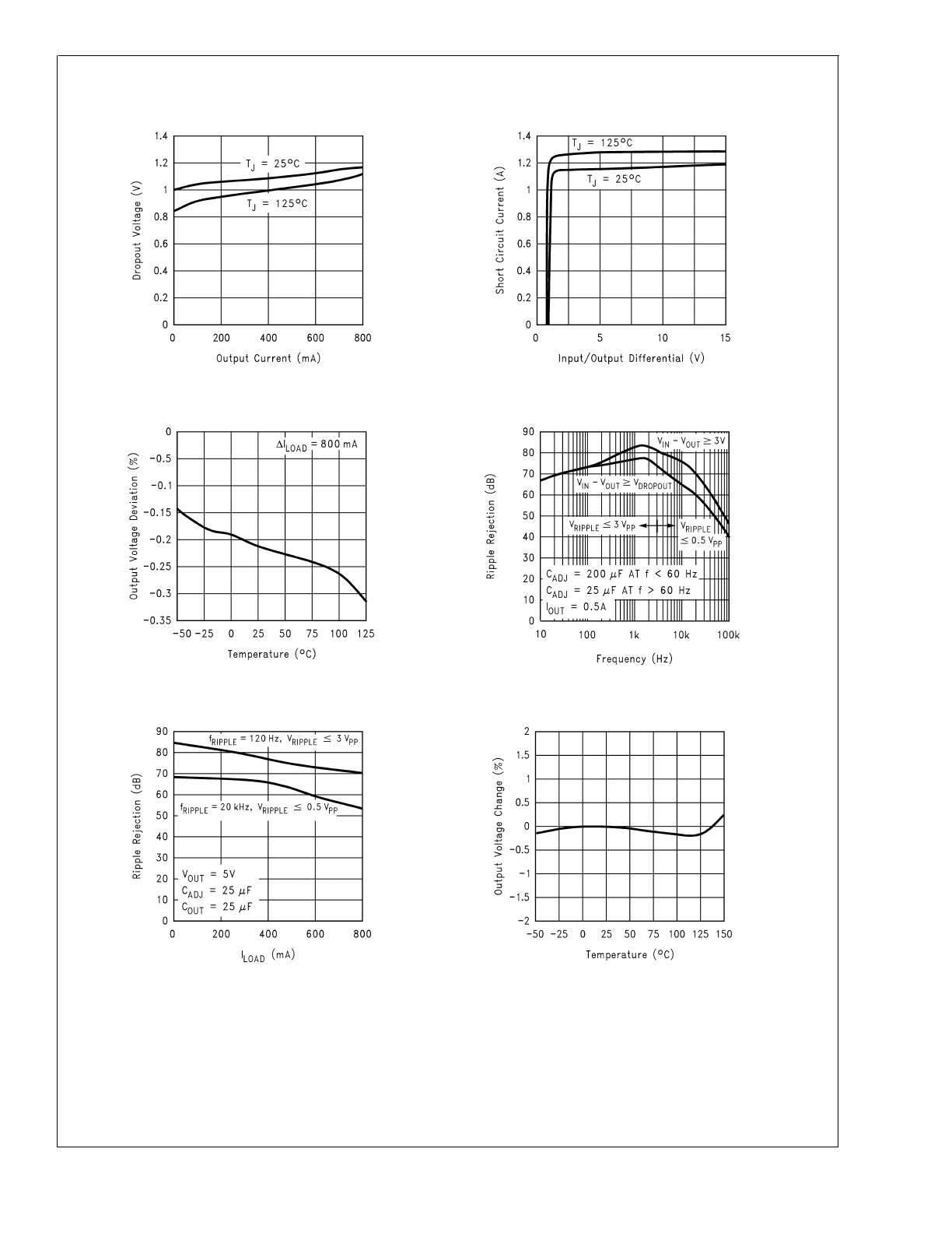
Typical Performance Characteristics
Dropout Voltage (V
IN
-V
OUT
)
DS100919-22
Short-Circuit Current
DS100919-23
Load Regulation
DS100919-43
LM1117-ADJ Ripple Rejection
DS100919-6
LM1117-ADJ Ripple Rejection vs. Current
DS100919-7
Temperature Stability
DS100919-25
LM1
1
17/LM1
1
17I
www.national.com
7
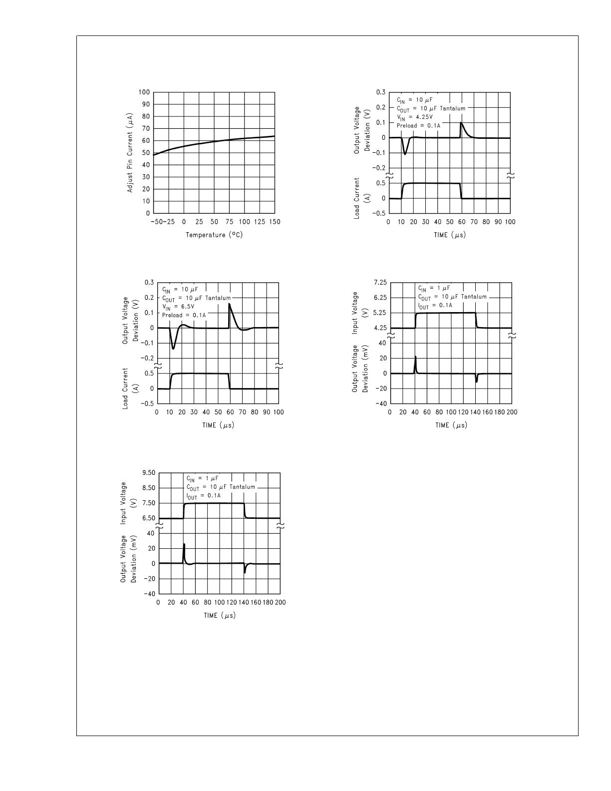
Typical Performance Characteristics
(Continued)
Adjust Pin Current
DS100919-26
LM1117-2.85 Load Transient Response
DS100919-8
LM1117-5.0 Load Transient Response
DS100919-9
LM1117-2.85 Line Transient Response
DS100919-10
LM1117-5.0 Line Transient Response
DS100919-11
LM1
1
17/LM1
1
17I
www.national.com
8
APPLICATION NOTE
1.0 External Capacitors/Stability
1.1 Input Bypass Capacitor
An input capacitor is recommended. A 10µF tantalum on the
input is a suitable input bypassing for almost all applications.
1.2 Adjust Terminal Bypass Capacitor
The adjust terminal can be bypassed to ground with a by-
pass capacitor (C
ADJ
) to improve ripple rejection. This by-
pass capacitor prevents ripple from being amplified as the
output voltage is increased. At any ripple frequency, the
impedance of the C
ADJ
should be less than R1 to prevent the
ripple from being amplified:
1/(2
π
*f
RIPPLE
*C
ADJ
)
<
R1
The R1 is the resistor between the output and the adjust pin.
Its value is normally in the range of 100-200
Ω
. For example,
with R1 = 124
Ω
and f
RIPPLE
= 120Hz, the C
ADJ
should be
>
11µF.
1.3 Output Capacitor
The output capacitor is critical in maintaining regulator sta-
bility, and must meet the required conditions for both mini-
mum amount of capacitance and ESR (Equivalent Series
Resistance). The minimum output capacitance required by
the LM1117 is 10µF, if a tantalum capacitor is used. Any
increase of the output capacitance will merely improve the
loop stability and transient response. The ESR of the output
capacitor should be greater than 0.5
Ω
and less than 5
Ω
. In
the case of the adjustable regulator, when the C
ADJ
is used,
a larger output capacitance (22µf tantalum) is required.
2.0 Output Voltage
The LM1117 adjustable version develops a 1.25V reference
voltage, V
REF
, between the output and the adjust terminal.
As shown in
Figure 1
, this voltage is applied across resistor
R1 to generate a constant current I1. The current I
ADJ
from
the adjust terminal could introduce error to the output. But
since it is very small (60µA) compared with the I1 and very
constant with line and load changes, the error can be ig-
nored. The constant current I1 then flows through the output
set resistor R2 and sets the output voltage to the desired
level.
For fixed voltage devices, R1 and R2 are integrated inside
the devices.
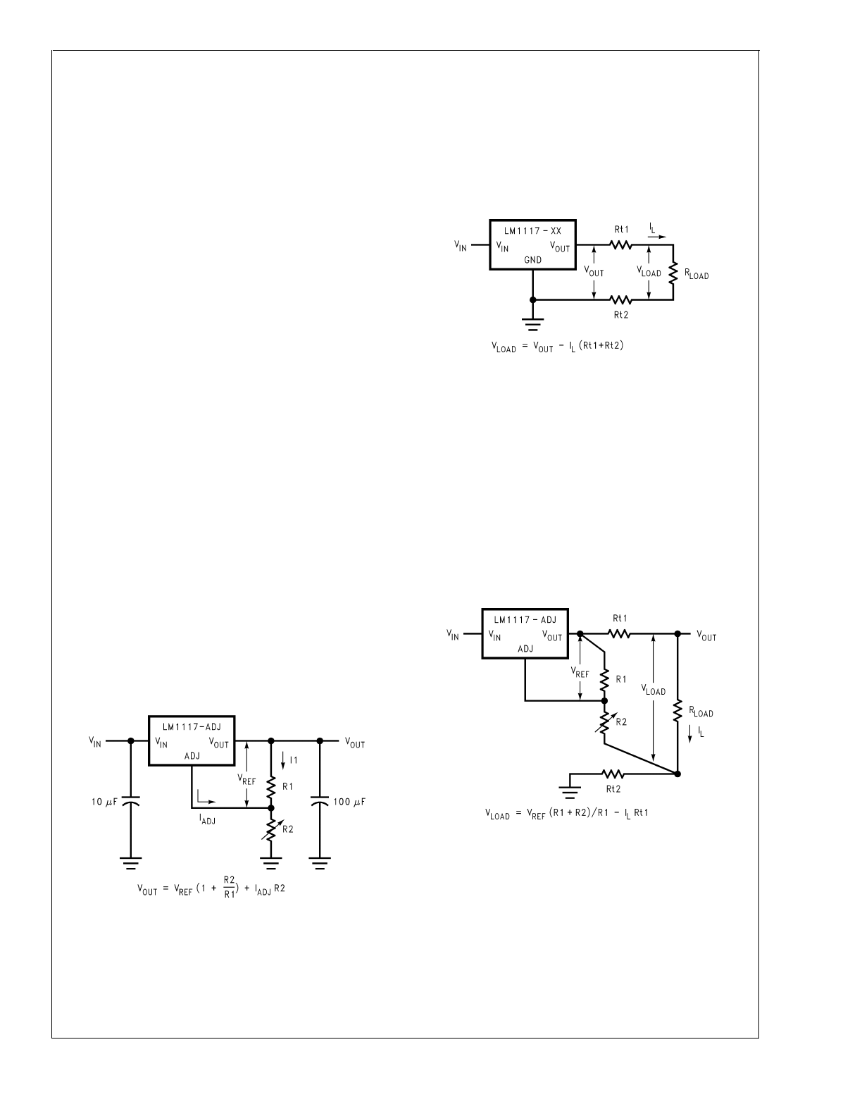
3.0 Load Regulation
The LM1117 regulates the voltage that appears between its
output and ground pins, or between its output and adjust
pins. In some cases, line resistances can introduce errors to
the voltage across the load. To obtain the best load regula-
tion, a few precautions are needed.
Figure 2
, shows a typical application using a fixed output
regulator. The Rt1 and Rt2 are the line resistances. It is
obvious that the V
LOAD
is less than the V
OUT
by the sum of
the voltage drops along the line resistances. In this case, the
load regulation seen at the R
LOAD
would be degraded from
the data sheet specification. To improve this, the load should
be tied directly to the output terminal on the positive side and
directly tied to the ground terminal on the negative side.
When the adjustable regulator is used (
Figure 3
), the best
performance is obtained with the positive side of the resistor
R1 tied directly to the output terminal of the regulator rather
than near the load. This eliminates line drops from appearing
effectively in series with the reference and degrading regu-
lation. For example, a 5V regulator with 0.05
Ω
resistance
between the regulator and load will have a load regulation
due to line resistance of 0.05
Ω
x I
L
. If R1 (=125
Ω
) is con-
nected near the load, the effective line resistance will be
0.05
Ω
(1+R2/R1) or in this case, it is 4 times worse. In
addition, the ground side of the resistor R2 can be returned
near the ground of the load to provide remote ground sens-
ing and improve load regulation.
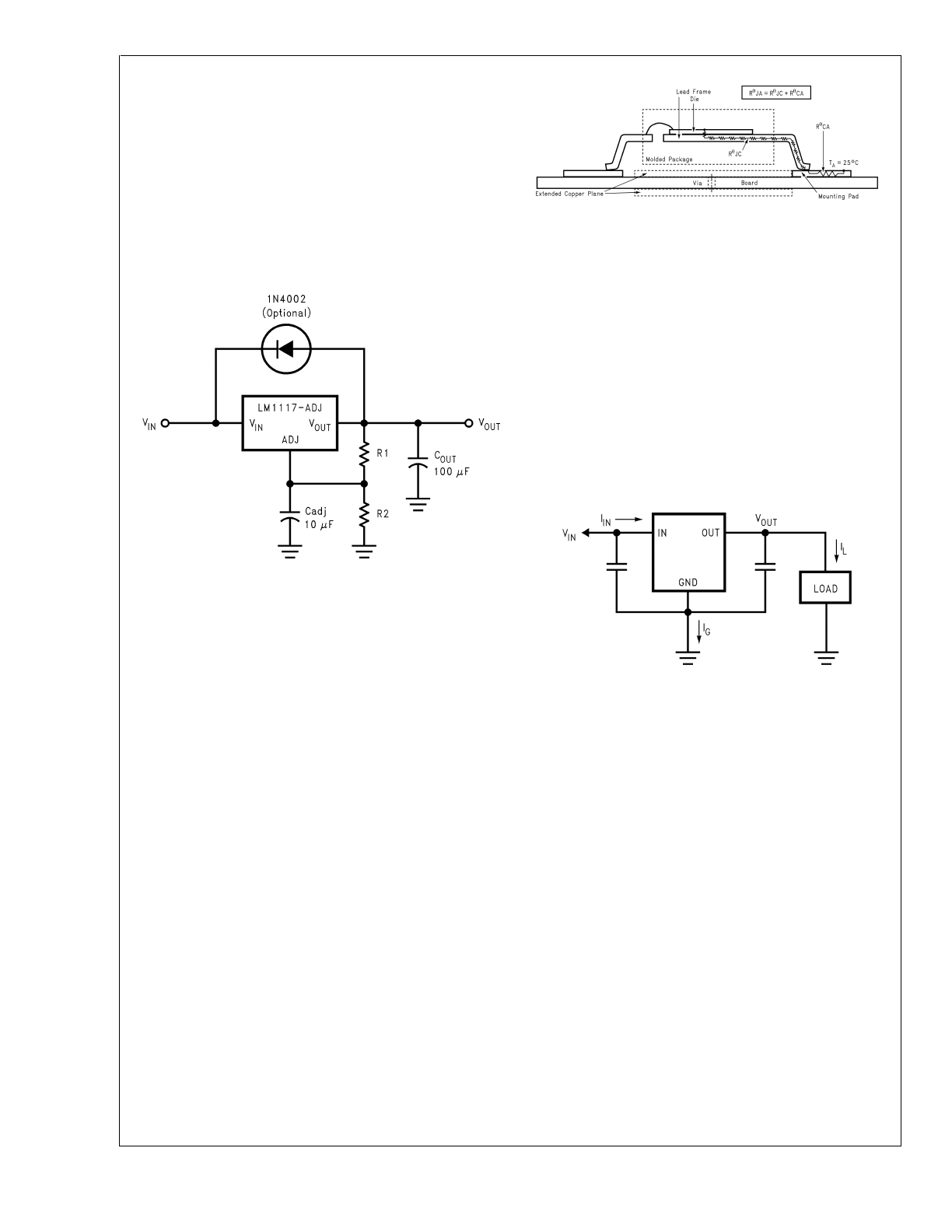
4.0 Protection Diodes
Under normal operation, the LM1117 regulators do not need
any protection diode. With the adjustable device, the internal
resistance between the adjust and output terminals limits the
current. No diode is needed to divert the current around the
regulator even with capacitor on the adjust terminal. The
adjust pin can take a transient signal of
±
25V with respect to
the output voltage without damaging the device.
When a output capacitor is connected to a regulator and the
input is shorted to ground, the output capacitor will discharge
DS100919-17
FIGURE 1. Basic Adjustable Regulator
DS100919-18
FIGURE 2. Typical Application using Fixed Output
Regulator
DS100919-19
FIGURE 3. Best Load Regulation using Adjustable
Output Regulator
LM1
1
17/LM1
1
17I
www.national.com
9
APPLICATION NOTE
(Continued)
into the output of the regulator. The discharge current de-
pends on the value of the capacitor, the output voltage of the
regulator, and rate of decrease of V
IN
. In the LM1117 regu-
lators, the internal diode between the output and input pins
can withstand microsecond surge currents of 10A to 20A.
With an extremely large output capacitor (
≥
1000 µF), and
with input instantaneously shorted to ground, the regulator
could be damaged.
In this case, an external diode is recommended between the
output and input pins to protect the regulator, as shown in
Figure 4
.
5.0 Heatsink Requirements
When an integrated circuit operates with an appreciable
current, its junction temperature is elevated. It is important to
quantify its thermal limits in order to achieve acceptable
performance and reliability. This limit is determined by sum-
ming the individual parts consisting of a series of tempera-
ture rises from the semiconductor junction to the operating
environment. A one-dimensional steady-state model of con-
duction heat transfer is demonstrated in
Figure 5
. The heat
generated at the device junction flows through the die to the
die attach pad, through the lead frame to the surrounding
case material, to the printed circuit board, and eventually to
the ambient environment. Below is a list of variables that
may affect the thermal resistance and in turn the need for a
heatsink.
R
θ
JC
(Component Vari-
ables)
R
θ
CA
(Application Vari-
ables)
Leadframe Size &
Material
Mounting Pad Size,
Material, & Location
No. of Conduction Pins
Placement of Mounting
Pad
Die Size
PCB Size & Material
Die Attach Material
Traces Length & Width
Molding Compound Size
and Material
Adjacent Heat Sources
Volume of Air
Ambient Temperatue
Shape of Mounting Pad
The LM1117 regulators have internal thermal shutdown to
protect the device from over-heating. Under all possible
operating conditions, the junction temperature of the LM1117
must be within the range of 0˚C to 125˚C. A heatsink may be
required depending on the maximum power dissipation and
maximum ambient temperature of the application. To deter-
mine if a heatsink is needed, the power dissipated by the
regulator, P
D
, must be calculated:
I
IN
= I
L
+ I
G
P
D
= (V
IN
-V
OUT
)I
L
+ V
IN
I
G
Figure 6
shows the voltages and currents which are present
in the circuit.
DS100919-15
FIGURE 4. Regulator with Protection Diode
DS100919-37
FIGURE 5. Cross-sectional view of Integrated Circuit
Mounted on a printed circuit board. Note that the case
temperature is measured at the point where the leads
contact with the mounting pad surface
DS100919-16
FIGURE 6. Power Dissipation Diagram
LM1
1
17/LM1
1
17I
www.national.com
10
APPLICATION NOTE
(Continued)
The next parameter which must be calculated is the maxi-
mum allowable temperature rise, T
R
(max):
T
R
(max) = T
J
(max)-T
A
(max)
where T
J
(max) is the maximum allowable junction tempera-
ture (125˚C), and T
A
(max) is the maximum ambient tem-
perature which will be encountered in the application.
Using the calculated values for T
R
(max) and P
D
, the maxi-
mum allowable value for the junction-to-ambient thermal
resistance (
θ
JA
) can be calculated:
θ
JA
= T
R
(max)/P
D
If the maximum allowable value for
θ
JA
is found to be
≥
136˚C/W for SOT-223 package or
≥
79˚C/W for TO-220
package or
≥
92˚C/W for TO-252 package, no heatsink is
needed since the package alone will dissipate enough heat
to satisfy these requirements. If the calculated value for
θ
JA
falls below these limits, a heatsink is required.
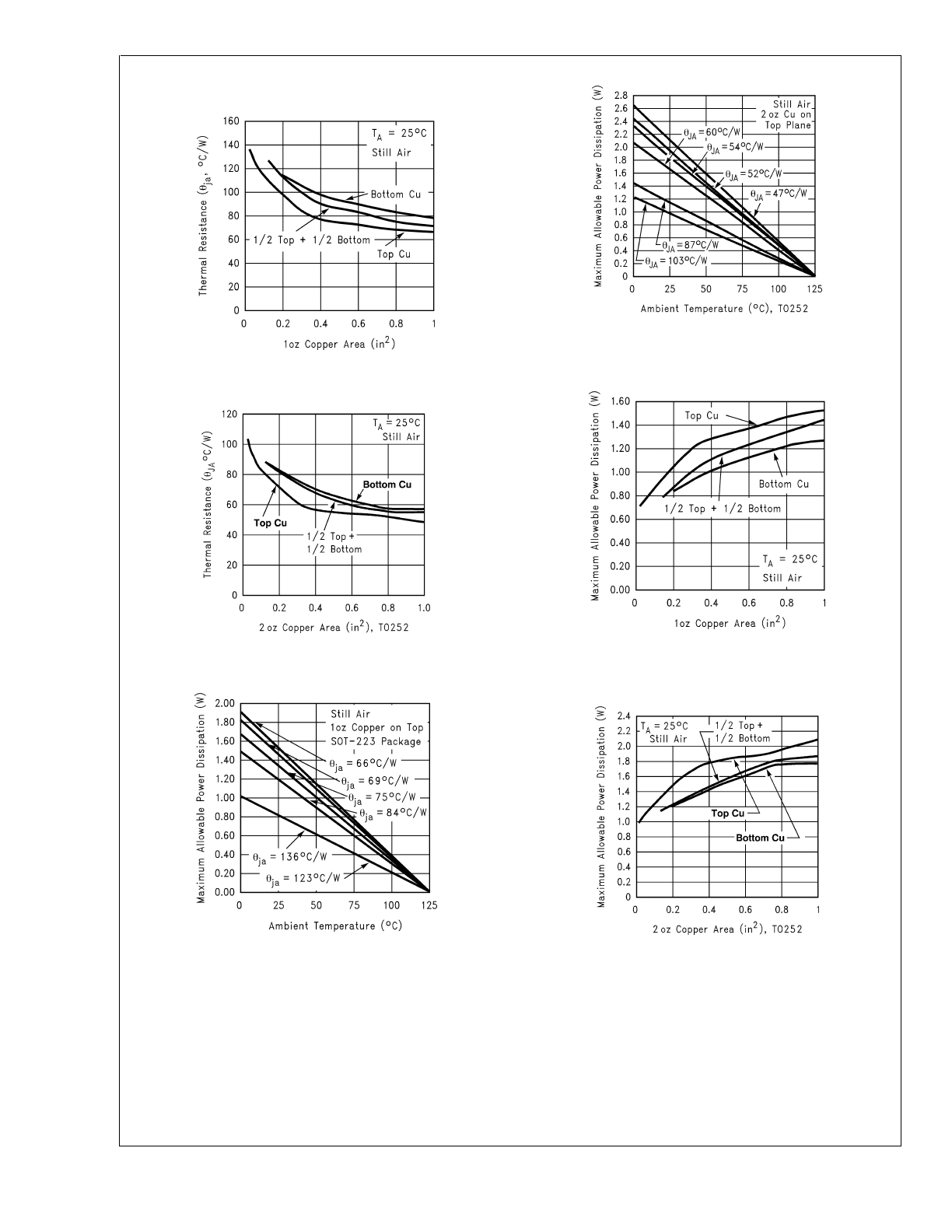
As a design aid,
Table 1
shows the value of the
θ
JA
of
SOT-223 and TO-252 for different heatsink area. The copper
patterns that we used to measure these
θ
JA
s are shown at
the end of the Application Notes Section.
Figure 7
and
Figure
8
reflects the same test results as what are in the
Table 1
Figure 9
and
Figure 10
shows the maximum allowable power
dissipation vs. ambient temperature for the SOT-223 and
TO-252 device. Figures
Figure 11
and
Figure 12
shows the
maximum allowable power dissipation vs. copper area (in
2
)
for the SOT-223 and TO-252 devices. Please see AN1028
for power enhancement techniques to be used with SOT-223
and TO-252 packages.
TABLE 1.
θ
JA
Different Heatsink Area
Layout
Copper Area
Thermal Resistance
Top Side (in
2
)*
Bottom Side (in
2
)
(
θ
JA
,˚C/W) SOT-223
(
θ
JA
,˚C/W) TO-252
1
0.0123
0
136
103
2
0.066
0
123
87
3
0.3
0
84
60
4
0.53
0
75
54
5
0.76
0
69
52
6
1
0
66
47
7
0
0.2
115
84
8
0
0.4
98
70
9
0
0.6
89
63
10
0
0.8
82
57
11
0
1
79
57
12
0.066
0.066
125
89
13
0.175
0.175
93
72
14
0.284
0.284
83
61
15
0.392
0.392
75
55
16
0.5
0.5
70
53
*Tab of device attached to topside copper
LM1
1
17/LM1
1
17I
www.national.com
11
APPLICATION NOTE
(Continued)
DS100919-13
FIGURE 7.
θ
JA
vs. 1oz Copper Area for SOT-223
DS100919-34
FIGURE 8.
θ
JA
vs. 2oz Copper Area for TO-252
DS100919-12
FIGURE 9. Maximum Allowable Power Dissipation vs.
Ambient Temperature for SOT-223
DS100919-36
FIGURE 10. Maximum Allowable Power Dissipation vs.
Ambient Temperature for TO-252
DS100919-14
FIGURE 11. Maximum Allowable Power Dissipation vs.
1oz Copper Area for SOT-223
DS100919-35
FIGURE 12. Maximum Allowable Power Dissipation vs.
2oz Copper Area for TO-252
LM1
1
17/LM1
1
17I
www.national.com
12
APPLICATION NOTE
(Continued)
DS100919-41
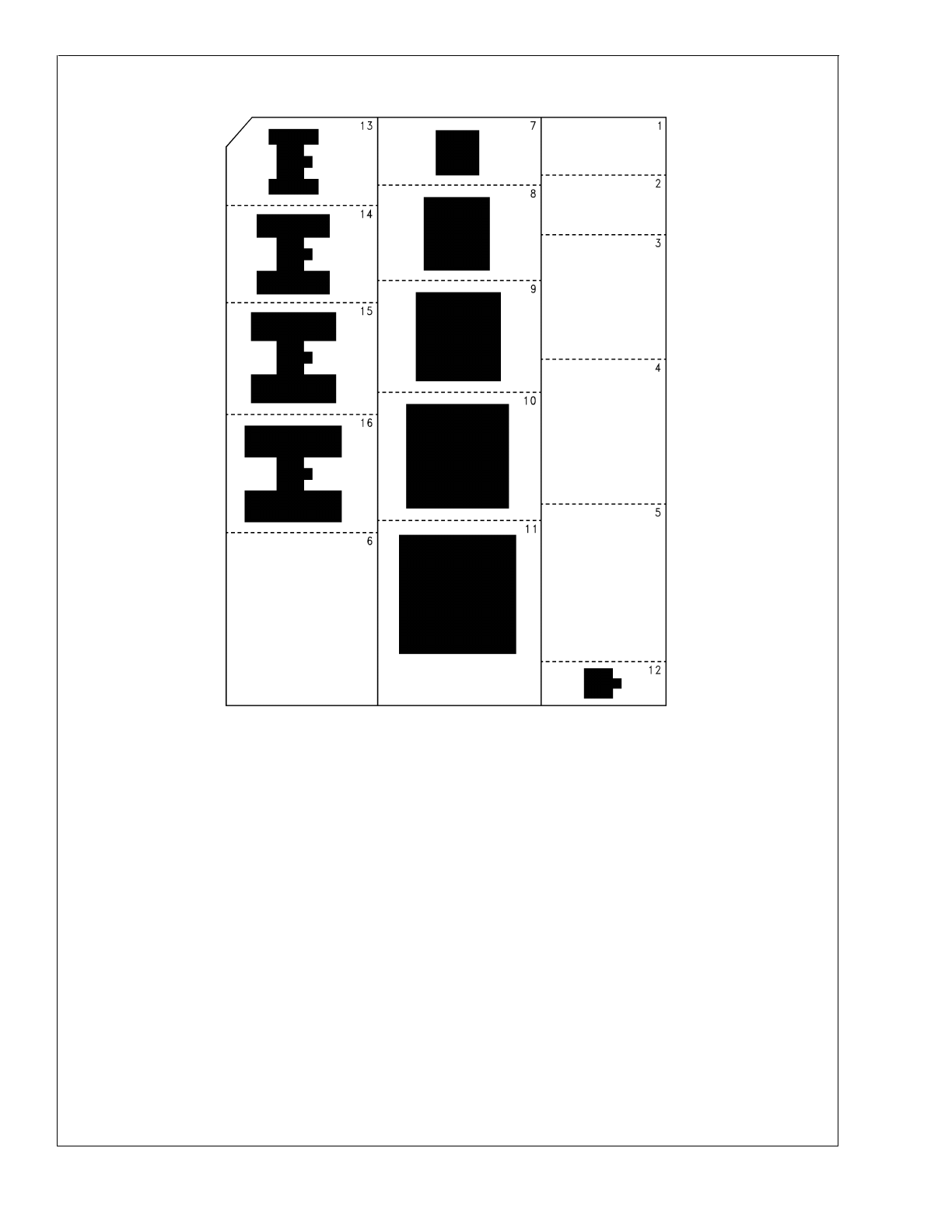
FIGURE 13. Top View of the Thermal Test Pattern in Actual Scale
LM1
1
17/LM1
1
17I
www.national.com
13
APPLICATION NOTE
(Continued)
DS100919-42
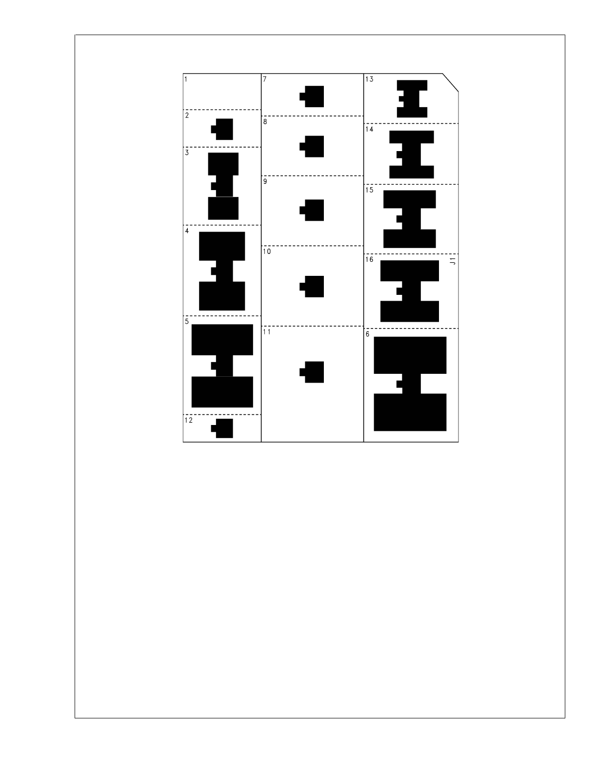
FIGURE 14. Bottom View of the Thermal Test Pattern in Actual Scale
LM1
1
17/LM1
1
17I
www.national.com
14
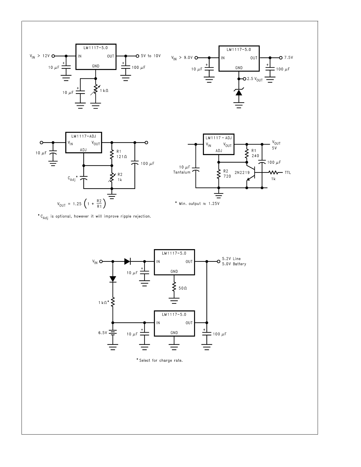
Typical Application Circuits
DS100919-30
Adjusting Output of Fixed Regulators
DS100919-31
Regulator with Reference
DS100919-29
1.25V to 10V Adjustable Regulator with Improved
Ripple Rejection
DS100919-27
5V Logic Regulator with Electronic Shutdown*
DS100919-32
Battery Backed-Up Regulated Supply
LM1
1
17/LM1
1
17I
www.national.com
15
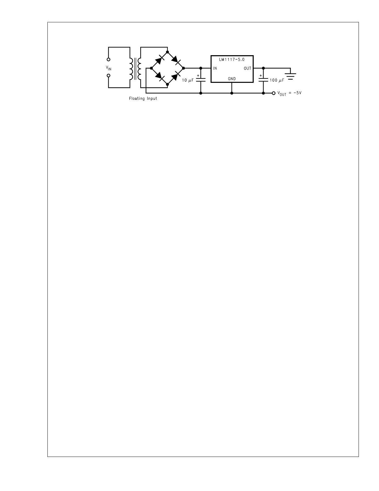
Typical Application Circuits
(Continued)
DS100919-33
Low Dropout Negative Supply
LM1
1
17/LM1
1
17I
www.national.com
16
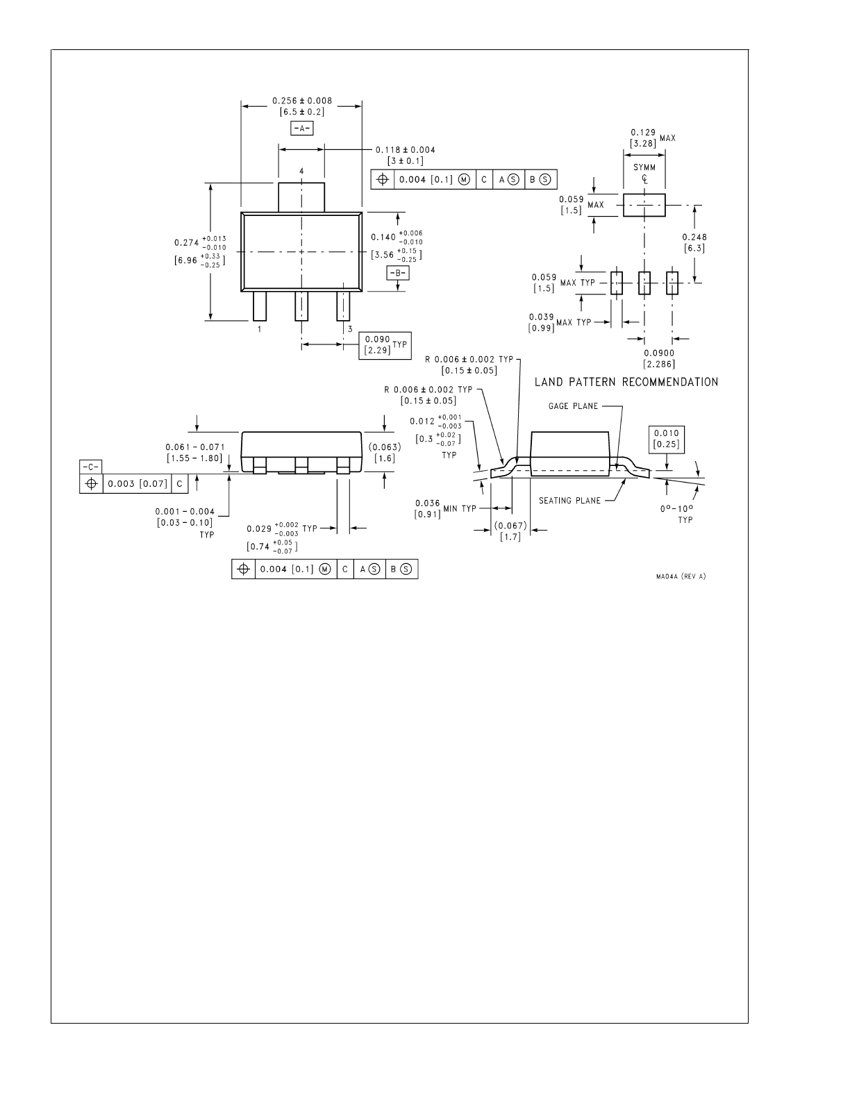
Physical Dimensions
inches (millimeters) unless otherwise noted
3-Lead SOT-223
NS Package Number MA04A
LM1
1
17/LM1
1
17I
www.national.com
17
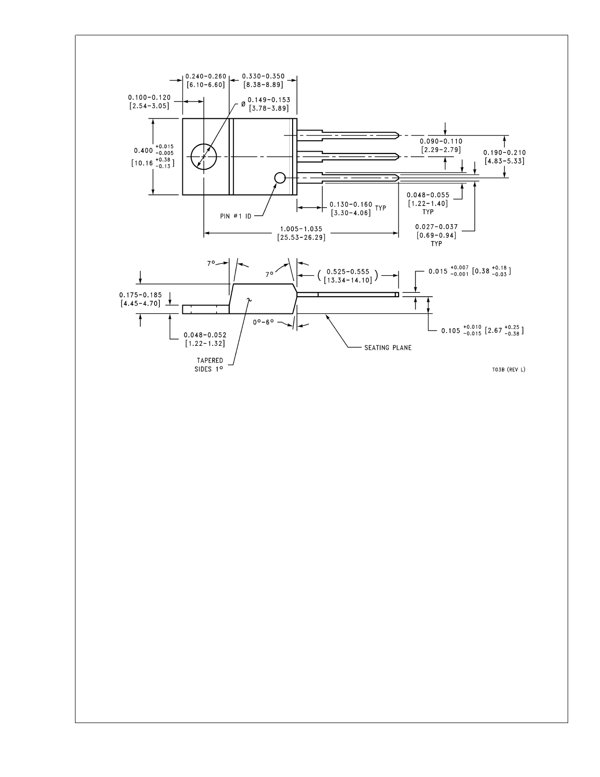
Physical Dimensions
inches (millimeters) unless otherwise noted (Continued)
3-Lead TO-220
NS Package Number T03B
LM1
1
17/LM1
1
17I
www.national.com
18
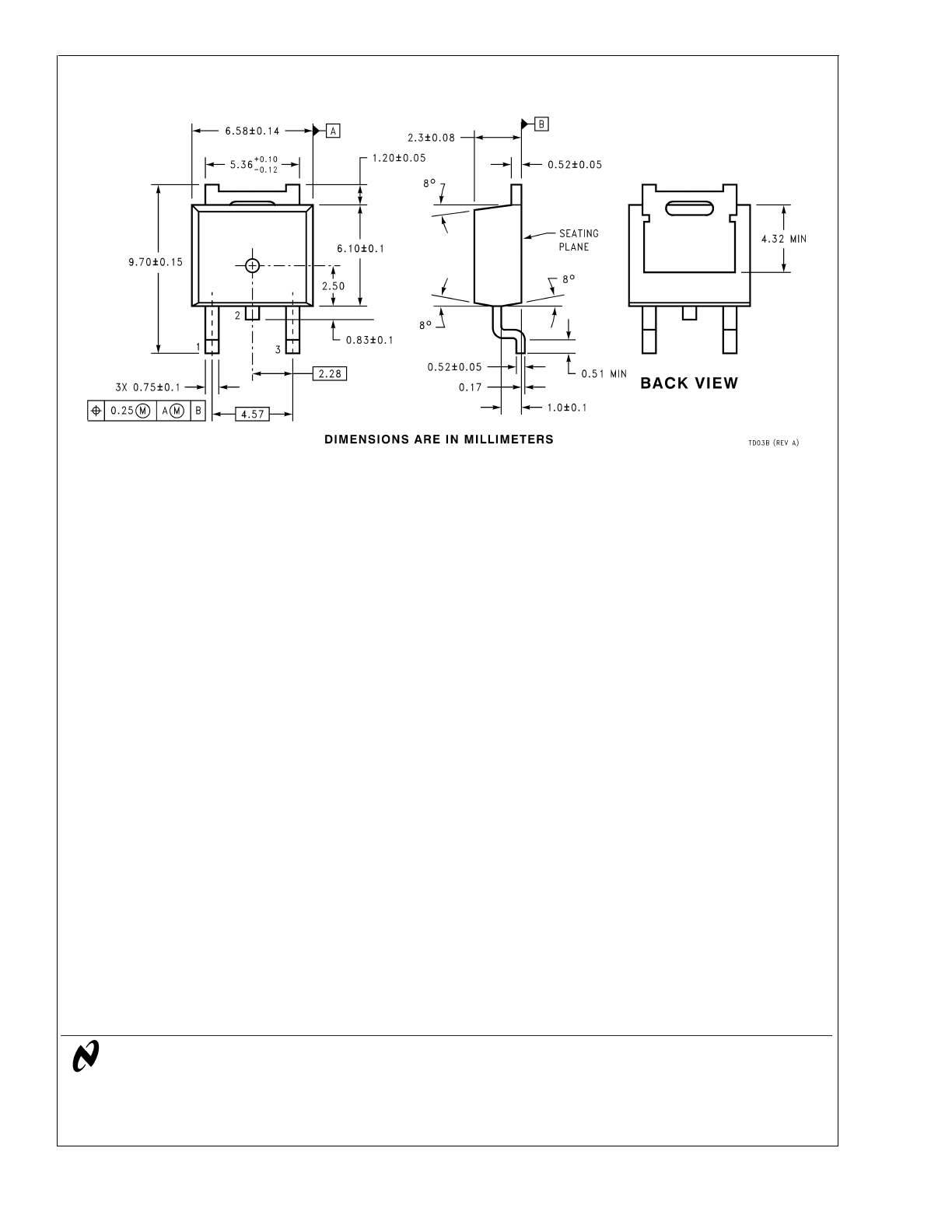
Physical Dimensions
inches (millimeters) unless otherwise noted (Continued)
LIFE SUPPORT POLICY
NATIONAL’S PRODUCTS ARE NOT AUTHORIZED FOR USE AS CRITICAL COMPONENTS IN LIFE SUPPORT
DEVICES OR SYSTEMS WITHOUT THE EXPRESS WRITTEN APPROVAL OF THE PRESIDENT AND GENERAL
COUNSEL OF NATIONAL SEMICONDUCTOR CORPORATION. As used herein:
1. Life support devices or systems are devices or
systems which, (a) are intended for surgical implant
into the body, or (b) support or sustain life, and
whose failure to perform when properly used in
accordance with instructions for use provided in the
labeling, can be reasonably expected to result in a
significant injury to the user.
2. A critical component is any component of a life
support device or system whose failure to perform
can be reasonably expected to cause the failure of
the life support device or system, or to affect its
safety or effectiveness.
National Semiconductor
Corporation
Americas
Email: support@nsc.com
National Semiconductor
Europe
Fax: +49 (0) 180-530 85 86
Email: europe.support@nsc.com
Deutsch Tel: +49 (0) 69 9508 6208
English
Tel: +44 (0) 870 24 0 2171
Français Tel: +33 (0) 1 41 91 8790
National Semiconductor
Asia Pacific Customer
Response Group
Tel: 65-2544466
Fax: 65-2504466
Email: ap.support@nsc.com
National Semiconductor
Japan Ltd.
Tel: 81-3-5639-7560
Fax: 81-3-5639-7507
www.national.com
3-Lead TO-252
NS Package Number TD03B
LM1
1
17/LM1
1
17I
800mA
Low-Dropout
Linear
Regulator
National does not assume any responsibility for use of any circuitry described, no circuit patent licenses are implied and National reserves the right at any time without notice to change said circuitry and specifications.